SEMICON Taiwan 2026 CPO 全记录:激光器是最紧的约束,测试产能决定时间表 —— Jason's Chips 会议综述精读
一场会议把「光学要不要进封装」的争论结束,换成了三个更硬的问题:激光器够不够多、封装良率稳不稳、测试产能跟不跟得上。附 14 家厂商的完整陈述、22 张现场幻灯片与英文原文全文。
来源:Jason’s Chips(@jasonschips)的 X 长文,发布于 2026 年 9 月下旬。作者为该专栏独立投资人,文风为个人投资者视角。 原文:SEMICON Taiwan—CPO — https://x.com/jasonschips/article/2104261655106367611 会议:SEMICON Taiwan 2026(论坛自 2026 年 8 月 31 日起,主展 9 月 2–4 日,台北南港展览馆)。原文覆盖 Marvell、Lightmatter、TSMC、UMC、imec、Soitec、Lumentum、Coherent、SMART Photonics、ASE、Lam Research、Onto Innovation、ficonTEC、Advantest 共 14 家。 转载说明:第一部分为英文原文完整转载,含全部 22 张会议现场幻灯片配图(图注为本站所加中文说明),版权归原作者所有;本站仅调整排版与标题层级、不改动任何文字表述。第二部分为本站独立撰写的中文结构化解读,其中的质疑、推算与判断属解读者观点,不构成投资建议。
第一部分:英文原文(Original Article)
SEMICON Taiwan is the semiconductor industry’s big annual trade show in Taipei, and next to the exhibition floor it runs a set of technical forums where the supply chain presents. Unlike Hot Chips, SEMICON is generally very manufacturing rather than design-focused. Which to be honest is more useful to your everyday bottleneck bro investor. This post is about the presentations related to optics!
A 101 before we dive down the rabbit hole. An optical link has 4 parts. A laser makes a steady beam of light, and a modulator switches that beam on and off, or between levels, to write bits onto it. A fiber carries the light to a photodetector at the far end, which turns it back into electrical current. A transceiver is those parts in a box, and a pluggable transceiver is the version that plugs into the faceplate of a switch. A link’s bandwidth is split across lanes, parallel streams of bits, so speeds are quoted per lane (200G per lane). Copper does the same job with no conversion at all, and it is cheaper, so optics only wins where copper cannot reach at the required data rate.
Optics is moving deeper into the AI server in stages, and the stages are stages of co-packaged optics (CPO), where the optics move out of a pluggable module and into the package next to the chip. Stage 0 is the pluggable transceiver for scale-out, the network that links racks and pods (groups of racks), which has been optical for years. Stage 1 is CPO for those same scale-out links, which moves the optics from the switch faceplate into the switch package to cut power. Stage 2 is CPO for scale-up between racks. Scale-up is the network between GPUs that share memory as 1 machine, and optics between racks lets that domain grow past the GPUs that fit in 1 copper rack. Stage 3 is CPO for scale-up inside the rack, which replaces copper once the bandwidth per lane is too high for copper to carry.
Stage 4 is optical I/O (or scale-in) where the optical engine moves onto the interposer next to the GPU itself. The optical engine is the laser, modulator and detector assembly that replaces a transceiver, and the interposer is the slice of silicon the GPU and its high-bandwidth memory (HBM) stacks already sit on. From the interposer, the engine can carry GPU-to-HBM traffic, so memory can be disaggregated from the GPU.
Stage 0 is done and stage 1 is shipping. Most of the conference argued about stages 2 and 3, and the forward-looking talks ended up in stage 4.
These talks are organized into a bunch of categories. I start with the network case, because it explains why anyone is building any of this. Then I take the foundry platforms and the argument about which material modulates the light past 200G per lane, then the lasers, then the packagers and tool vendors, and finally the test vendors, who think the industry’s CPO timelines are too fast.
- Networks
- Foundries
- Lasers
- Manufacturing
- Test
- Conference Takeaways
Networks
To understand why scale-up optics is needed, you need to understand where networking requirements are headed.
Marvell Connectivity
Marvell sells the digital signal processors (DSPs), switch silicon and silicon photonics engines that sit between the chips and the fiber, at every distance from inside the package to between data centers. Its market grows with cluster size. GPT-5 was trained on 50K-100K accelerators, and today’s models train on 1m-accelerator clusters, which need 10m optical interconnects. In addition, relative to the bandwidth of the end user connecting over the wide-area network, a traditional data center’s front-end network, the one facing users and storage, generates 7x the traffic. By contrast, an AI data center generates 14x at the front end, 56x in the scale-out network and 500x in the scale-up network, and the 500x tier is the one still on copper.
Pluggable optics have hit an energy ceiling. A 1.6T pluggable transceiver burns 10 picojoules per bit, and the number has stopped falling, because the DSP inside the pluggable that cleans up the signal scales with the data rate. By contrast, CPO gets to 2-5 pJ/bit. Putting the optics next to the switch chip deletes the electrical SerDes, the circuits that drove the pluggable’s signal across the board, and that is where the 5-6x energy improvement every CPO vendor quotes comes from.
Each distance tier runs its own modulation. Inside the server and rack the signaling is NRZ, 1 bit per symbol, over 10 m or less. Scale-out pluggables up to 1.6T run PAM4, where 4 signal levels carry 2 bits per symbol. Scale-across, the links between data centers, runs coherent 16-QAM (vs IMDD for both scale-up and scale-out) over hundreds of kilometers, where 16 combinations of phase and brightness carry 4 bits per symbol. However, every extra level per symbol costs signal-to-noise margin, and optics has less margin to spend than copper. At 400G per lane, copper can therefore move to PAM6 while optics stays at PAM4.
Past 400G, Marvell is pursuing every modulator at once. For long reach it has thin-film lithium niobate (TFLN) and micro-ring modulators. A micro-ring is a tiny loop of waveguide, the on-chip channel that carries light, and each ring is tuned to 1 wavelength. For scale-up fabrics Marvell has electro-absorption modulators, micro-LEDs, micro-VCSELs and plasmonics. However, in optics the fastest modulators are also the largest. A TFLN Mach-Zehnder modulator, which splits the beam down 2 arms and recombines it, takes 100x the area of a micro-VCSEL, and nothing is both small and fast yet.
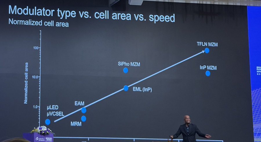
图 1|Marvell:调制器类型 vs 单元面积 vs 速度。归一化单元面积(纵轴,对数)与调制速度(横轴)几乎成正比——TFLN MZM 面积最大也最快,µLED / µVCSEL 最小最慢,目前还没有既小又快的器件。
Plasmonics is Marvell’s candidate for a modulator that is both. The plasmonic modulator is a 10-20 micron metallic waveguide with an electro-optic polymer in the middle, and it carries the signal in the electron waves at the metal surface rather than in the glass. It has been measured at 990 GHz of bandwidth, against 110 GHz for today’s best conventional modulators, which makes it Marvell’s path to 800G per lane. Nothing else on the roadmap reaches 800G today. When asked for a timeline, the Marvell speaker said to ask him again in 5 years.
The CPO hardware Marvell ships today is a 2.5D engine. A driver and a transimpedance amplifier (which turns the photodetector’s current into a voltage) sit on a silicon photonics interposer with through-silicon vias, and the assembly is built chip-on-wafer and then wafer-on-substrate. The engine runs 32 lanes at 224G, and the fiber joins the die at its edge. The second generation is in production, and Marvell is moving development from the third generation to the fourth.
CPO also inverts the switch faceplate. The external laser modules (ELSFPs, the pluggable-shaped modules that feed light into the package) take up most of it, and the whole chassis is water cooled. When asked whether CPO designs still need spare engines for redundancy, the Marvell speaker said silicon photonics handles it at the system level, by rerouting around a failed engine. By contrast, micro-LED designs handle it in hardware, by switching to a spare emitter, because they have far more emitters to spare.
Lightmatter Passage and Guide
Lightmatter is a photonic interconnect startup with design-ins at NVIDIA and Qualcomm. It sells Passage, an optical engine, and Guide, a laser chip that feeds Passage. Lightmatter’s talk was based because they argued for why a big scale-up domain is important in the first place. Sometimes knowing what questions to ask is more important than having the answer to it!
Lightmatter has 2 peer-reviewed results. The training result compares 4 pods of 144 GPUs, linked to each other at scale-out bandwidth, against a single 512-GPU scale-up domain at the same power. That baseline is conservative, because 1 rack of 72 against a 576-GPU domain would be a more dramatic contrast. At the same 14.4 Tb/s of scale-up bandwidth per GPU, the 512-GPU domain trains a trillion-parameter mixture-of-experts model in 0.60x the time. At 32 Tb/s per GPU, which Lightmatter considers an easy number, the time drops to 0.37x, close to 3x faster.
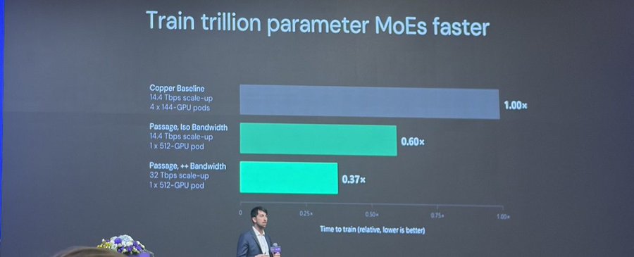
图 2|Lightmatter:训练万亿参数 MoE 的相对耗时。以 4×144-GPU 铜互连 pod(1.00x)为基准,512-GPU 光 scale-up 域在同等 14.4 Tb/s 带宽下是 0.60x,带宽提到 32 Tb/s 后降到 0.37x。
The inference result is the same experiment applied to the 2 phases of serving a model. Prefill is the phase where the model reads the whole prompt, and time to first token at a 131K-token context falls by 3x. Decode is the phase where the model generates tokens 1 at a time, and tokens per second per user doubles.
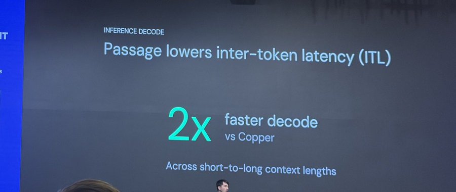
图 3|Lightmatter:推理 Decode 阶段的 inter-token latency(ITL)相比铜降低 2 倍,且该收益在短到长上下文区间都成立。
These numbers come from domain size rather than from Lightmatter’s engine. A model that is split across many GPUs has to move activations between them at every layer, and in a mixture-of-experts model every token is also routed to expert blocks on other GPUs. Inside 1 copper domain those transfers run at full scale-up bandwidth. However, once a job spans several pods, the transfers that cross a pod boundary drop to scale-out bandwidth, and the GPUs wait.
In training, the waiting shows up as low utilization of the GPU’s math units, so the same GPUs take longer to finish the same number of steps. In prefill, a 131K-token prompt is a large parallel computation, so it can be split across more GPUs when they all sit in 1 domain, and each request finishes sooner. In decode, each generated token requires re-reading the model’s weights. Spreading the model across more GPUs in 1 domain means each GPU reads a smaller slice of the weights per step, so each step is faster, and that is the doubling of tokens per second per user. Alternatively, the same headroom can go to batching more users at the old speed, which raises total tokens served. A larger scale-up domain therefore improves the whole trade-off between speed per user and total tokens served, and copper caps the domain at 1 rack.
Lightmatter’s CEO said the industry’s goal is a 1,000-GPU domain that programs like 1 GPU, which is 16 racks of 64 GPUs where the programmer never has to partition the workload between racks.
Lightmatter’s CEO said photonics has been treated as a dongle for electrical SerDes (lol), so its speeds followed the SerDes roadmap of 56G, 112G and 224G. Around OFC (the optical industry’s main conference) in March 2026, OpenAI, Broadcom, AMD, NVIDIA and others announced the OCI MSA, a multi-source agreement that defines the scale-up optical link, and he said it is the first standard written for the optics rather than for the SerDes. OCI allows you to go slow-and-wide right from the chip rather than having to serialize. The OCI link carries many colors of light in 1 fiber, which is dense wavelength-division multiplexing (DWDM), and it sends and receives on the same fiber, which makes it bidirectional. Micro-ring modulators are its default modulator. Lightmatter shipped DWDM bidirectional links in 2024 at 800G per fiber, and it showed 1,600G per fiber at OFC 2026.
On a 512-GPU cluster, putting transmit and receive on 1 fiber instead of 2 removes 240 km of fiber and 20,000 optical connectors, and at gigawatt scale it takes 16% off the total networking bill. Scale-up networking is going to 10x the industry’s fiber consumption, so Lightmatter’s CEO expects operators to prefer the bidirectional design.
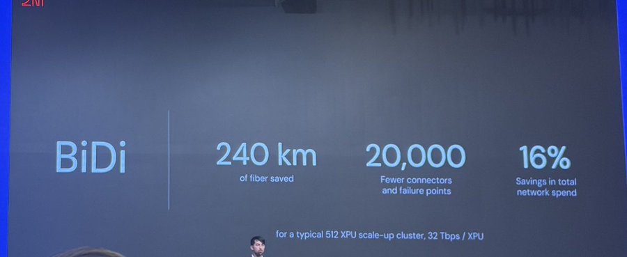
图 4|Lightmatter:BiDi(单纤双向)的收益。对一个典型 512 XPU、32 Tb/s/XPI 的 scale-up 集群,可省下 240 km 光纤、减少 20,000 个连接器与故障点,总网络开销降低 16%。
The first form of stage 2 to ship is near-package optics (NPO), where the optical engine sits on the board next to the chip rather than inside its package. Lightmatter’s Passage L20 is a 224G NPO engine at 30 W, which is 4.8 pJ/bit. Since NVIDIA’s Computex announcement in May 2026, it has been part of the NVLink ecosystem, in 3 form factors: chip-on-board, a mezzanine card called CPX, and the XPO standard Lightmatter co-founded with Arista. Lightmatter’s CEO puts NPO in 2027, CPO at the end of 2028 and optical I/O on the interposer around the same time.
NPO comes first because CPO’s supply chain and test are not ready, and test is a volume problem. Each GPU carries 4-8 optical engines, and scale-out is 10% of the engine volume of scale-up. Scale-up therefore needs 10-100x the optical engine testing the industry does today. In addition, the die has to yield, because it is attached to a $50K GPU.
Every optical link needs laser power in proportion to its bandwidth. Today it takes 16-18 ELSFPs to power a 100T switch, and 128 for an 800T switch. The laser makers have pushed a discrete indium phosphide laser to 400 mW, which is close to the power at which the fiber itself is damaged, so power per laser cannot keep rising. Doubling bandwidth therefore means doubling the laser count, and laser cost and area double with it.
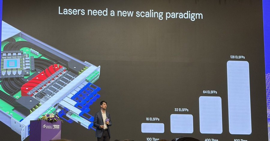
图 5|Lightmatter:激光器需要新的扩展范式。100 Tb/s / 400 Tb/s / 800 Tb/s 交换机分别需要 16 / 64 / 128 个 ELSFP 模块——激光功率封顶后,带宽翻倍就意味着激光器数量翻倍。
Lightmatter’s answer is Guide. Guide 1 puts 128 lasers on a single chip, with room to grow to 500-1,000, and it is built in a 300 mm CMOS foundry because Lightmatter’s CEO thinks 10% a year of foundry progress compounds faster than any new material can catch up. He said you do not bet against silicon. An on-chip ASIC monitors the array and routes in a spare laser when one fails, so the failure rate is 0.1 FIT (0.1 failures per 1b device-hours).
A micro-ring modulator has to lock onto its laser line, and a conventional laser array drifts in both power and frequency, so the rings spend constant effort tracking it. By contrast, Guide 1 holds power to within 0.25 dB and frequency to within 3 GHz.
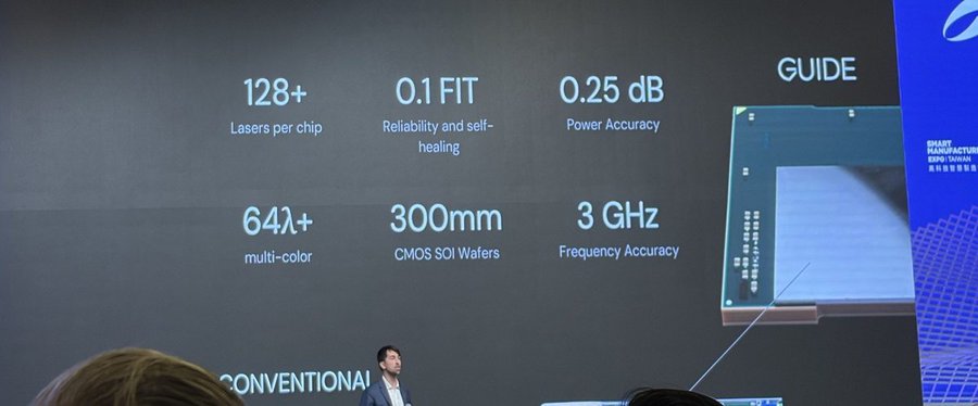
图 6|Lightmatter Guide 激光芯片指标:单芯片 128+ 激光器(可扩展到 500–1,000)、0.1 FIT 的可靠性与自愈、0.25 dB 功率精度、64λ+ 多色、300 mm CMOS SOI 晶圆、3 GHz 频率精度。
Hyperscalers and chip companies are sampling Guide 1 at 16 colors today, and the design can carry 64.
Foundries
The foundries decide what an optical engine can be built from. Normally that’s SOI, but above 200G per lane it becomes an open question, because silicon modulators run out of speed.
TSMC COUPE
I think TSMC’s talk was the most important of the foundry talks, because it was the first time I have seen a presenter formally separate CPO from optical I/O (or scale-up and scale-in) as 2 different products.
The links into and out of a chip scale slower than anything else in the system, which TSMC calls the I/O wall. AI compute grows 3x every 2 years, memory bandwidth 1.6x, and interconnect bandwidth only 1.4x.
TSMC splits what the industry calls CPO into 2 products. CPO-MCM puts the optical engine on the package substrate next to a switch chip, in a multi-chip module, and CPO has meant this until now. CPO-OOI, for optics on interposer, puts the optical engine directly on the interposer of the XPU (the accelerator die, GPU or otherwise). There the engine is 1 hop from the XPU and its HBM, so it can carry the XPU’s memory traffic, which is the stage 4 case.
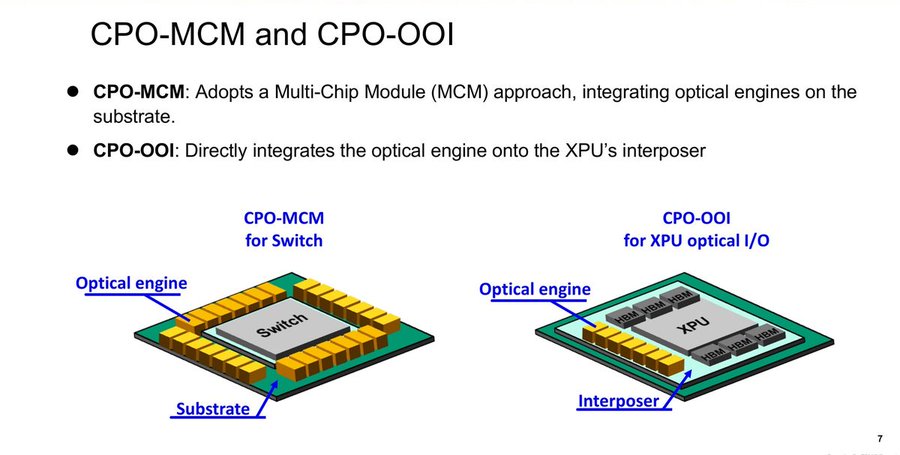
图 7|TSMC:CPO-MCM 与 CPO-OOI 的区分。CPO-MCM 把光引擎放在多芯片模块(MCM)的基板上,配套交换芯片;CPO-OOI 把光引擎直接放到 XPU 的中介层上。
Relative to copper, pluggable optics are 2x more energy efficient at the same latency, CPO is 4x more efficient at under 0.1x the latency, and optics on interposer is 10x more efficient at under 0.05x the latency.
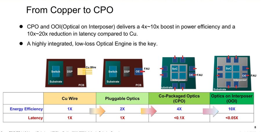
图 8|TSMC:从铜到 CPO。功耗效率依次为 1x(铜线)/ 2x(可插拔光模块)/ 4x(CPO)/ 10x(中介层光学 OOI);延迟分别为 1x / 1x / <0.1x / <0.05x。
COUPE stands for compact universal photonic engine. It is an electronic die bonded face to face onto a photonic die with TSMC’s SoIC hybrid bond. The stack is built chip-on-wafer first, then wafer-on-wafer onto a silicon carrier, and light reaches the photonic die through a silicon micro-lens and a copper reflector on the back side. COUPE comes in 2 versions. In the grating-coupled version the fiber’s light drops in from above through a grating, and in the edge-coupled version it enters from the side of the die through a silicon nitride tip. TSMC’s process design kit (PDK), the library of verified parts a customer designs a chip from, already carries the building blocks, from silicon and silicon nitride waveguides to micro-ring modulators, germanium photodetectors and thermal phase shifters.
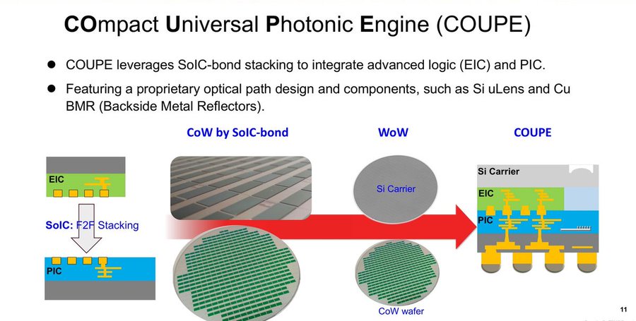
图 9|TSMC:COUPE 结构。电子裸片(EIC)与光子裸片(PIC)以 SoIC 面对面(F2F)堆叠,先做 chip-on-wafer,再 wafer-on-wafer 到硅载板(Si Carrier)。
An engine’s bandwidth is lane speed times lanes times wavelengths. The fast-and-narrow path raises the lane speed from 200G to 400G and beyond, and the slow-and-wide path keeps the lane at 200G and adds wavelengths, from 1 to 4 to 8 to 16. Both paths reach the same 3.2, 6.4, 12.8, 25.6 and 51.2 Tb/s per engine from 2026 onward, and TSMC did not pick one.
By comparison, the device improvements from 2025 to 2026 were incremental. Micro-ring modulator bandwidth is up 1.8x in simulation from inductive peaking and driver co-design. Grating coupler loss is down 5.3% and 11% for the 1D and 2D versions, and the silicon nitride tip’s polarization-dependent loss is down 4.6%.
TSMC’s next step is to integrate the modulator, the optical amplifier and the light source onto the back side of COUPE.
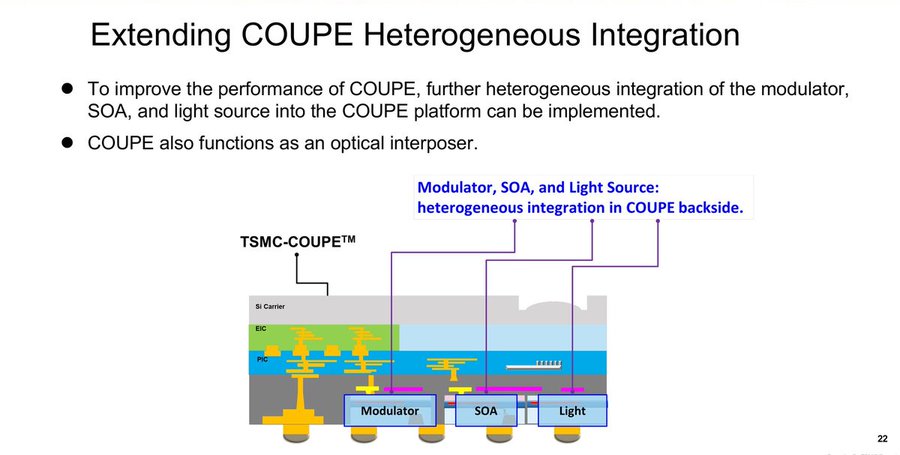
图 10|TSMC:COUPE 的进一步异质集成——把调制器、半导体光放大器(SOA)与光源集成到 COUPE 的背面;COUPE 同时也可作为光学中介层使用。
COUPE also works as an optical interposer, and TSMC will work out with customers how it integrates with CoWoS, the 2.5D packaging that puts the GPU and its HBM on 1 interposer.
UMC Lithium Niobate
UMC is Taiwan’s other foundry, the one that runs specialty and trailing-edge processes, and it has run silicon photonics in production since 2012, on 8-inch wafers with 12-inch ramping. Its claim is that nothing on silicon gets to 400G per lane by brute force.
Today’s 200G-per-lane pluggable is a known recipe: PAM4 modulation, a silicon Mach-Zehnder modulator, a DFB laser (distributed feedback, meaning it emits 1 clean wavelength), a germanium photodetector, a silicon-germanium driver and amplifier, and a DSP. At 400G per lane most of that recipe is in trouble. Germanium photodetectors need 110 GHz of bandwidth and are marginal, and the silicon-germanium transistors need a 500 GHz cutoff frequency. The industry has started drafting a 300G-per-lane bridging spec, which nobody would propose if 400G were on track.
The UMC speaker said silicon modulators are completely out of steam above 200G, and each fails for its own reason. The silicon Mach-Zehnder has a diode in it, because silicon changes its optical properties only when you inject or deplete charge. The diode’s capacitance limits the modulator’s electrical bandwidth, and the modulator needs 4 V of drive at 200G. The rule of thumb is 8 V at 800G, which the UMC speaker does not think a circuit designer can deliver. The micro-ring modulator is small and low voltage. However, it is sensitive to temperature within 1°C, it has the same diode, and it trades extinction ratio against speed, so the signal gets blurrier as the data rate rises. The electro-absorption modulator is also small, but it is lossy and it smears the pulse (dispersion), so it cannot reach far.
Beyond silicon, the UMC speaker said indium phosphide modulators are wonderful and very expensive. Organics, graphene and lithium tantalate are stuck at what he called the chicken-and-egg moment.
However, thin-film lithium niobate is past that moment. Bulk lithium niobate modulators ran the telecom industry for decades, so the reliability question is settled. Lithium niobate surface acoustic wave filters for phones then boomed in the late 2010s, which made lithium-niobate-on-insulator (LNOI) substrates an established industry, and optical-grade LNOI is available now. UMC started its TFLN line in 2021. The line has 6-inch qualified and in production at high yield, and it is sampling 8-inch. The device is X-cut lithium niobate (the crystal orientation that puts the electric field in the plane of the wafer) on silicon-on-insulator. That said, the modulator is centimeter-scale and the substrate is expensive. The modulator is also hard to integrate with the rest of the photonic circuit.
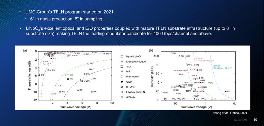
图 11|UMC:TFLN 的性能坐标。左图为相移器损耗(dB)随半波电压的变化,右图为带宽(GHz)随半波电压的变化;绿线为 TFLN 的 3 V / 6 V / 10 V 参考。数据源 Zhang et al., *Optica 2021。*
Still, TFLN wins on supply. Indium phosphide is scarce because it is the material that emits light, so every laser competes for it. By contrast, lithium niobate cannot emit light, so lasers do not compete for it.
The UMC speaker expects 2 more techniques to push bandwidth past what the modulator alone delivers. The first is coherent-lite. Full coherent optics reads data out of the phase of the light by mixing the incoming signal with a reference laser, called a local oscillator, and coherent-lite keeps the phase modulation but skips the polarization dimension. It is coming to short reach because of optical circuit switches, which reroute whole fibers of light without converting them to electrical signals. A switch costs 3 dB of the light in the link, and the local oscillator amplifies the signal enough to give the 3 dB back. TFLN is the modulator for coherent-lite because of its linearity. The second technique is wavelength-division multiplexing through micro-rings, which is creeping into CPO. Once it lands, the data rate per fiber goes up 4x in 1 generation, so he expects bandwidth to scale in jumps.
imec Silicon Photonics
imec is the Belgian research institute where much of the semiconductor industry’s process work is done before it reaches a foundry, and it runs a silicon photonics line that foundries license from. imec thinks 2026 is the year silicon becomes the dominant photonics platform, because silicon brings CMOS compatibility, volume, reliability and advanced packaging with it. At 200G per lane the platform is silicon plus silicon nitride plus germanium. The move from 8-inch to 12-inch wafers is under way, because 12-inch gives access to through-silicon vias and microbumps for advanced packaging. 12-inch also brings better lithography, which puts a micro-ring’s resonance wavelength under sub-nanometer control.
imec is pushing silicon as far as it goes. Its silicon modulator reaches 75 GHz, and 110 GHz at the 6 dB rolloff point, so it delivers an integrated 400G if nothing else is ready. imec’s germanium photodetectors have already demonstrated more than 110 GHz, and contrary to UMC, imec thinks germanium reaches 400G and beyond. imec has also redesigned its germanium-silicon electro-absorption modulator to run past 110 GHz and 400G for short-reach CPO.
imec’s stage 4 work is the optical interposer, for what it calls scale-in, the network below the rack and inside the package. A passive optical interposer carries silicon nitride waveguides across the whole 300 mm wafer, with XPUs and HBM hybrid bonded on top. A waveguide that runs across a whole wafer has to cross the boundaries between lithography exposure fields. imec has shown that stitching across those boundaries leaves no detectable defects, and waveguide loss is 0.1 dB/cm across the wafer, with 0.01 dB/cm in a recent result.
The connection from waveguide to waveguide through the hybrid bond, across a silicon carbon nitride interface, costs 0.2-0.3 dB per coupling at 2 microns of overlay accuracy, and the target is under 0.1 dB as the bonding tools improve. The remaining loss comes from bonding defects rather than from misalignment. Optics does not remove the reason the HBM sits next to the XPU, which is latency. However, imec’s simulations show optics beating copper on insertion loss (the signal lost in the link) even at that shortest distance, once the electro-optic devices are far more efficient than silicon’s.
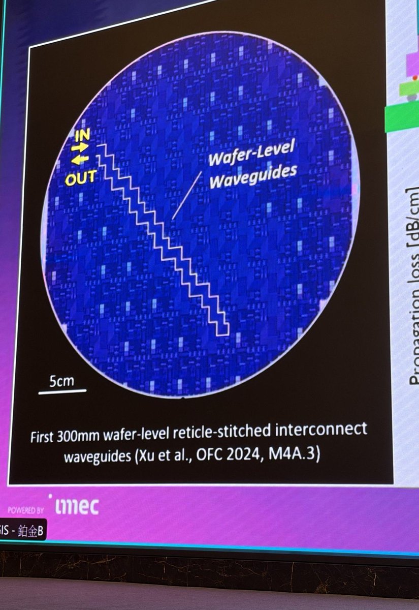
图 12|imec:首例 300 mm 晶圆级、跨曝光场拼接(reticle-stitched)的互连波导,贯穿整片晶圆(Xu et al., OFC 2024, M4A.3)。
Silicon is not an efficient enough modulator to beat copper over interposer distances, so imec is developing 3 alternatives. The first is barium titanate on silicon nitride. The second is a III-V modulator. III-V materials are the compound semiconductor family that includes indium phosphide and gallium arsenide, and they need 3-4x less drive voltage per unit of modulator length than silicon. The third is a plasmonic modulator from the startup Polariton, for beyond 400G. All of them arrive by microtransfer printing, which lets imec mix materials on 1 layer, use only as much lithium niobate or indium phosphide as the device needs, and reuse the donor substrate. imec already prints TFLN this way. A finished lithium niobate device is picked up and stamped onto the silicon wafer at the end of the line, because lithium is not welcome inside a CMOS fab, and the approach has produced 212.5 Gb/s with overlay accuracy under 0.5 microns.
Soitec Substrates
Soitec sits at the bottom of this value chain, making the silicon-on-insulator (SOI) wafers the photonic chips are built on. Its core process is SmartCut, which slices a thin single-crystal layer off 1 wafer and transfers it onto another. Soitec’s standard photonics SOI wafer holds the top silicon thickness to 1.4 nm from wafer to wafer, and under 1 nm on custom programs.
Soitec’s rack timeline matches Lightmatter’s. Today’s rack is 100% copper, with tens of XPUs sharing memory. In 2027-2028 the scale-up domain goes hybrid, with copper inside the rack and optics between racks. From 2029 the rack is 100% optical and compute and networking are disaggregated.
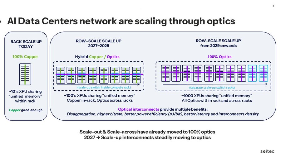
图 13|Soitec:AI 数据中心网络经光学扩展的三段路线图。今天机架内 100% 铜(约 10 颗 XPU 共享统一内存);2027–2028 转为混合(机架内铜 + 机架间光,约 100 颗 XPU);2029 起全光(约 1000 颗 XPU,计算与网络解耦)。
Soitec expects the optical engine to deploy in all 4 positions at once (pluggable, NPO, CPO and optical I/O), and NPO is the new one ramping for scale-up. However, Soitec’s destination is the photonic interposer, its version of optical I/O: an active silicon photonics interposer at package scale that connects the chiplets. It extends the shoreline, meaning the die edge length available for I/O. It also shortens the copper runs, which cuts latency and power, and it lets memory sit away from the logic chiplets. Because the interposer is active, it can also switch light to reconfigure the connections between chiplets.
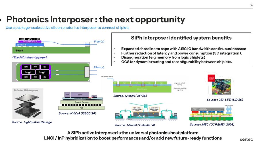
图 14|Soitec:光子中介层(Photonic Interposer)是下一个机会——用封装级有源硅光中介层连接 chiplet,可扩展 shoreline、降低延迟与功耗、把内存移出逻辑 chiplet,并支持通过切换光路重构 chiplet 间连接。
Soitec has 3 product lines. Photon-SOI is in full production at 200 and 300 mm. Soitec’s 200 mm fab is full with photonics and its 300 mm fabs are expanding, and the Singapore fab started shipping photonics SOI in volume in Q2 2026. Photon-LNOI is ramping, with 150 mm sampling now and 200 mm samples in early 2027, and Soitec said LNOI reaches 400G per lane at 15% lower power than silicon. Soitec’s 10-15 LNOI partners split between 2 wafer types. Thin-box wafers have 0.5-2 microns of buried oxide, for transferring lithium niobate onto SOI by wafer bonding or microtransfer printing. Thick-box wafers have 4-10 microns, for standalone TFLN circuits.
The third line, InPOSi, is an indium-phosphide-on-silicon substrate in R&D, and it is a supply play, because an indium phosphide seed layer on oxide on a high-resistivity silicon handle yields several wafers from 1 indium phosphide bulk crystal. It also bows less and conducts heat 3x better than bulk indium phosphide, and partners already have devices on it.
Lasers
I think the laser is the tightest supply constraint I saw at the conference. The laser makers split between indium phosphide (InP) lasers and gallium arsenide VCSELs for scale-up. A VCSEL (vertical-cavity surface-emitting laser) emits light straight up out of the wafer rather than out of a cleaved edge, so it is cheap to build in dense arrays.
Lumentum Lasers
Lumentum’s was the most interesting of the laser talks, because Lumentum, the largest indium phosphide laser maker, spent much of its time selling gallium arsenide VCSELs for scale-up. Lumentum also supplies the ultra-high-power laser inside NVIDIA’s Spectrum-X CPO switch.
On the indium phosphide side, Lumentum’s ultra-high-power laser is a 400 mW device with 20% wall-plug efficiency (20% of the electrical power in comes out as light), narrow linewidth and low noise, and it comes from Lumentum’s long-haul pump laser technology. Every extra milliwatt per laser removes ELSFP modules from the switch faceplate. At OFC 2026 Lumentum scaled the laser in 2 directions. The first is a 16-channel DWDM version at 350 mW per laser, which holds each wavelength within 25 GHz on a 200 GHz grid. The second is a single laser above 1 W at 25°C. When asked whether laser power keeps climbing once lasers are integrated onto the chip, the Lumentum speaker said integrated lasers will be a different product, because the economics that push a discrete laser’s power up disappear once the laser is inside the chip.
The VCSEL case starts from scale-up, where bandwidth per GPU doubles every GPU generation. Blackwell has 7.2 Tb/s of scale-up bandwidth per GPU, a 72-GPU domain and a 120 kW rack. Rubin has 14.4 Tb/s and 144 GPUs. Feynman has 28.8 Tb/s, with domain size and rack power still unknown. The Lumentum speaker said scale-up bandwidth, domain size and rack power are all fighting each other, and that only high-volume optics breaks the constraint.
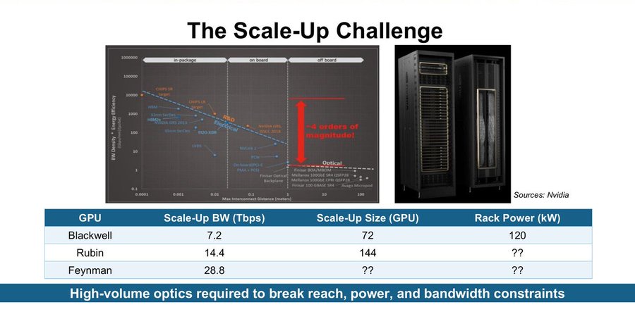
图 15|Lumentum:Scale-up 的挑战。左图为带宽密度·能效随最大互连距离的下降曲线(光学比铜高出 5 个数量级);右下表列出 Blackwell / Rubin / Feynman 的 scale-up 带宽、域大小与机架功耗。
Lumentum rates the VCSEL strong on 5 of 7 axes (speed, volume, power, reliability and density) and neutral on cost and reach. It rates silicon photonics strong on 4, and neutral on cost, power and reliability, because silicon photonics needs an external laser. Indium phosphide and TFLN come out weak on volume, cost and density. Gallium arsenide also wins on supply chain, because gallium arsenide wafers are available from many suppliers and indium phosphide wafers are more constrained. Lumentum said indium phosphide and the VCSEL serve different ecosystems. Indium phosphide pairs with silicon photonics and multi-wavelength links, while the VCSEL is for customers who do not want to work in silicon photonics.
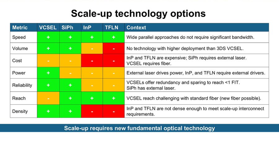
图 16|Lumentum:scale-up 技术选项评分矩阵。VCSEL 在速度、量产性、功耗、可靠性、密度五项最优;SiPh 在速度、量产性、可靠性、传输距离占优;InP 与 TFLN 在量产性、成本与密度上偏弱。
The technical case for the VCSEL is that other industries have already paid for its volume and its reliability. 3D sensing (face unlock on phones) took gallium arsenide VCSELs to volumes far above anything interconnect has run, and Lumentum alone has shipped more than 2b emitter arrays, or more than 10b individual emitters. Automotive LIDAR then solved high-temperature reliability. In 2025 Lumentum pushed the VCSEL to 1060 nm, where gallium arsenide is transparent enough that the emitters and detectors can be stacked directly on electronics and interposers.
Lumentum’s concept chiplet uses that stacking. It sits on the standard UCIe die-to-die interface and carries 8 transmit and 8 receive bundles of 64 channels each, for 32 Tb/s bidirectional. The VCSELs and photodetectors are stacked on top, and they run above 150°C with more than 5,000 hours of reliability data. Lumentum developed gallium arsenide photodetectors, so the whole receive side stays on the same supply chain, and Corning built an 80-core hexagonal fiber bundle with 30 m of reach to match the emitter array. In the OFC demo, 1060 nm VCSELs ran on an advanced CMOS chip at 32 Gb/s per channel, error free, under 2.5 pJ/bit, and VCSEL-on-ASIC at a 40-50 micron pitch is available now. Micro-LEDs are the other dense emitter for scale-up, and Lumentum puts VCSELs at 32-64 Gb/s per channel against 3 Gb/s for a manufacturable micro-LED.
Lumentum also builds a MEMS optical circuit switch, which steers light with microscopic tilting mirrors. It is a 300x300 port device with under 2 dB of loss across all ports, and its return loss is high enough for the bidirectional links the OCI MSA specifies. It is aimed at replacing spine switches and at failover. Lumentum said it cuts front-end and scale-out network power by more than 65% in 100K-GPU deployments.
Coherent VCSELs and Optical Switching
Coherent is the other big laser and transceiver maker, and it splits the laser market into the same 2 camps as Lumentum, with more weight on the VCSEL side. Coherent has shipped 1b VCSEL devices, and its VCSEL emitter count is over 200b. It demonstrated 200G-per-lane VCSELs at OFC 2025. On the indium phosphide side, Coherent has shipped 250m lasers and is moving production to 6-inch wafers. It has also shown a 400G differential electro-absorption modulated laser, and a 1.6T transceiver that uses its own indium phosphide continuous-wave laser and silicon photonics.
Coherent ranks every position the optical engine can take (retimed pluggable, linear pluggable, NPO, socketed CPO and soldered CPO) on channel loss, power, pluggability, serviceability and density. NPO and socketed CPO come out best, because they keep serviceability without giving up density.
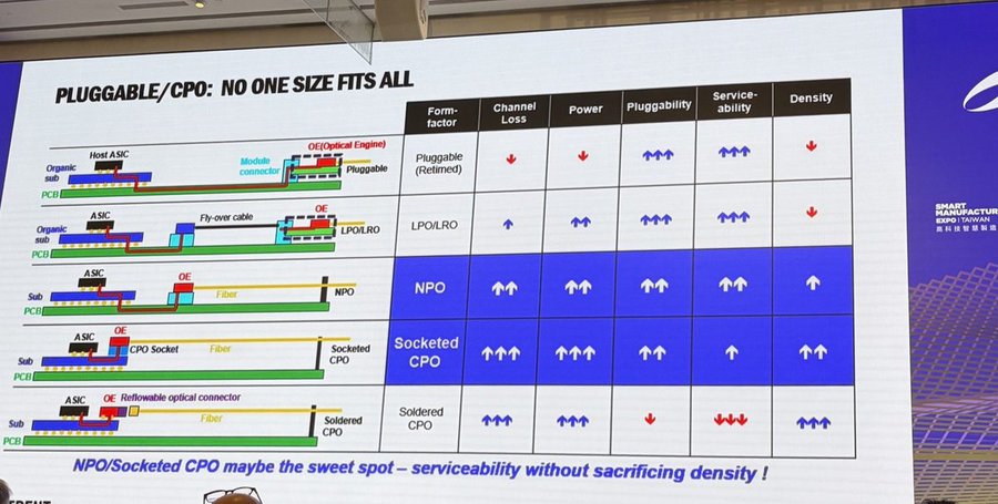
图 17|Coherent:可插拔与 CPO 各形态的权衡——从 retimed / linear 可插拔、LPO/LRO、NPO、socketed CPO 到 soldered CPO,按通道损耗、功耗、可插拔性、可维护性与密度打分;NPO 与 socketed CPO 在不牺牲密度的前提下保留了可维护性。
VCSEL-based CPO is low power, low cost and dense, and Coherent’s reference design is an 8x800G VCSEL CPO that it built with IBM. However, VCSEL CPO is short reach, while silicon-photonics CPO uses single-mode fiber for longer reach and larger networks.
CPO also changes the component market, because parts that used to be buried inside a transceiver become standalone products. Those include high-power continuous-wave lasers, ELSFPs, micro-lens arrays, fiber attach units and polarization-maintaining fiber.
Coherent’s optical circuit switch uses liquid crystal instead of MEMS mirrors, so it has no moving parts and no high-voltage components. The liquid crystal cells have shipped into subsea systems for more than 10 years, so their reliability record already exists.
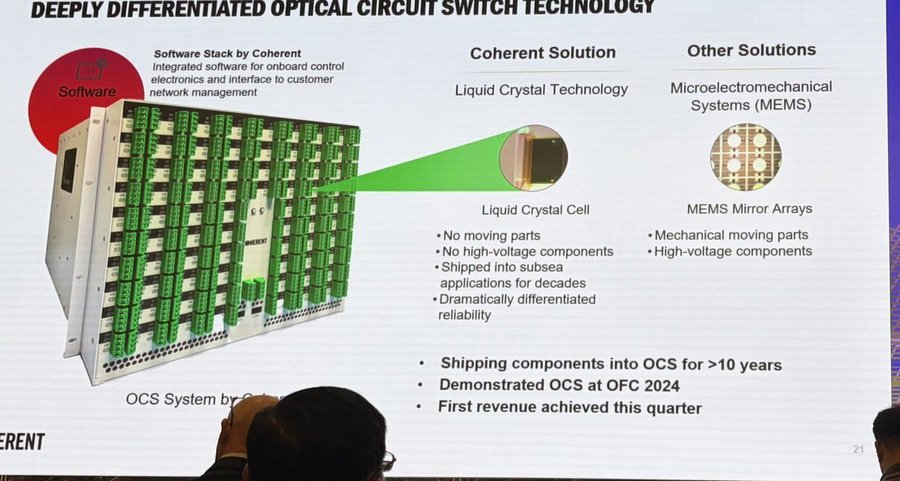
图 18|Coherent:光路交换(OCS)技术路线。液晶方案无运动部件、无高压元件,其液晶单元已入海缆应用十余年;MEMS 方案则有运动部件与高压元件。
Coherent demonstrated the switch at OFC 2024, and the switch took its first revenue this quarter.
SMART Photonics InP Chips
SMART Photonics is an independent indium phosphide foundry in Europe. Indium phosphide is the only material that does everything on 1 chip: lasers, optical amplifiers, amplitude and phase modulators, photodetectors, the passive waveguides between them, and a tunable laser as the local oscillator for coherent detection. SMART’s case is that a monolithic indium phosphide chip therefore avoids the hard step of coupling light between chips.
SMART offers a PDK of 50 components, customers design the chip, SMART runs the fab from epitaxy to grinding, and an OSAT (an outsourced assembly and test house) does the packaging. Production is on 4-inch wafers with deep-UV lithography, so the laser gratings are not written by e-beam. SMART and PhotonDelta are building a 6-inch pilot line, which is scheduled to run in early 2028.
SMART’s 2 building blocks are a laser and a modulator. The laser is a 400 mW DFB at 5°C, and SMART sells it as the light source for silicon photonics and CPO. The modulator is a 110 GHz device that SMART has tested to 480G per lane. It runs at high temperature without cooling, because cooling would spend the power the modulator saves.
SMART has a concept chip for each tier. For scale-up, an external laser module puts 64 wavelengths on 1 chip (8 ports, 8 wavelengths each, DFBs plus amplifiers) and packages as an ELSFP. For scale-out, a WDM transmitter carries 8 lasers, 8 modulators and a multiplexer at 200G or 400G per lane. For scale-across, a coherent transmitter combines a tunable laser, an IQ modulator (which writes data onto both the amplitude and the phase of the light) and an amplifier on 1 test chip, and putting the 3 together cost no measurable performance.
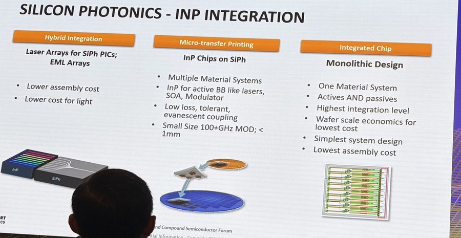
图 19|SMART Photonics:InP 与硅的三种集成路线。混合集成(激光阵列贴在 SiPh 芯片旁,光成本最低)、微转印(把 InP 薄膜转移并贴合到硅波导上,<1 mm 调制器)、单片集成(单一材料体系,集成度与装配成本最优)。
There are 3 routes to integrating indium phosphide with silicon. Hybrid integration puts a laser array next to a silicon photonics chip, at the lowest cost of light. When asked what limits the hybrid route, SMART’s CTO said chip-to-chip coupling at nanometer accuracy. Microtransfer printing, which SMART developed with imec, under-etches a thin indium phosphide membrane, picks it up with a stamp and places it on a silicon waveguide. The light crosses into the silicon through a nanometer gap without any lens in between, and the epitaxy sets that vertical gap, so only 1 axis of alignment is left. The printed modulator fits in under 1 mm, and the indium phosphide donor substrate is reused, which is how printing answers indium phosphide’s scarcity. Monolithic integration uses 1 material and has the lowest assembly cost.
Manufacturing
The optical engine also has to be packaged and built in volume. ASE packages it, and Lam makes the process tools for the photonic chip.
ASE Packaging
ASE is the largest OSAT. It packages chips for the fabless companies and increasingly takes the foundries’ overflow, so it will package a large share of the optical engines.
AI packaging asks for 2-10x improvements in memory, area, power and thermal, and a silicon interposer big enough for what AI needs becomes a problem in itself. ASE’s answer is fan-out redistribution layers (RDL) stacked on a substrate. ASE’s FOCoS and FOCoS-Bridge are the equivalents of TSMC’s CoWoS-R and CoWoS-L. The platform runs 3 to 12 RDL layers in prototype and 15 in development. Lines in the bridge are 0.4 microns, and I/O density is 50x a flip chip package, or 200x with the bridge. Panel-level packaging, which builds the same structure on a large rectangular panel instead of a round wafer, gets 36-49 units of a 7.5-reticle device from a 600 or 620 mm panel against 6 from a 12-inch wafer.
The optical engine is 20-100x smaller than a pluggable, so it can move from the edge of the board to under the edge of the package. ASE said the engine delivers 16-32x the performance of a pluggable at 6x lower power, with recent demonstrations at 12-15x and up to 30x. Engine construction runs from wirebond, which is still in use, through flip chip, to fan-out package-on-package. The fan-out version has no through-silicon vias and serves lower lane rates. However, lanes above 200G need a 3D stack with vias in the electronic or photonic die.
Coupling loss targets of 0.3 dB hold at 4 or 16 channels and become 1, 1.5 or 2 dB at 40, because fiber pitch and integrated mirror angle vary across the array. ASE wants to test every die at wafer level before it is packaged, which is known-good-die testing. However, the testers weigh 6-8 tons, so a fab can place 1 of them rather than 10 or 20. ASE is pushing for a common interface standard across the supply chain through the CPI consortium, which has grown from 30 to more than 150 members.
Lam Research Process Tools
Lam Research is the deposition, etch and clean tool vendor, and its specialty technology group covers photonics alongside power and sensors.
Silicon nitride deposited by plasma at low temperature traps hydrogen, and the hydrogen makes a waveguide lossy around 1550 nm (the C-band) and even around 1310 nm (the O-band). Lam is therefore running low-temperature, low-hydrogen plasma deposition at several leading customers now, and it is developing pulsed laser deposition as the next step. Pulsed laser deposition ablates a 100 mm target with an excimer laser into a plasma the size of an apple and sweeps it across the wafer, so whatever is in the target lands on the wafer with nothing added. A hydrogen-free target therefore gives a hydrogen-free film, at under 200°C or even room temperature, with the tight control of thickness and refractive index that a waveguide layer needs. The technique is at the feasibility stage, and Lam targets customer demos for early 2027. Lam said its early loss data is the best it has seen from any nitride process, although that data comes from bulk transmission rather than from customer test structures. The same tool can also deposit barium titanate, the high-speed electro-optic material imec and others want for modulators. Barium titanate has no chemical etch at all, so it is etched purely physically by ion beam, a process already in production for barium titanate optical switches.
Etch fights roughness and pattern density. Waveguide sidewall roughness is 1-2 nm today, and the goal is under 1 nm. Photonic layouts also swing between extremes of pattern density, because a micro-ring is a wide open area next to a gap of a few hundred nanometers, and that gap sets the device’s performance. Grating couplers add blind etches with no stop layer. As a result, etch on a 45 or 65 nm photonics node is as hard as anything on a leading logic node, and it takes the high-voltage pulsing developed for leading-edge etch.
By contrast, fiber coupling looks like MEMS work. Deep cavities, trenches, through-silicon vias and metalenses are etched on a deep reactive ion etch tool, and those deep back-end etches damage the wafer’s edge, so Lam’s bevel tool protects or rebuilds the edge to save yield. In packaging, Lam’s electroplating and clean tools fill fan-out features from 5 micron lines to 150 micron pillars. For hybrid bonding, Lam supplies the nitrogen-doped silicon carbide interface layer and the copper grain engineering that decide bond strength.
Test
The morning was foundries, laser makers and interconnect companies pumping up CPO, and the afternoon was the test vendors saying to hold your horses.
Onto Innovation Process Control
Onto Innovation is a process control vendor. It sells the inspection and metrology tools that measure what a fab has just made, and it has more than 10,000 tools in the field.
Onto’s AI defect classifier trains only on the customer’s own data. Its analytics layer combines the defect map with electrical test to decide the fate of borderline dies, which cuts false scraps.
Onto has organized its photonics work around 5 problems: fiber attach, gratings, facets, laser mesas and micro-lenses. For fiber attach in a V-groove, Onto measures the groove’s dimensions, sidewall angle and surface defects down to 150 nm, plus the vents that let gas escape when the fiber is glued in. For gratings it measures profile, trench depth, sidewall angle, cladding thickness and refractive index on 1 tool. A waveguide facet’s angle decides reflection and coupling efficiency, whether the facet is made by dicing or by etch, and Onto resolves a change of 0.06 degrees in that angle. On the mesa of an edge-emitting laser, trench depth decides polarization behavior.
Micro-lenses are becoming more common because they relax the alignment tolerance of the whole package and cut its cost. However, any defect on the lens surface, or a missing lens, turns into optical loss and channel imbalance. Wafer bow and stress, which packaging has always measured for mechanical reasons, are now optical problems too, because stress shifts what the waveguide does.
Onto’s 2026 problems are on the wafer: evanescent coupling (light crossing a gap between 2 waveguides), cladding uniformity, sidewall profile, micro-lens shape and V-groove quality.
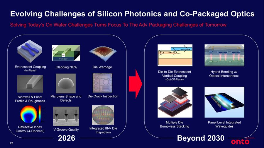
图 20|Onto Innovation:硅光与 CPO 挑战的演进。2026 年集中在晶圆级问题(近场耦合、包层均匀性、晶圆翘曲、侧壁/端面粗糙度、微透镜缺陷、折射率控制、V 型槽质量、III-V 裸片检测);2030 年后转向键合界面的光学耦合(跨界面近场耦合、带光学互连的混合键合、无凸点多裸片堆叠、面板级集成波导)。
Beyond 2030, the problems are all about optical coupling across a bonded interface: die-to-die evanescent coupling out of plane, hybrid bonding with optical interconnect, multi-die bump-less stacking and panel-level integrated waveguides.
ficonTEC Test Equipment
ficonTEC is a German maker of photonic assembly and test equipment with about 100 people. It has shipped 2,000 tools in its 25 years, and it needs to ship 1,000 more in the next 12-18 months. That takes more factories, and it takes people with skills the semiconductor industry does not have, in photonic device engineering, optical alignment and fiber handling. To get there, ficonTEC designs in Germany and builds in Taiwan, under an exclusive photonics partnership.
Test gets harder with every step up in bandwidth and integration, because the device is now a system, with a GPU, HBM, electronic dies, photonic dies, lasers and fibers all in 1 package. Test therefore has to follow the device from wafer to chip to module.
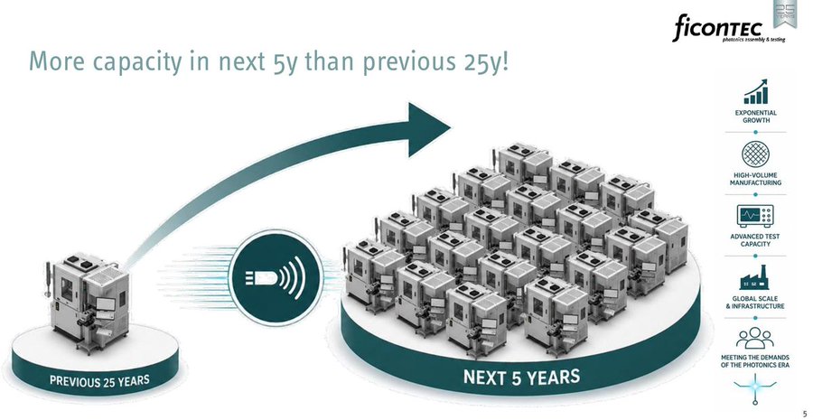
图 21|ficonTEC:未来 5 年的产能需求将超过过去 25 年的总和——25 年累计交付 2,000 台,而未来 12–18 个月就要再交付 1,000 台。
ficonTEC’s test flow has 4 insertions, and it maps onto TSMC’s COUPE. Insertion 1 tests the electronic and photonic wafers separately from the top side. Insertion 2 comes after the micro-lens array is bonded to the photonic wafer. The wafer is flipped and tested electrically from the top and optically from the bottom through the lenses, and the fiber array is held 100 microns away and never glued. Insertion 3 tests the singulated die through a pre-attached receptacle, with a test connector that does not click in. Insertion 4 tests the module. The cost of a failure climbs 1x, 10x, 100x and 1,000x through the 4 insertions, so the flow is designed to find failures early. Correlation and traceability run between every insertion, because a field failure has to be traceable back to the wafer.
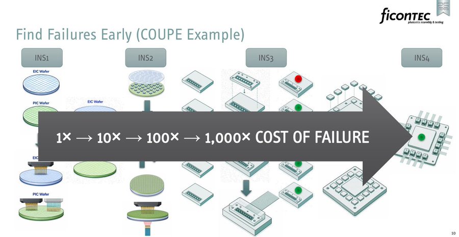
图 22|ficonTEC:以 COUPE 为例的四次插入(Insertion)测试流程——失效代价沿 INS1→INS4 依次放大 1x → 10x → 100x → 1,000x,因此测试流程的设计目标就是尽早发现失效。
ficonTEC has a tester for each insertion. The single-sided wafer tester ships now. It cleans lenses by laser and trims the refractive index of waveguides and rings by laser, which raises yield and cuts the power spent on thermal tuners. The double-sided wafer tester has a chuck that holds temperature within 0.5°C, a profiling system for the heavy warpage of stacked wafers, and a fiber array on the bottom side, and it works with Teradyne now and Advantest next month. The double-sided die tester has run at an OSAT for more than 6 months and tested more than 250K devices at 224G. Dirt on the socket is its biggest problem.
The module tester tests 12 to 36 engines in parallel. It has multiple thermal zones, 2-3 kW of heat removal at the center and high compression force, and hundreds of fibers that have to be inspected and cleaned at every connection. The production version ships to an OSAT at the end of September at 1.6T, and it runs fully robotic in a dark fab. Lead times are 12-16 weeks when a customer gives a forecast, and the constraint is pre-buying long-lead material.
Advantest Test Equipment
Advantest is 1 of the 2 big automated test equipment (ATE) vendors, the makers of the machines that electrically test every chip before it ships, and it is building the photonic version of that business. How the electronic die is bonded to the photonic die decides whether the wafer can be probed from 1 side or 2, and that decision sets Advantest’s whole flow. An edge-coupled COUPE can be tested single-sided, and a grating-coupled one needs double-sided electro-optical probing. Insertion 1 measures electrical parameters and optical DC, meaning power and dark current, and modulation testing moves in from insertion 2.
3 problems are common to all 4 insertions. There is no standard way to align an optical probe fast, accurately and repeatably. There is no standard detachable optical connector either, so the module-level test has to handle 1 connector on 1 side for NPO and N connectors on multiple sides for CPO. Finally, optical instrumentation is still rack-and-stack, easy to customize and hard to duplicate, while channel counts can double within 6 months.
Advantest works with a partner at each level of the flow. At wafer level, its V93K Triton tester pairs a 6-axis active alignment stage from the CM300 prober family with a standardized optical rack, and Advantest’s SmarTest software controls both. The tester reaches 0.1 dB of stability because its test head is water cooled and engineered against vibration. JenOptik (passive alignment) and Technoprobe (active, 3 axes) are proving probe cards, and a 6-axis edge-coupler result reached 0.3 dB stability this year. FormFactor does the double-sided wafer probing and targets high-volume qualification for mid-2027. At die level, test runs on an MPI DT650 with Marvell at 0.1 dB, and it qualifies in early 2027. At module level, the optics are tested by optical loopback and the electrical side by the switch or GPU ASIC itself, because no ATE handles 400G+ digital signals cheaply. An optical door fixture mates the connectors automatically on press-down.
The Advantest speaker wants the industry to move to higher-power lasers that feed more channels, and to denser optical instruments built into the ATE with their own calibration.
Spectral Imaging for CPO Yield
Insertion loss and reflectometry are scalar measurements. If 100 photons go in and 30 come out, you know 70 were lost among the modulators, waveguides and couplers, but not where. Spectral imaging is a yield tool that shows where.
It puts a wavelength-selective element between the microscope optics and the image sensor, so light leaking out of the circuit is mapped in space for each wavelength. It retrofits onto existing probe stations from MPI, FormFactor and ficonTEC. In the first validation example, an imaged hotspot on an arrayed waveguide grating was cut open by focused ion beam and traced to an irregular sidewall angle at 1 grating element. In the second, a leak in a taper was traced under an electron microscope to a defect that is invisible optically. In a wafer screening test across 68 dies, the image-based pass/fail matched the Keysight insertion-loss result and ran 6x faster. An extinction ratio read from the image also matched the conventional measurement on a Mach-Zehnder.
Photonic yield also drops when the electronic die is bonded on. Thermal stress, polishing and mechanical force shift the waveguides, and by TSMC’s figure a 1 nm change in a waveguide’s critical dimension shifts its center frequency by 100 GHz. Optical known-good-die is therefore harder than electrical known-good-die, which is pass or fail, and the speaker proposed a risk ranking for photonic dies instead, where a model combines the images with conventional test data to predict which dies will fail downstream.
Conference Takeaways
Scale-Up Domain Size
I think Lightmatter gave the most important talk of the conference, because most of the conference was building stage 2 and Lightmatter showed what stage 2 buys. At the same power, a 512-GPU optical scale-up domain trains a trillion-parameter model 3x faster than 4 copper pods of 144. It also serves the first token of a 131K-token prompt 3x faster, and it generates tokens 2x faster per user.
None of that depends on Lightmatter’s engine. The gain comes from removing the pod boundary, where every transfer drops to scale-out bandwidth, so it would hold with NVIDIA’s engine in the link.
Optical I/O vs CPO
Several presenters separated optical I/O from CPO, and I had not seen that at 1 event before. TSMC drew the line formally, with CPO-MCM (the engine on the substrate next to a switch) and CPO-OOI (the engine on the XPU’s interposer), and it put optics on interposer at 10x copper’s energy efficiency and under 0.05x its latency, against 4x and under 0.1x for CPO. Soitec introduced its solution for optical I/O, the photonic interposer, and imec showed the pieces of one, with wafer-scale silicon nitride waveguides and waveguide-to-waveguide hybrid bonding at 0.2-0.3 dB per joint. imec and Lightmatter both used a new word for the tier, scale-in. TSMC’s plan to integrate the modulator, amplifier and light source onto the back of COUPE, which also works as an optical interposer, is the platform version of stage 4, and Onto’s beyond-2030 roadmap is the metrology version.
What changes on the interposer is what the engine can reach. An engine on the substrate connects GPU to GPU. By contrast, an engine on the interposer can carry GPU-to-HBM traffic, and once that traffic is optical the HBM does not have to sit next to the GPU. This is what enables optical memory pooling (placing DRAM in entirely separate trays).
Modulators at 400G per Lane
UMC’s case by elimination runs through every silicon option, from the Mach-Zehnder’s 8 V drive at 800G to the micro-ring’s 1°C thermal window and the electro-absorption modulator’s short reach, and leaves thin-film lithium niobate or indium phosphide. Indium phosphide is in short supply, as Lumentum, UMC and Soitec all said, so I expect TFLN to carry scale-out modulation at 400G per lane. Several presenters converged on the same answer, and I did not hear serious pushback. Soitec’s LNOI wafers, UMC’s 8-inch TFLN line and imec’s microtransfer printing are the 3 pieces of that supply chain, and Marvell lists TFLN first for long reach.
The argument resolves by domain rather than by winner, because scale-up under the OCI MSA is micro-rings plus DWDM on silicon, where Lightmatter’s advice not to bet against silicon holds. Silicon is the host in both domains, and everything else is printed or bonded onto it, which is why microtransfer printing came up in 4 talks.
Lumentum and VCSELs
Lumentum is the largest indium phosphide laser maker and the supplier inside the first CPO switch, so it should be the company most favorable to the silicon photonics roadmap. However, it spent much of its talk on gallium arsenide VCSELs for scale-up, and it rated VCSELs strong on nearly every axis. I think that is a strange thing for Lumentum to do, because the VCSEL is the technology that could displace Lumentum’s indium phosphide business.
I think the most credible explanation is capacity. Lumentum’s indium phosphide is sold out for years, so there is nothing it can do to sell more of it. The VCSEL, which Lumentum has not yet sold into interconnect, is the only incremental revenue available, along with the driver, amplifier and packaging around it. Coherent, the other indium phosphide leader, also splits the market this way and has a VCSEL CPO reference design built with IBM.
Test Capacity
No part of the 4-insertion flow the test vendors described is standardized, and none of it is in full volume production yet. Known-good-die is harder in optics than in electronics, because bonding the electronic die shifts the waveguides enough to move their frequency by 100 GHz per nanometer. The yield problems still need physical failure analysis to explain.
Scale-up needs 10-100x the optical engine test of scale-out, and the testers that do it weigh 6-8 tons, so a fab can place only 1. ficonTEC needs to ship 1,000 tools in 12-18 months against 2,000 in its entire history, and it builds them in Taiwan because that is where the capacity is. Test capacity therefore sets the pace of stage 2 as much as any vendor roadmap does, and if the 2027 NPO date slips, I expect it to slip on test capacity rather than on the optics.
thanks for reading. if enjoyed, like repost and follow!
第二部分:中文结构化解读
本部分为本站独立撰写,其中的质疑、推算与判断均属解读者观点,不代表原文作者立场,也不构成投资建议。原文作者为 Jason’s Chips(@jasonschips),其文风为个人投资者视角,本站如实转载并在本节标出需要留意的口径问题。
速览
| 项目 | 内容 |
|---|---|
| 文章性质 | 会议综述,非论文、非公司深度 |
| 会议 | SEMICON Taiwan 2026(论坛自 8 月 31 日起,主展 9 月 2–4 日,台北南港展览馆) |
| 原文来源 | Jason’s Chips(@jasonschips)X 长文,发布于 2026 年 9 月下旬 |
| 覆盖讲者 | Marvell、Lightmatter、TSMC、UMC、imec、Soitec、Lumentum、Coherent、SMART Photonics、ASE、Lam Research、Onto Innovation、ficonTEC、Advantest,共 14 家 |
| 原文分类 | Networks / Foundries / Lasers / Manufacturing / Test / Conference Takeaways,六节 |
| 全篇张力 | 上午是代工厂、激光厂与互连公司推 CPO,下午是测试厂商泼冷水 |
| 最反直觉的两条 | ① 激光器是全会议最紧的供给约束;② 决定 stage 2 时间表的是测试产能,不是光学 |
| 最硬的数字 | Lightmatter 512-GPU 光域训练 3x 快、decode 2x 快;ficonTEC 要把 25 年 2,000 台的交付史压缩到 12–18 个月内再交 1,000 台 |
一句话核心
这篇综述的证据密度很高,但它的真正主张只有一句:从 stage 1 到 stage 4,光学要解决的问题已经不是「光够不够快」,而是「封装、激光供给与测试能不能跟上」——作者用一整天会议的五段结构把这句话从「网络收益(值得做)」推到「代工与材料(做得出)」,再推到「激光(供给最紧)」「封装(良率搬家)」,最后落在「测试(产能决定节奏)」上。
一、文章的坐标系:stage 0 → stage 4
原文开头给出了一把自己造的尺子,全篇的每个讲者都被放回这把尺子上。这是本文最值得先记住的部分:
| 阶段 | 定义 | 位置 | 状态 |
|---|---|---|---|
| Stage 0 | 可插拔光模块,用于 scale-out | 交换机前面板 | 早已完成 |
| Stage 1 | 同一批 scale-out 链路的 CPO | 交换机封装内 | 已出货 |
| Stage 2 | 机架之间的 scale-up CPO | 封装/板边(含 NPO) | 争论最集中 |
| Stage 3 | 机架内部的 scale-up CPO,替代铜 | 封装内 | 争论次集中 |
| Stage 4 | 光学 I/O(亦称 scale-in),光引擎移到 GPU 旁的中介层 | 中介层上 | 前瞻演讲落点 |
关键在 stage 4 的含义:光引擎一旦落在中介层上,它可以承载 GPU 到 HBM 的流量,于是 HBM 不必再紧贴 GPU——这就是「光学内存池化」的前提。原文这条线索很短,但它是整篇文章里唯一一个会改变系统架构而不只是改变链路的结论。
二、因果骨架
把原文的论证压成一条链:
- 集群变大 → 网络分层变多。GPT-5 用 5 万–10 万加速器训练,今天的模型用百万级加速器,对应千万级光互连。
- 每一层的流量放大倍数不同。相对广域接入带宽:传统数据中心前端 7x,AI 数据中心前端 14x、scale-out 56x、scale-up 500x——而 500x 那一层至今仍在铜上。
- 铜在那一层失效的原因是能量,不是带宽:可插拔 1.6T 已到 10 pJ/bit 并停止下降,因为模块内的 DSP 随速率同步变大;把光学搬进封装可删掉驱动信号过板的那一级 SerDes,这才是功耗改善的来源。
- 所以要往芯片里搬:可插拔 → NPO → CPO → 中介层光学,每往内一步,电学路径短一截,代价是工程复杂度与测试难度指数上升。
- 复杂度上升的结果是瓶颈转移:从「光够不够快」转到「激光够不够多」「良率与封装够不够稳」「测试够不够快」——这就是下半场(Lasers / Manufacturing / Test 三节)的全部内容。
三、分板块拆解
1. Networks:唯一给出可验证收益的一节
| 讲者 | 主张 | 证据 | 我的判断 |
|---|---|---|---|
| Marvell | 每个距离档位跑自己的调制格式;400G/lane 以上需要「又小又快」的调制器 | NRZ(机架内、10 m 内)/PAM4(scale-out 到 1.6T)/16-QAM 相干(scale-across);等离子体调制器实测 990 GHz,对比常规最好器件 110 GHz | 990 GHz 是单点实验室值,且作者点名「问时间表得到的回答是五年后再问」。把它当已解决的技术读会出错 |
| Marvell | CPO 会「反转」交换机前面板——外置激光模块(ELSFP)占掉大部分面板,整机水冷 | 两颗在产 / 往第四代走;32 lane × 224G;电学侧由系统级重路由处理冗余,micro-LED 则在硬件上切备用发射器 | 冗余由「系统重路由」承担还是「硬件备用」承担,取决于器件是否便宜到可以多备——这条差异会反过来决定 micro-LED 与硅光各自的适用域 |
| Lightmatter | 大 scale-up 域的收益与用谁的引擎无关 | 4×144-GPU 铜 pod(1.00x)vs 512-GPU 光域:训练 0.60x,带宽提到 32 Tb/s/GPU 后 0.37x;Prefill 首 token 快 3x,Decode 每用户 token 速率 2x | 论证成立但要注意口径:该对比同时改变了两件事——有无 pod 边界、以及 GPU 总数(576 vs 512)。0.60x 是两者叠加的结果,把它全部归因于「取消 pod 边界」略有跳跃。方向不受影响 |
| Lightmatter | OCI MSA 是第一个为光学而不是为 SerDes 写的标准;单纤双向(BiDi)是必然选型 | OCI 由 OpenAI、Broadcom、AMD、NVIDIA 等于 2026 年 3 月发起;BiDi 在 512 XPU 集群省 240 km 光纤、少 2 万个连接器与故障点、总网络开销降 16% | 「省 2 万个连接器」是本文少有的、可直接对应到运维成本的数字,价值高于同段的百分比 |
| Lightmatter | 激光器不能再靠单管加功率 | 100T 交换机需 16–18 个 ELSFP,800T 需 128 个;分立 InP 激光器已推到 400 mW,接近会烧毁光纤的功率 | 这是全篇供给侧论证的起点:带宽翻倍 ⇒ 激光器数量翻倍 ⇒ 成本与面积同比例翻倍。Guide 的 128 管/芯片就是对这个算术的回答 |
2. Foundries:200G/lane 以上,硅调制器集体出局
| 讲者 | 主张 | 证据 | 我的判断 |
|---|---|---|---|
| TSMC | 首次把 CPO 与光学 I/O 正式分成两个产品 | CPO-MCM(光引擎在基板,配交换芯片)与 CPO-OOI(光引擎在 XPU 中介层);效率 2x/4x/10x,延迟 1x/低于 0.1x/低于 0.05x(依次为可插拔/CPO/OOI,相对铜) | 这条是本文最有结构意义的切片,见下方「我的评述」第 3 点 |
| TSMC | 引擎带宽 = 单通道速率 × 通道数 × 波长数,两条路都要走 | fast-and-narrow 提单通道到 400G+,slow-and-wide 保持 200G 并加波长(1→4→8→16);两条路在 2026 年起都能到 3.2/6.4/12.8/25.6/51.2 Tb/s | 「两条路都不选」本身是一个策略信号:谁把接口定义权握在手里,谁就不用现在站队 |
| UMC | 硅上没有任何办法靠蛮力做到 400G/lane | MZM 的二极管电容限带宽、200G 需 4 V 驱动、800G 需 8 V;微环温漂窗口 1 ℃ 且以消光比换速度;EAM 有损且色散;行业已在起草 300G/lane 的过渡规范 | 「若 400G 在正轨上,没人会去提 300G 的过渡规范」是本文最锋利的一句反向推理 |
| UMC | TFLN 赢在供给,不是性能 | 6 英寸已量产高良率、8 英寸送样;LNOI 因手机声表面波滤波器而在 2010 年代后期成为成熟产业;铌酸锂不发光,所以激光器不与它争材料 | 这是一个非常实用的论证角度:材料之争也可能是供给之争,而非性能之争 |
| imec | 2026 年是硅成为主流光子平台的一年 | 8 英寸转 12 英寸;调制器 75 GHz(6 dB 滚降点 110 GHz);锗探测器已演示超过 110 GHz;晶圆级波导损耗 0.1 dB/cm,近期做到 0.01 dB/cm;混合键合波导对接 0.2–0.3 dB/耦合,目标低于 0.1 dB | 与 UMC 直接冲突(见下方「内部不一致」第 3 条) |
| Soitec | 机架时间表与 Lightmatter 一致 | 今天 100% 铜(约 10 颗 XPU);2027–2028 混合(机架内铜 + 机架间光,约 100 颗);2029 起全光(约 1000 颗,计算与网络解耦) | 两家独立来源给出同一时间表,比任何单家的路线图都更值得参考 |
| Soitec | 终点是光子中介层 | Photon-SOI 满产(200/300 mm,新加坡厂 2026 Q2 起量产出货);LNOI 150 mm 送样、200 mm 2027 初送样,称 400G/lane 且功耗比硅低 15%;InPOSi 在研,导热性比体 InP 好 3 倍 | Soitec 是这条链上位置最低(卖衬底)但最不依赖单一材料路线的一家——三条产品线正好覆盖硅、铌酸锂、InP |
3. Lasers:全篇最紧的供给约束,也是最反直觉的一节
| 讲者 | 主张 | 证据 | 我的判断 |
|---|---|---|---|
| Lumentum | 大部分时间在推 GaAs VCSEL,而不是自己的 InP | 评分表:VCSEL 在速度、量产性、功耗、可靠性、密度五项占优,成本与传输距离中性;InP 与 TFLN 在量产性、成本、密度上偏弱 | 作者说这件事「很怪」,见下方「我的评述」第 1 点 |
| Lumentum | VCSEL 的量产性与可靠性是别的行业已经付过钱的 | 3D 感知(手机面部识别)把 GaAs VCSEL 推到互连从未有过的量级,Lumentum 已出货超过 20 亿个发射器阵列(超过 100 亿个单发射器);汽车 LIDAR 解决了高温可靠性;2025 年推到 1060 nm,GaAs 在此波长透明到可以把发射器与探测器直接堆在电子器件与中介层上 | 这是全文最扎实的一段供应链论证:「已经量产」比「性能最好」更难复制 |
| Lumentum | InP 侧继续往上推功率,但集成后经济学改变 | 400 mW、20% 插墙效率;OFC 2026 推出 16 通道 DWDM 版本(350 mW/管,200 GHz 栅格内 25 GHz 精度)与 25 ℃ 下超过 1 W 的单管 | 「激光器一旦集成进芯片,就不再有把分立激光器功率往上推的经济学」——这句话意味着未来功率优化点会从激光器移到系统 |
| Lumentum | scale-up 带宽、域大小与机架功耗三者互相打架 | Blackwell:7.2 Tb/s/72 GPU/120 kW;Rubin:14.4 Tb/s/144 GPU;Feynman:28.8 Tb/s,域大小与机架功耗未知 | 把「未知」明确写出来,比填一个乐观假设更有价值 |
| Coherent | 市场分成与 Lumentum 相同的两派,但更偏 VCSEL | 已出货 10 亿个 VCSEL 器件、发射器总数超过 2000 亿;OFC 2025 演示 200G/lane VCSEL;InP 侧已出货 2.5 亿颗激光器并转 6 英寸;已演示 400G 差分 EAM 激光器与 1.6T 自有 InP CW 加硅光模块 | 与 IBM 合作的 8×800G VCSEL CPO 参考设计是这段的锚点 |
| Coherent | CPO 会把「埋在模块里」的零件变成独立产品 | 高功率 CW 激光器、ELSFP、微透镜阵列、光纤贴装单元、保偏光纤 | 这是整篇里最容易被忽略、但对选标的阶层最有用的一条结构性判断 |
| SMART Photonics | InP 是唯一能在一片芯片上做完所有事情的体系 | PDK 50 个器件;4 英寸产线用深紫外光刻(激光光栅不用电子束写);6 英寸中试线计划 2028 初;400 mW DFB(5 ℃);110 GHz 调制器已测到 480G/lane;三条与硅的集成路线(混合集成/微转印/单片) | 单片集成「省掉了芯片间耦合这一最难的步骤」是 InP 唯一的、无法被硅光复制的结构性优势 |
4. Manufacturing:良率问题从晶圆搬到了封装
| 讲者 | 主张 | 证据 | 我的判断 |
|---|---|---|---|
| ASE | AI 封装要求内存、面积、功耗、散热提升 2–10 倍;衬底中介层本身成为问题,答案是扇出 RDL | FOCoS/FOCoS-Bridge 对应 TSMC 的 CoWoS-R/L;RDL 3–12 层在原型、15 层在研;桥接线宽 0.4 微米;面板级封装从 600/620 mm 面板出 36–49 颗 7.5 倍光罩器件,12 英寸晶圆只出 6 颗 | 光引擎比可插拔小 20–100 倍,因此可以从板边移到封装边缘之下——尺寸差异是封装形态变化的物理原因 |
| ASE | 耦合损耗随通道数上升 | 0.3 dB 在 4 或 16 通道成立,40 通道变成 1、1.5、2 dB,原因是光纤间距与集成反射镜角度在阵列上不均匀 | 这是本文少有的「给出衰减曲线」的地方,可直接用来估算 40 通道以上的良率压力 |
| ASE | 想在封装前测试每一颗裸片,但设备太重 | 测试机重 6–8 吨,一个 fab 只能放 1 台而不是 10 或 20 台;CPI 联盟从 30 家增到 150 家以上 | 「设备重量」这种物理约束很少被写进研报,但它直接限制了 known-good-die 的产能 |
| Lam Research | 等离子体沉积的氮化硅会困住氢,使波导在 C 波段甚至 O 波段有损 | 已在多家领先客户跑低温低氢等离子体沉积;下一步是脉冲激光沉积(用准分子激光轰击 100 mm 靶材、在 200 ℃ 以下甚至室温成膜,无氢靶材给无氢薄膜),可行性阶段,目标 2027 初客户演示 | 「无氢靶材⇒无氢薄膜」的逻辑很干净,但作者也指出其早期损耗数据来自体透射而非客户测试结构——口径要留意 |
| Lam Research | 光子刻蚀的难度被低估 | 波导侧壁粗糙度今天 1–2 nm,目标低于 1 nm;微环旁边几百纳米的间隙直接决定器件性能;光栅耦合器需要无停止层的盲刻蚀,因此 45/65 nm 光子节点的刻蚀难度与领先逻辑节点相当 | 「光子节点刻蚀难度≈领先逻辑节点」是本文最重要的工艺结论之一 |
5. Test:上午吹、下午泼水
| 讲者 | 主张 | 证据 | 我的判断 |
|---|---|---|---|
| Onto Innovation | 良率工具要从「丢了多少」升级到「丢在哪里」 | 光谱成像在显微镜与传感器之间插入波长选择元件,把漏光按波长在空间上成像;在 68 颗裸片的晶圆筛选中,图像判定的通过/失败与 Keysight 插损结果一致且快 6 倍;一个阵列波导光栅的热点经聚焦离子束剖开后定位到某光栅元件的侧壁角异常 | 与标准测量「一致性 + 快 6 倍」是很少见的交代方式,比单说「更准」可信 |
| Onto Innovation | 光子 known-good-die 比电子更难,因为键合会移动波导 | 按 TSMC 的数字,波导关键尺寸变化 1 nm 会使中心频率移动 100 GHz;因此提出对光子裸片做「风险排序」而不是通过/失败二元判定 | 1 nm ⇒ 100 GHz 是全文最容易被记住的敏感度数字 |
| ficonTEC | 未来 5 年产能需求超过过去 25 年 | 25 年累计交付 2,000 台,未来 12–18 个月要再交 1,000 台;德国设计、台湾制造;模块测试机一次测 12–36 颗引擎,2–3 kW 中心散热,交付 lead time 12–16 周 | 换算成年化交付率是 8–12 倍(见下方「数值复核」) |
| ficonTEC | 四次插入测试映射到 TSMC 的 COUPE | INS1 双晶圆顶面分测;INS2 微透镜阵列键合后翻面电测+底面过透镜光测,光纤阵列保持 100 微米不粘;INS3 单体裸片经预置插座测试;INS4 模块测试;失效代价沿四次插入为 1x→10x→100x→1000x | 「失效代价 1000 倍」是把 shift-left 测试从口号变成算术的那一步 |
| Advantest | 电子裸片怎么键合到光子裸片,决定了是单面还是双面探测 | 边缘耦合的 COUPE 可单面测,光栅耦合的必须双面光电探测;三个共同难题是「没有标准的光学探针对准方法」「没有标准的可拆光学连接器」「光学仪器仍是机架堆叠式,通道数可能半年翻倍」 | 「标准缺失」被三家测试厂商在不同环节重复了三次,这个重复本身就是结论 |
| Advantest | 尽力把稳定性做到 0.1 dB | 测试头水冷抗振;6 轴边缘耦合今年做到 0.3 dB;FormFactor 双面晶圆探测目标 2027 年中 HVM 认证;裸片级 MPI DT650 与 Marvell 合作在 0.1 dB,2027 年初认证 | 测试厂商的里程碑几乎全落在 2027 年,没有任何余量——这反过来支持了作者「时间表可能卡在测试」的判断 |
| Spectral Imaging | 插损与反射率是标量测量,光谱成像是良率工具 | 可加装在 MPI、FormFactor、ficonTEC 现有探针台上 | 与 Onto 同向,说明「把标量测量变成空间测量」正在成为一个独立品类 |
四、全会议关键数字清单
为便于检索,把原文散落各处的数字集中如下(括号内为出处层级):
| 数字 | 含义 | 出处 |
|---|---|---|
| 500x | AI 数据中心 scale-up 层相对广域接入的流量倍数 | Marvell(厂商陈述) |
| 10 pJ/bit → 2–5 pJ/bit | 1.6T 可插拔 → CPO 的模块级能量 | Marvell(厂商陈述) |
| 990 GHz | Marvell 等离子体调制器实测带宽 | Marvell(实验室单点) |
| 0.60x / 0.37x | Lightmatter 512-GPU 光域的训练相对耗时 | Lightmatter(有同行评议) |
| 240 km / 20,000 / 16% | BiDi 在 512 XPU 集群省下的光纤、连接器与网络开销 | Lightmatter(建模) |
| 16–18 → 128 | 100T → 800T 交换机所需的 ELSFP 数量 | Lightmatter(厂商陈述) |
| 128 管/0.1 FIT/0.25 dB/64 λ/3 GHz | Guide 1 激光芯片指标 | Lightmatter(厂商陈述) |
| 2x/4x/10x,延迟 1x/低于 0.1x/低于 0.05x | 可插拔/CPO/中介层光学相对铜 | TSMC(厂商陈述) |
| 3.2–51.2 Tb/s | COUPE 单引擎在 2026 年起的带宽档位 | TSMC(路线图) |
| 4 V @200G/8 V @800G | 硅 MZM 的驱动电压外推 | UMC(工程推断) |
| 1 ℃ | 微环调制器的温度窗口 | UMC |
| 75 GHz/110 GHz | imec 硅调制器带宽/6 dB 滚降点 | imec |
| 0.01–0.1 dB/cm | imec 晶圆级波导损耗 | imec |
| 0.2–0.3 dB → 低于 0.1 dB | imec 混合键合波导对接损耗与目标 | imec |
| 1.4 nm / 低于 1 nm | Soitec 顶层硅厚度均匀性(标准/定制) | Soitec |
| 7.2 / 14.4 / 28.8 Tb/s | Blackwell/Rubin/Feynman 的 scale-up 带宽 | Lumentum(引用 NVIDIA) |
| 72 / 144 / ? | 同上三代的 scale-up 域大小 | Lumentum |
| 120 kW / ? | Blackwell/Rubin 及以后的机架功耗 | Lumentum |
| 20 亿个阵列/100 亿个发射器 | Lumentum 累计出货的 VCSEL | Lumentum |
| 10 亿器件/2000 亿发射器 | Coherent 累计出货的 VCSEL | Coherent |
| 300×300 端口/低于 2 dB | Lumentum 的 MEMS 光路交换机 | Lumentum |
| 超过 65% | Lumentum 称 OCS 在 10 万 GPU 部署中对前端与 scale-out 网络功耗的削减 | Lumentum(厂商陈述) |
| 400 mW/480G per lane | SMART 的 DFB 激光器功率/调制器实测速率 | SMART |
| 36–49 vs 6 | 面板级封装 vs 12 英寸晶圆出同一器件的数量 | ASE |
| 20–100x/16–32x/6x | 光引擎相对可插拔的尺寸/性能/功耗 | ASE(近期演示 12–15x,最高 30x) |
| 1–2 nm → 低于 1 nm | 波导侧壁粗糙度现状与目标 | Lam Research |
| 1 nm ⇒ 100 GHz | 波导关键尺寸对中心频率的敏感度 | TSMC(经 Onto 引用) |
| 2,000 台/25 年,1,000 台/12–18 月 | ficonTEC 的交付历史与目标 | ficonTEC |
| 12–36 颗 | 单台模块测试机并行测试的引擎数 | ficonTEC |
| 1x→10x→100x→1000x | 四次插入测试的失效代价 | ficonTEC |
| 0.1 dB/0.3 dB | Advantest 测头稳定性/6 轴边缘耦合稳定性 | Advantest |
五、我的评述
以下四点是我在原文之外的判断,逐条给出理由。
1. Lumentum 推销 VCSEL,不只是产能问题,更像对冲
作者已注意到这件事「很怪」,并给出解释:Lumentum 的 InP 产能已售罄多年,VCSEL 是唯一还有增量的收入来源。这个解释成立,但我认为还能再推一层。
GaAs VCSEL 与 InP 在材料体系、晶圆供给、器件物理、客户群上都相互独立。也就是说,Lumentum 同时在两条互斥的 scale-up 技术路线上都摆了位置:如果 scale-up 走 VCSEL,它是受益者;如果走 InP+硅光,它也是受益者。这不是「没得选」,而是「两边都下注」。
支持这个解释的证据是:Coherent 做出了同一个动作——它同样是 InP 龙头(已出货 2.5 亿颗激光器),但同时出货了 10 亿个 VCSEL 器件,还跟 IBM 做了 8×800G 的 VCSEL CPO 参考设计。两家 InP 龙头同时向 VCSEL 倾斜,用「产能售罄」解释得通,用「对冲」解释得更充分。 对读者而言,实际含义是:不要把 Lumentum 的 VCSEL 演讲读成「InP 路线要输」,它更像是一份期权披露。
2. 「收益与引擎无关」是对的,但它同样不构成对任何供应商的排他性利好
Lightmatter 那组数据(3x 训练加速、2x decode)是全文最有力的证据,且作者正确地指出:收益来自取消 pod 边界这一物理事实,换成 NVIDIA 的引擎同样成立。
我想补的是后半句:正因为收益与引擎无关,它也不构成对任何光引擎供应商的排他性利好。 真正的稀缺项不是设计,而是能把 32 Tb/s/GPU × 512 GPU 这个规模做出来的产能——而这恰好就是文章最后落到「测试产能决定节奏」的那条线索。把 Lightmatter 的 3x 当作对 Lightmatter 公司的利好读,会漏掉这层。
一个需要注意的口径问题:该对比同时改变了「有无 pod 边界」与「GPU 总数」(铜侧 576 颗 vs 光侧 512 颗),因此 0.60x 是两者叠加的效果,不能全部归因于取消 pod 边界。方向不受影响,但幅度被合并了。
3. TSMC 的 CPO-MCM / CPO-OOI 二分,实质是一次标准话语权的抢占
作者说「第一次有讲者把 CPO 与光学 I/O 正式分成两个产品」——这确实是本文最有结构意义的一处。但更值得记住的是它背后的动作:
TSMC 把 stage 4 命名成了自己的产品(CPO-OOI),并且声明 COUPE 本身也能当光学中介层使用。这是用「平台 + PDK」的方式把接口定义权拿到手——它的 PDK 里已经备好了从硅与氮化硅波导、微环调制器、锗探测器到热相移器的全部积木,客户是在一套既定接口上做设计。
与之对照的是 Lightmatter 在同一场会议上提到的 OCI MSA(2026 年 3 月由 OpenAI、Broadcom、AMD、NVIDIA 等发起),那是「为光学写的标准」,并默认使用微环调制器。而 TSMC 在 COUPE 上刻意两条路都不选(fast-and-narrow 提单通道速率 vs slow-and-wide 加波长)。
标准之争的结果,会决定 scale-up 的调制器归谁定。 这是文章里没有点破、但对供应链判断最有用的一层。
4. 测试篇的「泼冷水」是全篇唯一可提前验证的时间表
作者的结论是:若 2027 年的 NPO 时间表滑了,会滑在测试产能上,而不是光学上。这个判断之所以有价值,是因为它是全篇唯一可以用公开的设备交付数据提前证实或证伪的一条。
ficonTEC 要从 25 年交付 2,000 台(约 80 台/年)提升到 12–18 个月交付 1,000 台(约 667–1,000 台/年),即 8–12 倍的年化产能跳变。同时测试机重 6–8 吨、一个 fab 只能放 1 台。这两个数字合起来构成一个硬约束:ficonTEC 及其同业的实际交付曲线,就是 NPO/CPO 时间表的领先指标。 建议把「ficonTEC 季度交付数」这类公开信息当作跟踪变量,而不是等光学指标。
另外,测试厂商自己的里程碑几乎全部压在 2027 年(Advantest 的 HVM 认证在 2027 年中、FormFactor 双面晶圆探测 2027 年中、裸片级认证 2027 年初),没有任何余量。这反过来支持作者的判断。
六、可采信度分层
| 层级 | 判据 | 本文对应内容 |
|---|---|---|
| 强 | 有可核对定义,或已是量产事实 | TSMC COUPE 的堆叠与 PDK 内容;Soitec Photon-SOI 满产与新加坡厂 2026 Q2 出货;Lumentum 的 400 mW 与超过 1 W 激光器、300×300 端口 MEMS 交换机;Coherent 的 10 亿个 VCSEL 器件与在产 EML/1.6T 模块;ficonTEC 的 2,000 台交付史与四台测试机的状态 |
| 中 | 厂商在会议上的公开陈述,仍属 self-report | Lightmatter 的 3x/2x 收益(有同行评议支撑,但仍是自家建模);Marvell 等离子体调制器的 990 GHz;UMC 的 8 英寸 TFLN 送样;imec 的 0.01 dB/cm 与 212.5 Gb/s;SMART 的 480G/lane;ASE 的 16–32x/6x |
| 弱 | 单一来源、无数据、或属个人判断 | NPO 2027 与 CPO 2028 年底的时间点(Lightmatter CEO 个人预测);「OCI 是第一个为光学写的标准」;「TFLN 会承担 400G/lane 的 scale-out 调制」(作者推断,会上无反对但也无定量对比);「若 NPO 延期会延在测试产能上」(作者判断) |
| 未含 | 原文完全没有 | 任何单位成本或 BOM;任何系统级功耗数字;任何绝对良率数字(只有相对倍数);测试机价格 |
七、原文没有回答的问题
- CPO 的相对成本是多少? 全篇有 pJ/bit(能量)与 Tb/s(带宽),没有一个美元数字。对任何投资判断而言,这恰好是最关键的缺口。
- 良率的绝对值是多少? ASE 给了耦合损耗随通道数上升的曲线,ficonTEC 说一次测 12–36 颗引擎,但没有一家给出当前实测良率或可接受阈值。
- 谁在为这些产能付钱? 文章多次提到「需 10–100 倍测试量」「需在 12–18 个月交 1,000 台」,但没说资本开支由谁承担、是否已进预算。这直接决定时间表会不会滑。
- 现场可靠性数据。 Lumentum 给的是 5,000 小时(约 7 个月)的实验室数据;CPO 的实际现场故障率、现场维修时间都没有。
- 路线图与已签合同的区分。 所有时间点都是演讲者的规划,没有一家给出客户承诺量或订单规模。
- VCSEL 与硅光在 scale-up 上到底谁先上量。 作者用「服务不同生态」带过,但 Lumentum 自己的评分表把 VCSEL 排在密度与量产性更好——两者在 scale-up 上是直接竞争的,原文没有给出判据。
八、原文内部的几处不一致与需留意之处
- 能量收益的口径不一致(重要)。 原文写「1.6T 可插拔是 10 pJ/bit,CPO 是 2–5 pJ/bit」,紧接着说「这就是每个 CPO 厂商引用的 5–6 倍能量改善的来源」。但 10 ÷ 2 = 5、10 ÷ 5 = 2,按原文自己给的端点只能得到 2–5 倍,不是 5–6 倍。最可能的解释是:5–6 倍是整条链路口径(把可插拔那侧主机的 SerDes 与 retimer 也算进去),而 2–5 倍是模块口径。两种口径都在行业里被引用,但混用会让读者高估收益。建议分别记为「模块级 2–5 倍、系统级 5–6 倍」。
- TFLN 与 µVCSEL 的面积比偏保守。 原文说 TFLN 马赫-曾德尔调制器占用面积是微 VCSEL 的 100 倍;但按其引用的第一张幻灯片读数(纵轴为对数刻度),比值更接近 300–400 倍。方向不变,属保守表述。(读图所得,精度有限。)
- UMC 与 imec 在锗探测器上直接对立(重要)。 UMC 说锗探测器需要 110 GHz 带宽且「已到极限」,imec 说自己已经演示超过 110 GHz 并明确表示不认同 UMC,认为锗能过 400G。同一场会议、同一类器件、相反判断——这取决于口径(器件本身的 3 dB 带宽,还是含封装与驱动的系统带宽)。这类现场分歧对判断 200G→400G 的时间表,比任何单个数字都重要,但原文只是顺带一句「contrary to UMC」。
- 「scale-up 需要 10–100 倍于 scale-out 的测试量」区间过宽。 上下端差 10 倍,原文没有说明什么条件下取 10、什么条件下取 100。按「每颗 GPU 4–8 个引擎、scale-out 占 scale-up 引擎量的 10%」推算,倍数对引擎数高度敏感。
九、与本站其他文章的连接
- 硅光代工层:谁真的能造出一颗 PIC——本篇的代工侧(TSMC/UMC/imec/Soitec)与那篇的六家代工厂高度重叠,可对照同一批公司在「会议陈述」与「深度报告」两种语境下的口径差异。
- CPO 最大的瓶颈:高量产测试 与 没有标准化,CPO 测试就无法扩展——本篇 Test 一节的两条主线。
- SENKO × Advantest × VIAVI:CPO 模块级测试——Advantest 在这篇里的模块级方案可以与此前报道对照。
- CPO 已死,NPO 万岁——同一作者的上一篇,可用来观察作者在半年内判断的演化。
- NPO 现状 与 NPO 光电链路实验——本篇 stage 2 与 NPO 是同一层的两种叫法。
- CPO 的 InP 激光器(上) 与 Lumentum 的技术与护城河——本篇 Lasers 一节的背景。
- TSMC 在 COUPE 领先,三星第三——COUPE 的产业位势。
- MicroLED 与激光器的线宽权衡——与原篇 micro-LED 与 micro-VCSEL 的对比相关。
- 光投资地图 v1.0 与 没有所谓「纯 CPO 股」——把本篇的公司清单放回投资框架。
十、一句话结论
这场会议把「光学要不要进封装」的争论结束了,换成了三个更硬的问题——激光器够不够多(InP 供给最紧、VCSEL 是备选)、封装良率稳不稳(1 nm 波导偏差就是 100 GHz 频率漂移)、测试产能跟不跟得上(要在 12–18 个月做出过去 25 年的交付量);而这三件事里,只有测试是可以用公开数据提前验证的,所以它也就成了整条时间表上最值得盯的一个变量。