TSMC Is Ahead in CPO. Samsung Is Putting a Third Chip Next to HBM — 台积电 CPO 领先,三星把第三颗芯片贴到 HBM 旁
整理自 PhotonCap 付费专栏:台积电在交换机 CPO 领先(Broadcom TH6-Davisson 送样、NVIDIA Quantum-X Photonics 出货),但赛点正从交换机移向『XPU-HBM 封装内光 I/O』。拆解 10→5→2 pJ/bit 能量阶梯、三星 2.xD 三合一封装、多 die 良率惩罚,以及内存阵营(SK hynix)的三路进军。英文原文(第 1–3 节免费部分)+ 中文深度解读。
本文整理自 PhotonCap (Substack) 的付费专栏文章,原文发布于 2026-07-11(作者署名为 PhotonCap)。 标题原文:TSMC Is Ahead in CPO. Samsung Is Putting a Third Chip Next to HBM。 结构为 正文(英文原文)+ 解析(中文深度解读),方便中英对照阅读。 ⚠️ 本文为付费文章,公开部分仅含第 1–3 节(至「交换机 CPO 与 XPU-HBM 光 I/O 是不同赛道」一节),第 4–9 节(三颗芯片盘点、OECC 2026 幻灯片、2.xD 良率惩罚、时间差、反转条件、情景与监测)位于付费墙之后,本发布未包含任何付费内容。
第一部分:正文(Original Article)
TSMC Is Ahead in CPO. Samsung Is Putting a Third Chip Next to HBM
Cross-checking the Samsung SiPh deck obtained on site against HBM and packaging roadmaps
PhotonCap · Jul 11, 2026 · ∙ Paid
Abstract
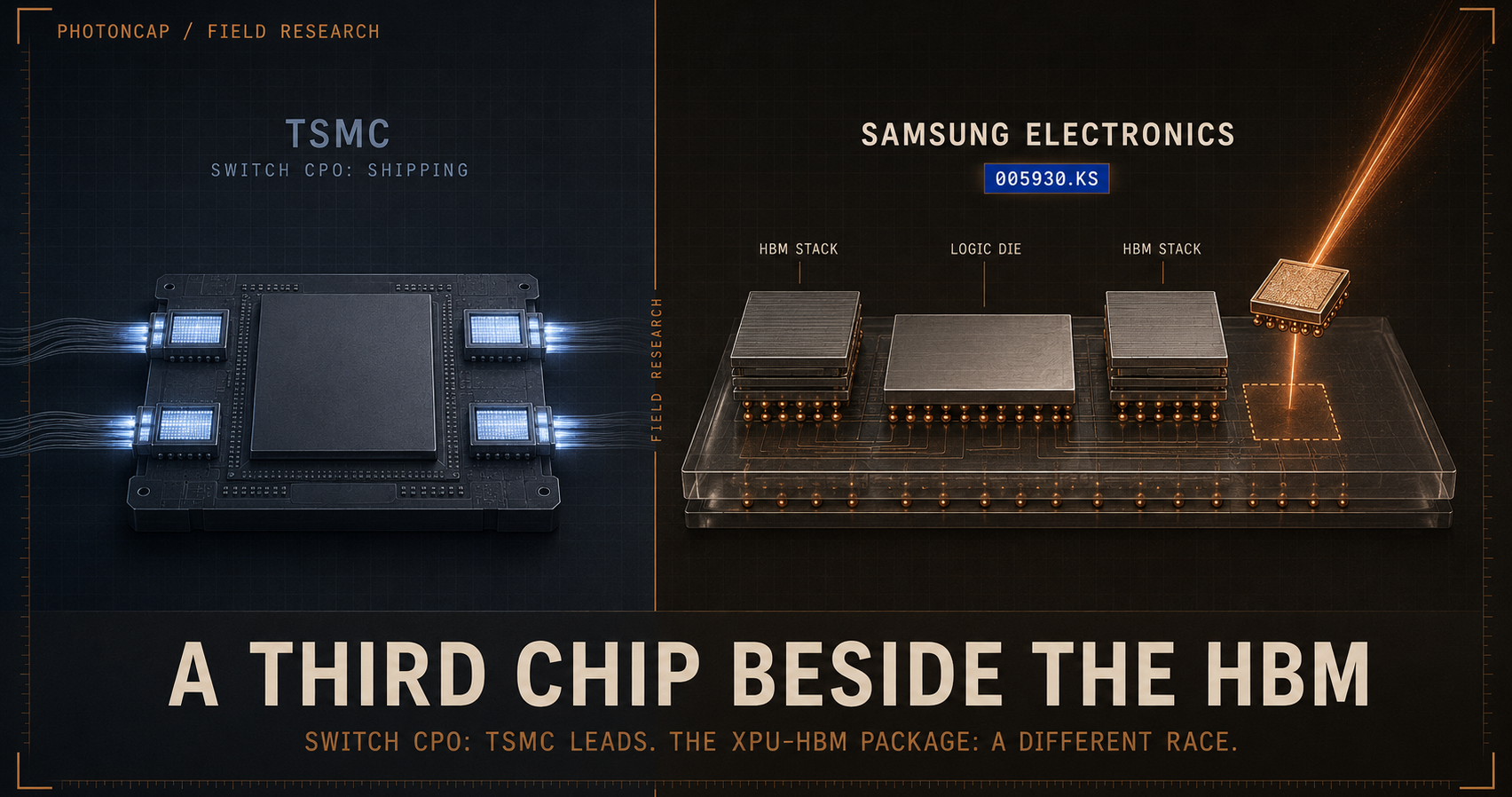
TSMC is ahead in the current CPO race. Broadcom’s 102.4 Tbps CPO switch is sampling to customers with TSMC COUPE based optical engines, and NVIDIA’s Quantum-X Photonics has started shipping. Samsung’s reported turnkey CPO roadmap points to 2029.
But that scoreboard ranks switch CPO. Once optics moves past the switch and into the package where the XPU and HBM sit, the basis of competition changes. TSMC makes logic and silicon photonics but does not make HBM itself. Samsung makes all three.
This article tests whether that difference is a real moat or an asset that has not been connected yet. We will look at the OECC 2026 speaker deck obtained on site, the first customer win, the 2.xD packaging disclosed at Nano Korea, and the multi-die yield penalty. The question is not whether Samsung can build CPO faster than TSMC. It is this: when AI’s bottleneck shifts toward memory, who can design HBM and optics together?
Contents
- Two Races: What TSMC Grabbed First, and What Hasn’t Opened Yet
- 10 to 5 to 2 pJ/bit: The Physical Reason the Race Changes
- Switch CPO and XPU-HBM Optical I/O Are Different Contests
- Three Chips: Only Samsung Makes Them All
- What the OECC 2026 Deck Shows About Samsung SiPh
- The Upside of 2.xD, and the Multi-Die Yield Penalty
- The Time Gap: TSMC Secured the First Customer References
- The Reversal Condition: When the Bottleneck Moves to Memory
- Scenarios + Monitoring
1. Two Races: What TSMC Grabbed First, and What Hasn’t Opened Yet
Let’s start with the scoreboard as it stands. TSMC has put COUPE (Compact Universal Photonic Engine) into Broadcom’s 102.4 Tbps CPO Ethernet switch, the Tomahawk 6 Davisson, which is sampling to early-access customers.[1] NVIDIA’s Quantum-X Photonics switch has started shipping, and Spectrum-X Ethernet Photonics entered production per a late-May announcement, with CoreWeave, Lambda, and Oracle Cloud Infrastructure among the first adopters (broad availability comes in the second half).[2] Both rest on TSMC’s silicon photonics and SoIC 3D stacking as their core manufacturing base.[3][4] Samsung’s turnkey CPO sits at 2029 on its reported OFC 2026 roadmap.[5][6] On the clock alone, Samsung is behind. We examined that gap, along with the wider field including Tower and GlobalFoundries, in our April piece on Samsung silicon photonics.
Then on July 9, 2026, at Nano Korea, Samsung Electronics Senior Vice President Won-Kyoung Choi pointed to a different board. He said advanced packaging that co-optimizes HBM, logic, and silicon photonics at the system level is the core of the AI era, and that Samsung is developing 2.xD, a packaging scheme that puts all three into a single package.[7] This is not today’s CPO, which pulls an optical engine next to a switch ASIC. It is the next stage: putting optical I/O into the package where the compute chip and the memory live.
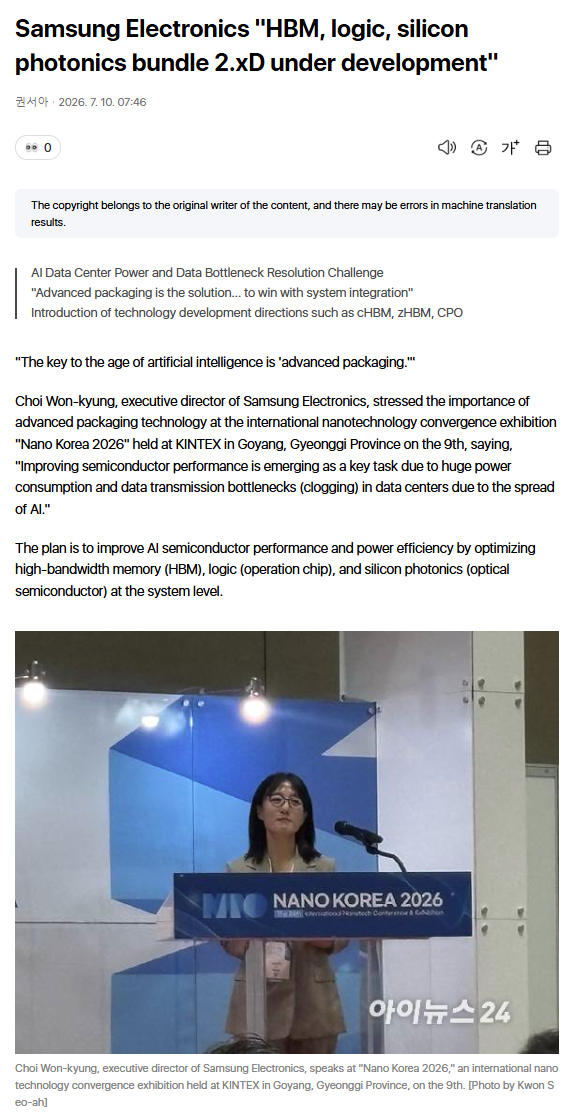
https://v.daum.net/v/20260710074609777
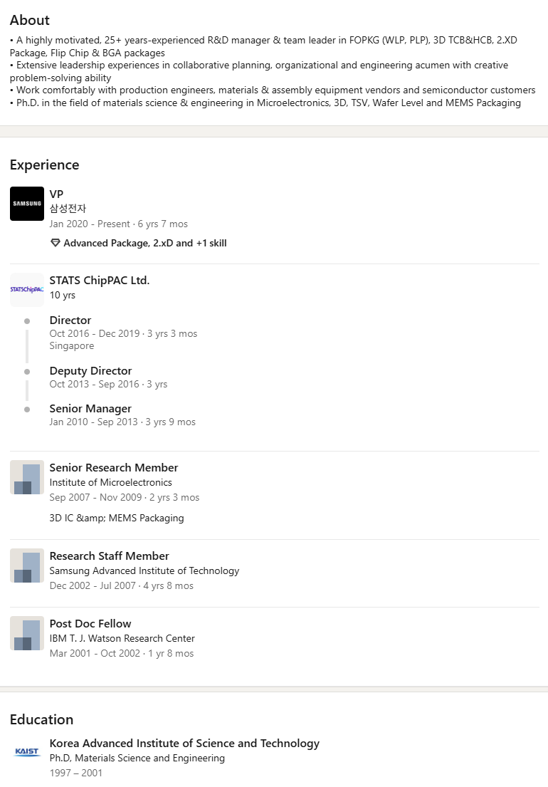
Dr. Won Kyoung Choi: https://www.linkedin.com/in/won-kyoung-choi-74775312/
TSMC has logic, silicon photonics, and CoWoS packaging, but it does not make HBM itself. Samsung makes all three. The moment optics enters the package where the XPU and HBM sit, ownership of that third chip becomes a competitive variable.
Still, owning three chips and profiting from an integrated package are separate questions. We will test this including the reason vertical integration is not an automatic moat: the multi-die yield penalty.
2. 10 to 5 to 2 pJ/bit: The Physical Reason the Race Changes
The race migrates from the switch into the package because the energy to move one bit steps down as optics gets closer to silicon. In numbers Samsung Foundry presented at OECC 2026: roughly 10 pJ per bit for pluggable optics on the board, roughly 5 pJ for an optical engine on the substrate next to the switch, and roughly 2 pJ on the interposer right beside the XPU.[8]
What makes this ladder possible is packaging. Moving the optical engine closer to the compute chip shortens the electrical path, and it cuts the signal-conditioning burden spent compensating for board and connector losses. Physics does the energy saving, but the hand that turns that physics into a product is packaging.
The physics behind the staircase is simple. Electrical signals lose more to the channel as distance grows, and beating that loss forces the transmitter and receiver to burn energy on stronger equalization and higher swing. Over distances from centimeters inside a package to a few meters between racks, fiber propagation loss changes little; coupling, optical conversion, and electronic I/O overhead dominate the link budget. So the shorter you cut the electrical leg and the sooner you convert to light, the lower the whole link’s energy budget, and the same data draws an energy staircase depending on where the optics sits.
And the ladder gets its force from the fact that data center power budgets are already at their limits. In an era when a single data center is discussed in gigawatts, the pressure to pull optics toward the package is building fast in the high-bandwidth switch tier. One caution: rather than CPO replacing every pluggable, form factors like pluggables, LPO, and CPO are likely to coexist depending on distance and power budget. NVIDIA is growing its CPO switches and its pluggable ecosystem side by side.[4] The point is not that optical modules disappear. The point is that the place where optics sits walks down the ladder, and the party executing that move changes.
Market projections point the same way. Samsung’s materials put pluggable optics (PO) at over 25% annual growth and co-packaged optics (CPO) at over 150%.[8] Read the growth-rate gap as the speed at which money is moving down the staircase.
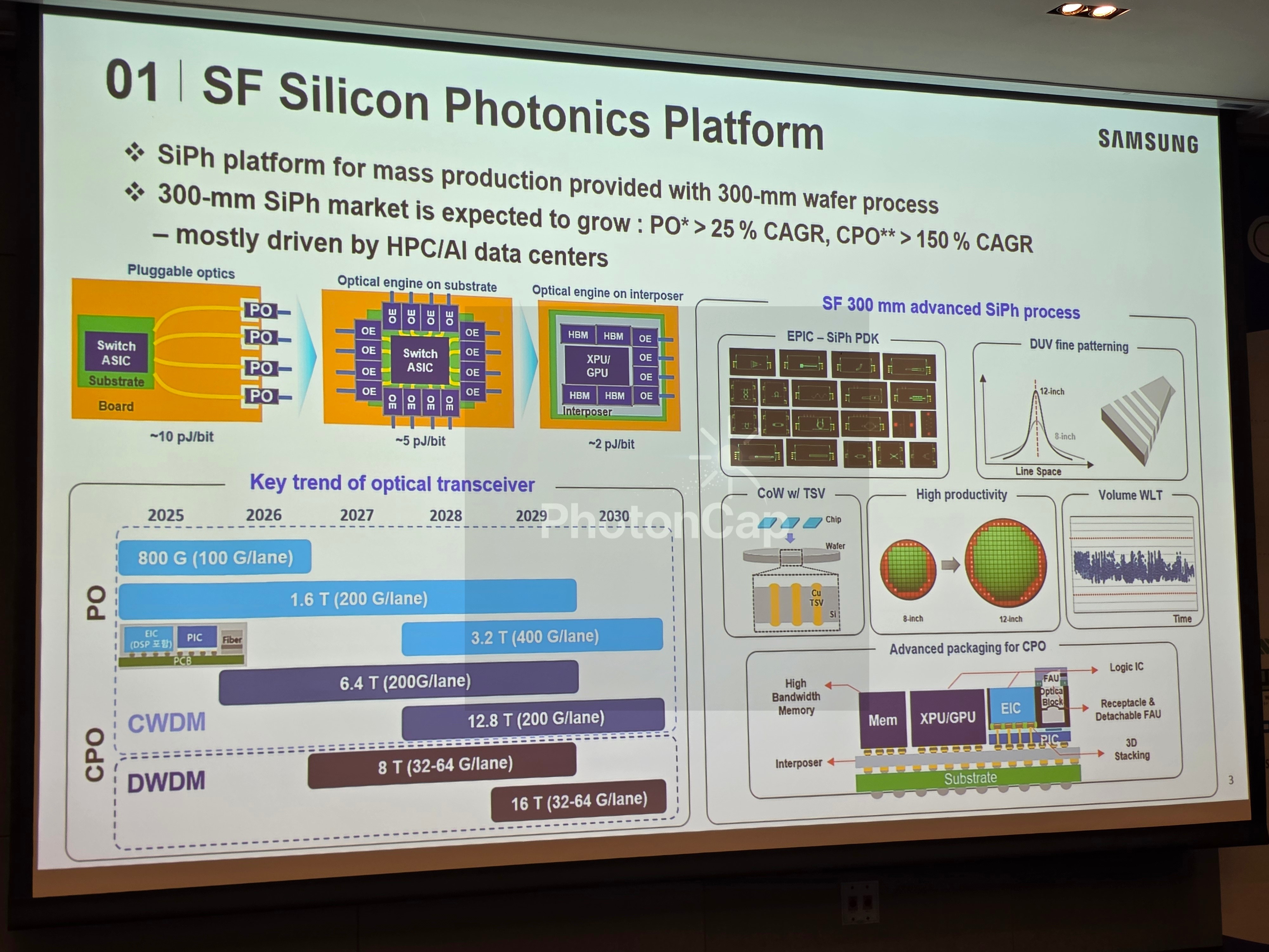
Samsung OECC 2026 slide: SiPh platform + transceiver roadmap + pJ/bit + CPO packaging overview
3. Switch CPO and XPU-HBM Optical I/O Are Different Contests
Two adjacent architectures often grouped under the CPO and optical-I/O umbrella must be kept apart.
The present: switch CPO. This pulls the optical engine next to the switch ASIC. Broadcom’s TH6-Davisson and NVIDIA’s photonics switches belong here, and HBM is not a required component.[1][3] The core capability in this contest is stacking the PIC and EIC well (bonding such as SoIC-X) and integrating them into the switch package. This is the contest TSMC leads.
The future: the XPU-HBM optical I/O package. This puts optical I/O into the package where compute and memory live. On the interposer, the XPU or GPU sits in the middle, HBM flanks it, and optical engines (PIC + EIC) sit at the edge. A logic chip, a memory chip, and an optical chip. Three kinds, sitting at one table on the interposer for the first time, and that table is exactly what this article sets out to test. 2.xD is the plan to co-optimize exactly these three in one package.[7] It extends the silicon interposer into a panel-based redistribution-layer (RDL) interposer and grows that into high-capacity system packaging for AI data centers.[7] At this stage the optical engine is no longer a switch component but a subsystem of the compute package, and the advantage goes to organizations able to co-optimize the optics and the package from the earliest design stage.
The whole foundry field is moving in this direction. TSMC is extending COUPE into CoWoS integration, and GlobalFoundries expects silicon photonics revenue of roughly $400M this year (about double last year) and targets crossing $1B on an annualized run-rate basis by the end of 2028.[9] The memory camp is moving too. SK hynix ($000660.KS) is entering this field from three directions.
- Packaging verticalization. Its $3.87B advanced packaging and R&D fab in West Lafayette, Indiana broke ground in April 2026, targeting mass production in the second half of 2028 centered on HBM4E and HBM5, with a 19-trillion-won advanced packaging fab in Cheongju in parallel.[10][11] This is a move to own HBM stacking, screening, and bonding directly.
- Reviewing CPO for the memory system. At its 2025 Future Forum, KAIST Prof. Kyoungsik Yu and SK hynix’s VP of Advanced Package Development presented “CPO technology evolution and its impact on the memory industry,” reviewing how to apply SiPh inside and around the memory system across architecture, design, device, and package.[12]
- A public CPO ecosystem. Korea’s 2026 K-CHIPS slate lists a 200 Gb/s per lambda CPO integrated design and verification platform, and the science ministry’s program runs a 6.4 Tbps opto-chiplet interposer project, with Prof. Younghyun Kim of Hanyang University as sub-project PI on both.[13][14][15] The selected participating companies are not yet disclosed.
Optics entering the package means every camp, foundry, memory, and OSAT alike, converges on packaging as the same destination. Who arrives at that point, and from which direction, draws the map of this cycle. We compared the device-level readiness of the three foundries in [OFC 2026] Part 1 of 5: 300mm SiPh Foundry: Who Is Actually Ready?, and this piece goes into Samsung alone.
That leaves the questions. Buying the three chips from three different companies and bolting them together, versus one company making all three and designing them together from the start: are those different games? If they are, how many companies make all three? And is the answer large enough to show up in Samsung Electronics’ foundry results?
That Samsung has the three axes is something we can confirm shortly. But owning three chips and selling them to a customer as one high-yield package are entirely different problems. Now let’s verify HBM, logic, and PIC one by one, weigh them against TSMC’s time advantage, and fold it all into a single twelve-month verdict at the end.
(以下为付费墙。原文第 4–9 节——三颗芯片盘点、OECC 2026 幻灯片详解、2.xD 的良率惩罚、台积电率先拿下的客户背书、反转条件、情景与监测——位于付费内容之后,本发布仅转载上述免费可读的第 1–3 节,不含任何付费内容。)
第二部分:解析(深度解读)
一、核心论点摘要
PhotonCap 这篇文章的核心是一句反问:台积电目前在「交换机 CPO」上确实领先(Broadcom TH6-Davisson 102.4T 已送样、NVIDIA Quantum-X Photonics 已出货),但 CPO 真正的胜负手不在交换机,而在「把光 I/O 放进 XPU + HBM 的同一颗封装里」。
一旦光走到 compute 与 memory 旁边,竞争基础就变了——台积电有逻辑、有硅光、有 CoWoS,但没有 HBM;三星三者都做。于是问题从「谁更快造出 CPO」变成「当 AI 瓶颈转向内存,谁能从设计之初就把 HBM 和光一起优化」。
文章用 OECC 2026 现场幻灯片、首个客户案例、Nano Korea 披露的 2.xD 封装,以及多 die 良率惩罚来验证:三星「三颗芯片都做」究竟是真实护城河,还是尚未连起来的资产。
二、关键概念解读
1. 两条容易被混为一谈的赛道
- 交换机 CPO(当下):把光引擎贴到交换机 ASIC 旁(Broadcom TH6-Davisson、NVIDIA 光交换机),HBM 非必需。核心能力是 PIC+EIC 的 3D 堆叠(SoIC-X 这类键合)并集成进交换机封装。这是台积电领先的赛道。
- XPU-HBM 光 I/O 封装(未来):把光 I/O 放进 compute 与 memory 共存的封装。interposer 上 XPU/GPU 居中、HBM 列两侧、光引擎(PIC+EIC)在边缘——逻辑、内存、光三种芯片首次同桌。优势属于「能从最早设计阶段就协同优化光与封装」的组织。
2. 10 → 5 → 2 pJ/bit 的能量阶梯
- 板级可插拔光模块 ≈ 10 pJ/bit;交换机旁基板上的光引擎 ≈ 5 pJ/bit;紧贴 XPU 的 interposer 上 ≈ 2 pJ/bit(三星 Foundry 在 OECC 2026 给的数)。
- 物理本质:电信号随距离通道损耗增大,为补偿损耗 TX/RX 要烧更多能量做均衡、加大摆幅;而光纤传播损耗在 cm~几 m 内变化很小,链路预算主要被耦合 / 光电转换 / 电 I/O 开销主导。所以越短电气走线、越早转光,整链路能耗越低。
- 驱动:单数据中心已按 GW 量级讨论,高带宽交换机层把光拉向封装的压力骤增。注意可插拔 / LPO / CPO 会按距离与功耗预算共存,而非互相取代——NVIDIA 是两边同时扩。
- 市场:三星素材给可插拔光(PO)>25% 年增、共封装光(CPO)>150% 年增;增速差即「钱下楼梯的速度」。
3. 三星的 2.xD 封装
- 把硅 interposer 延伸成 panel-based RDL interposer,再长成面向 AI 数据中心的大容量系统级封装,目标是把 HBM、逻辑、硅光三者在同一封装内协同优化。
4. 多 die 良率惩罚(反方论据)
- 拥有三颗芯片 ≠ 能高良率地作为「一个封装」卖给客户。垂直整合不是自动护城河——这是全文要验证的关键反方。
5. 内存阵营也在动(SK hynix 三路进军)
- 封装垂直化:印第安纳 West Lafayette 38.7 亿美元先进封装厂 2026/4 动工,2028 下半年量产,主攻 HBM4E/HBM5;清州 19 万亿韩元厂并行。
- 评审 CPO 对内存系统的影响:2025 Future Forum 上 KAIST 与 SK hynix 先进封装 VP 联合报告。
- 公共 CPO 生态:韩国 2026 K-CHIPS 列了 200 Gb/s/λ CPO 设计验证平台与 6.4 Tbps 光芯片 interposer 项目。
三、分层拆解表
| 维度 | 台积电 | 三星 | 关键变量 |
|---|---|---|---|
| 逻辑芯片 | 有(XPU/CPU/GPU 代工) | 有(Exynos / 代工) | 设计能力 |
| 硅光 PIC | 有(COUPE) | 有(SiPh 平台) | 良率 / 产能 |
| HBM | 无(外购 SK hynix / 三星) | 有(自产 HBM) | 内存瓶颈下的话语权 |
| 先进封装 | CoWoS / SoIC | 2.xD(规划中,2029 路线图) | 集成度 |
| 交换机 CPO 领先度 | 领先(已送样 / 出货) | 落后(2029 路线图) | 时间差 |
| XPU-HBM 光 I/O | 需外购 HBM 协同 | 三者自研可协同 | 反转条件 |
四、技术趋势与产业视角
- 赛点转移:CPO 叙事从「交换机」走向「封装内 XPU-HBM 光 I/O」,本质是 AI 算力瓶颈从 compute 移向 memory 与 interconnect。谁掌握 HBM + 光 + 逻辑的协同设计,谁就握住下一阶段门票。
- 时间差仍是硬约束:台积电已拿到 Broadcom / NVIDIA 的首批客户背书,三星 turnkey CPO 在 2029 路线图,至少在交换机 CPO 维度落后一个身位;但 2.xD 是面向「封装内三合一」的更远期形态。
- 垂直整合的悖论:三星「三颗芯片都做」是资产,但多 die 良率惩罚会让「卖成一个高良率封装」成为真正的工程门槛——这也是文章埋下的反转条件(当瓶颈转向内存时,三星的 HBM 自主权才显价值)。
- 全行业收敛到「封装」这一目的地:代工(TSMC COUPE→CoWoS、GF 硅光营收翻倍冲 10 亿)、内存(SK hynix 三路进军)、OSAT 殊途同归。
- 与本站光投资系列的连接:本站的光投资地图、CPO 百秒测试瓶颈、为何关注光测试 从「设备 / 测试 / 供应链」视角看 CPO 量产;本文补上「封装内三芯片协同」这一更上游的产业格局视角。
五、与本站其他文章的连接
- 光投资地图 v1.0 — CPO 产业链全景与卡位。
- NVIDIA CPO 背后的百秒瓶颈 — 量产瓶颈从制造转向测试,7 家设备公司卡位。
- 为什么该关注光测试 — PIC / EIC 量检测机会。
- 高速光通信入门 — 光模块与互连基础。
- 信号完整性入门 — 电气走线损耗与均衡的物理背景(对应本文 10→5→2 pJ/bit 的「电气腿越短越好」)。
六、风险提示
本文为产业研究与公开信息整理,不构成任何投资建议。三星 / 台积电的 CPO 与 HBM 路线、时间表均可能随客户订单与良率变化而调整;原文为付费专栏,本发布仅含免费可读的第 1–3 节,第 4–9 节未公开、未转载。