The 100-Second Bottleneck Behind NVIDIA CPO — CPO 测试瓶颈与四阶段测试栈
整理自 PhotonCap:CPO 量产的真正瓶颈已从制造转向测试——单颗 PIC 全检超 100 秒。拆解 4 阶段测试栈,梳理 FormFactor、Teradyne、Keysight 等 7 家公司的卡位。
The 100-Second Bottleneck Behind NVIDIA CPO: 7 Companies That Own the 4-Stage Test Stack
来源:PhotonCap (Substack) · 2026-05-08
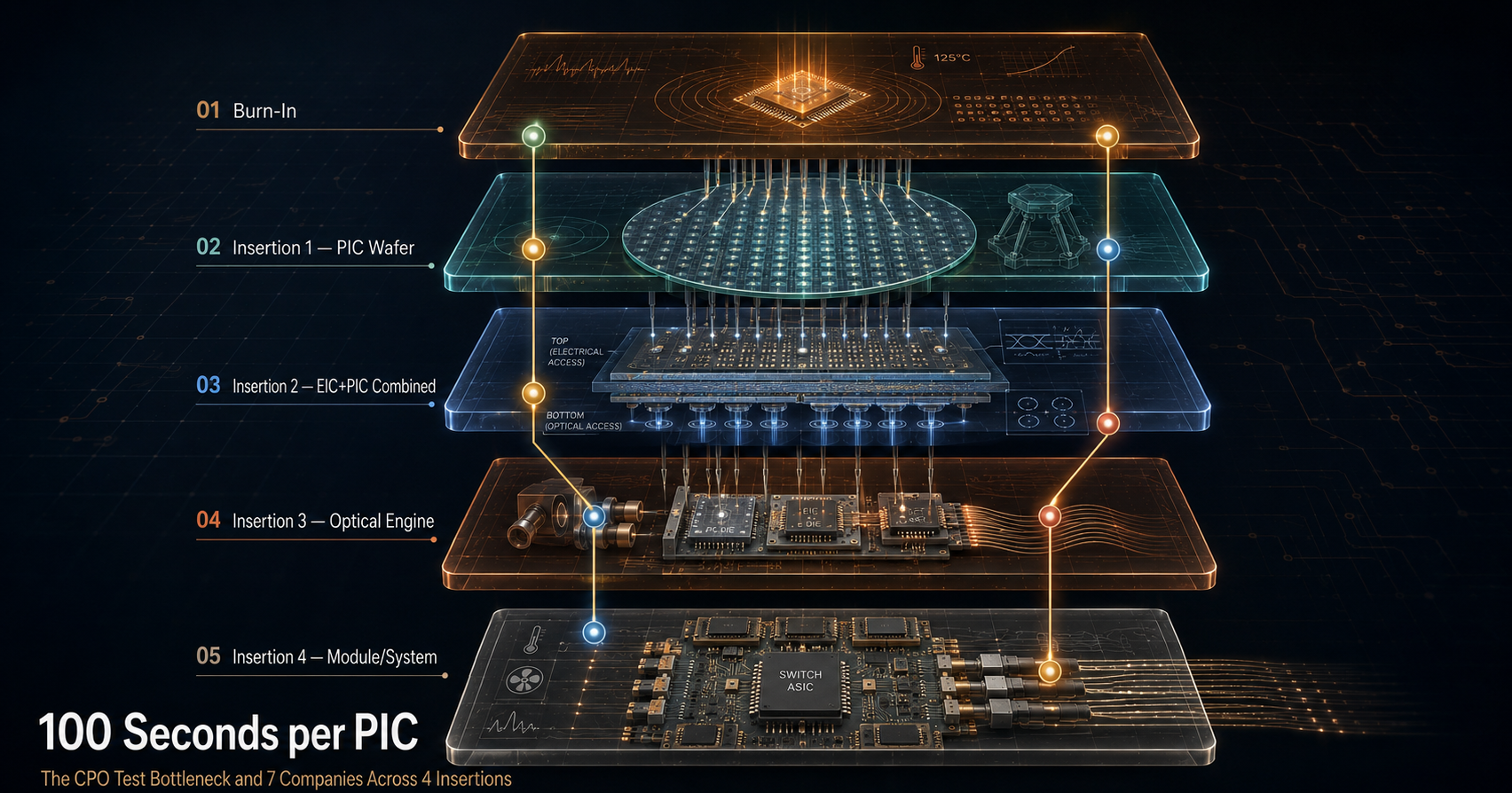
The bottleneck in CPO is no longer just “can you build the optical engine.” The bottleneck has shifted from fabrication to testing the PIC and optical engine at production speed. Per TrendForce, a full 100% optical inspection of a single CPO PIC takes over 100 seconds on average. With TSMC COUPE moving into production in 2026, the test equipment stack is emerging as a new supply chain choke point. This article breaks CPO testing into four insertions plus burn-in, and maps how FormFactor ($FORM), Teradyne ($TER), Keysight ($KEYS), Aehr ($AEHR), Advantest (6857.T), Chroma (2360.TW), and ficonTEC (private) each occupy their respective layers.
Contents
- 100 Seconds per PIC: Why CPO Test Is the Bottleneck
- Background: The Physics of Why CPO Testing Is Hard
- The 4 Insertion Framework and the Key Questions
- Insertion 1: PIC Wafer-Level Test
- Insertion 2: EIC-PIC Combined Wafer-Level Test
- Insertion 3: Optical Engine-Level Test, ficonTEC vs Chroma
- Insertion 4: Module/System-Level Test
- Burn-In: The Mandatory Step Outside the 4 Insertions
- Two Competing Axes: Bull, Gap, Optionality
- Scenario Analysis
- Monitoring Points
- Summary Table + Closing
- References & Sources
1. 100 Seconds per PIC: Why CPO Test Is the Bottleneck
Per a recent TrendForce report, a full 100% optical inspection of a single PIC (photonic integrated circuit) going into a CPO module takes over 100 seconds on average.
100 seconds. That is an order of magnitude longer than conventional semiconductor test. Over the past year, as this bottleneck became visible to the market, the equipment companies behind it moved at the opposite speed. One-year stock returns:
$AEHR +1,033%, Chroma (2360.TW) +757%, Advantest (6857.T) +389%, $FORM +468%, $TER +389%, $KEYS +150%. (as of 2026-05-06 close, price return basis, Yahoo Finance/Google Finance/Investing.com)
Market cap scales vary wildly. Advantest $128B, Keysight $62B, Teradyne $56B. These three are large-cap semiconductor equipment names. FormFactor sits at $11.6B, Aehr at $2.9B. ficonTEC is private (Germany-based, subsidiary of China’s Robo Technik). Chroma is listed in Taiwan at roughly TWD 979B (approximately $30B). Within the same CPO test ecosystem, market caps span orders of magnitude.
TSMC’s COUPE platform is entering CPO chip production in 2026. NVIDIA invested $2B in Lumentum and $2B in Coherent to secure laser and optical networking capacity. A separate $2B strategic investment in Marvell covers NVLink Fusion, custom XPU, and silicon photonics/optical interconnect. Across these three deals, $6B in AI connectivity and optics supply chain investment. Every one of these optical components needs to pass testing before it hits a production line.
Testing is becoming the single largest bottleneck in CPO mass production, and a competitive landscape is forming rapidly among equipment companies racing to solve it.
For context, consider the front-end equipment large caps. AMAT $327B, LAM $372B, KLA $236B (as of 2026-05-06). Against this group, CPO test companies sit at a distinctly different scale. Keysight ($62B), Teradyne ($56B), and Chroma (~$30B) are large test and measurement companies, but still 5 to 12 times smaller than front-end equipment leaders. FormFactor ($11.6B) and Aehr ($2.9B) are one to two orders of magnitude smaller. If CPO test grows into a multi-billion-dollar annual market comparable to front-end equipment, the market cap gap for pure-play smaller names like FormFactor and Aehr could be due for reassessment. The opposite is also possible. If CPO production gets delayed, test equipment capex gets deferred with it.
FormFactor reported Q1 2026 revenue of $226.1M (+32% YoY), beating guidance, and raised its 2026 CPO revenue guide to the high end of the $10-20M range on its earnings call. Teradyne reported Q1 2026 revenue of $1.282B (+87% YoY), with AI-related revenue accounting for roughly 70% of the total. Aehr disclosed a record $41M order from a hyperscale AI customer in April 2026 (for custom AI processor ASIC package-level burn-in). None of these data points existed a quarter ago.
Bottom line: 1Y returns for the 7 CPO test equipment companies range from +150% to +1,033%. Market caps range from $2.9B to $128B. Compared to front-end equipment large caps (AMAT/LAM/KLA at $236B to $372B), pure-play names like FormFactor ($11.6B) and Aehr ($2.9B) are one to two orders of magnitude smaller. The speed at which NVIDIA’s $6B AI connectivity investment converts to actual production volume will define the next 12 months for these companies.
2. Background: The Physics of Why CPO Testing Is Hard
Start with why it takes 100 seconds.
A single-mode fiber core has a cross-sectional area of roughly 78.5 square micrometers. A silicon photonic strip waveguide is roughly 0.099 square micrometers. That is an 800x difference. Bridging this gap requires nanometer-precision alignment to couple light in and out of the device under test. Much of this process is still partially manual. There is no unified industry standard.
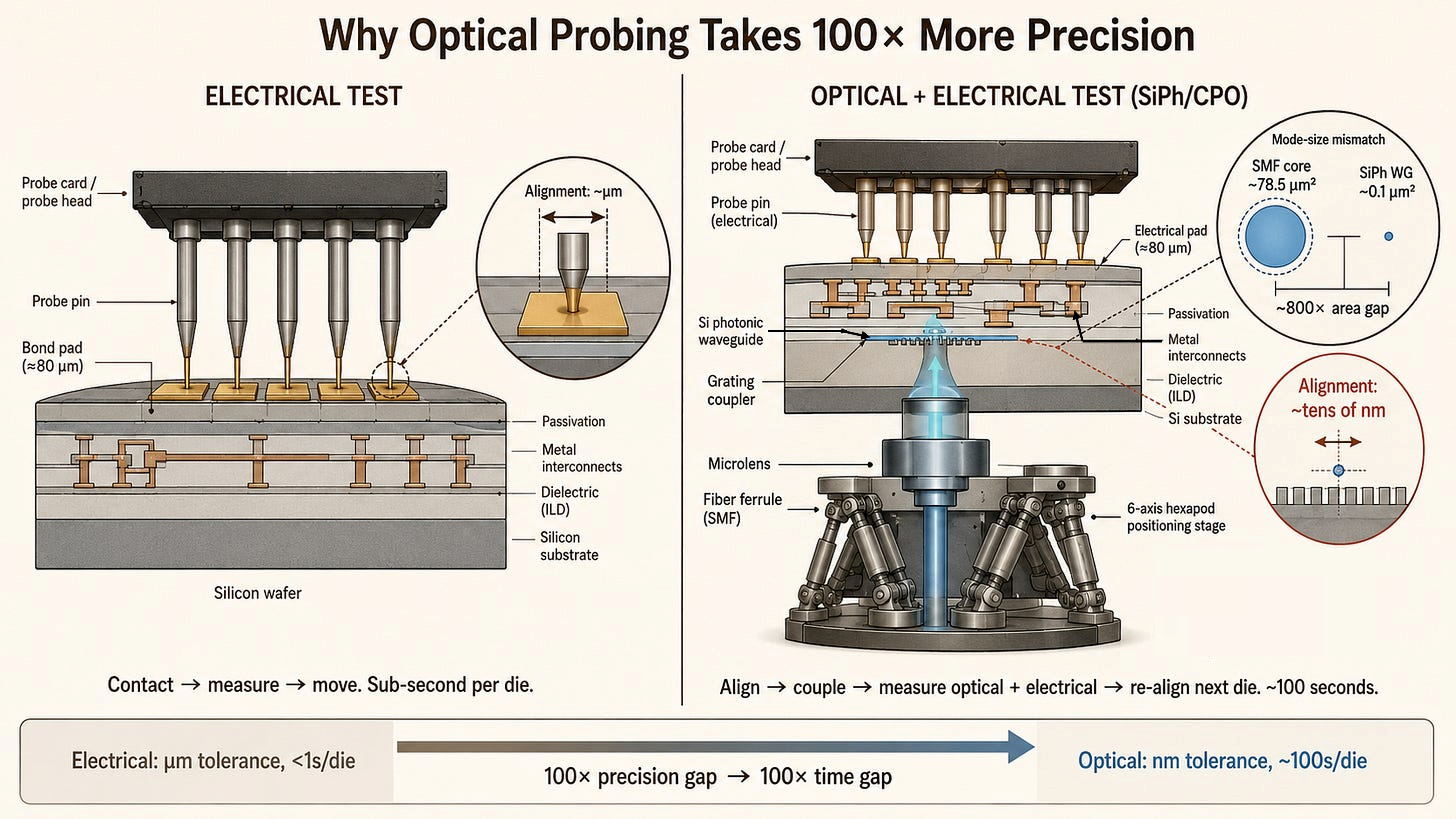 Figure 1: Electrical vs Optical Probing Comparison — 800x mode size mismatch
Conventional semiconductor test only deals with electrical signals. Touch the probe card to the pads and you are done. SiPh/CPO test requires simultaneous electrical and optical probing. You drive the modulator with electrical signals while simultaneously coupling light through an optical coupler, then receive the modulated optical signal on the output side. This requires six or more axes of precision positioning, with alignment tolerances in the tens of nanometers.
Add 3D hybrid bonding (the TSMC COUPE architecture) and it gets worse. When PIC and EIC are bonded face-to-face, the optical coupler ends up on the bottom side of the wafer. Electrical contacts are on top. You need to probe from both sides simultaneously. Existing semiconductor test equipment cannot do this.
From the perspective of established equipment companies, this is a completely different technology stack from the deposition, etch, and metrology tools that AMAT, LAM Research, and KLA ($200B to $370B market caps) dominate. In conventional wafer test, probe card pin placement accuracy at the micrometer level is sufficient. SiPh optical coupler alignment tolerance is in the tens of nanometers, roughly 100 times more stringent. Factor in thermal expansion from temperature changes (silicon CTE is roughly 2.6 ppm/K) and you cannot simply bolt an optical module onto an existing probe station. You need equipment designed from scratch for optical alignment.
There is another issue. Conventional electrical test has high repeatability. Align the probe card once and you can automatically test the entire wafer. In optical test, coupling conditions change from die to die. Waveguide position, edge coupler angle, and grating coupler pitch all carry process variation at the die level, so optical alignment must be independently optimized for each die. This accounts for a significant portion of the 100 seconds. FormFactor’s claim of sub-5-second per-die test time on the CM300xi-SiPh is a data point showing progress in alignment automation. That said, TrendForce’s “100 seconds” and FormFactor’s “sub-5 seconds” likely refer to different test content scopes. The 100 seconds appears to cover full optical inspection, while the 5 seconds likely refers to alignment plus basic parameter measurement for a specific recipe. Direct comparison requires caution.
This is why the CPO test market is being driven not by the existing equipment large caps, but by these seven companies with specialized capabilities in photonic probing, optical alignment, and burn-in.
One more piece of context. CPO test market growth is not simply proportional to CPO chip shipments. Longer test times mean more equipment is needed. Testing 1 million PICs at 100 seconds each requires 100 million seconds, roughly 27,778 equipment-hours. At 24-hour operation and 85% uptime, a single test cell processes roughly 734 PICs per day, or about 22,000 per month. 100,000 per month requires roughly 5 single-site test cells. 1 million per month requires roughly 45. Add retesting, multiple insertions, and multi-engine architectures, and actual equipment demand exceeds these figures.
The equipment competition is a test time compression competition. The company that cuts 100 seconds to 50, then to 25, can serve the same customer volume with less floor space and capex. This is why FormFactor emphasizes per-die test time reduction and ficonTEC pushes multi-site parallel testing. Throughput competition is the equipment market competition.
Bottom line: The fundamental reasons CPO test is hard are simultaneous electrical plus optical probing, nanometer alignment, and double-sided access. 100 seconds of test time per PIC directly determines how many production test cells are needed. These technical requirements open the market to specialized companies rather than the existing equipment large caps.
3. The 4 Insertion Framework and the Key Questions
CPO testing is divided into four test insertions, from wafer to system.
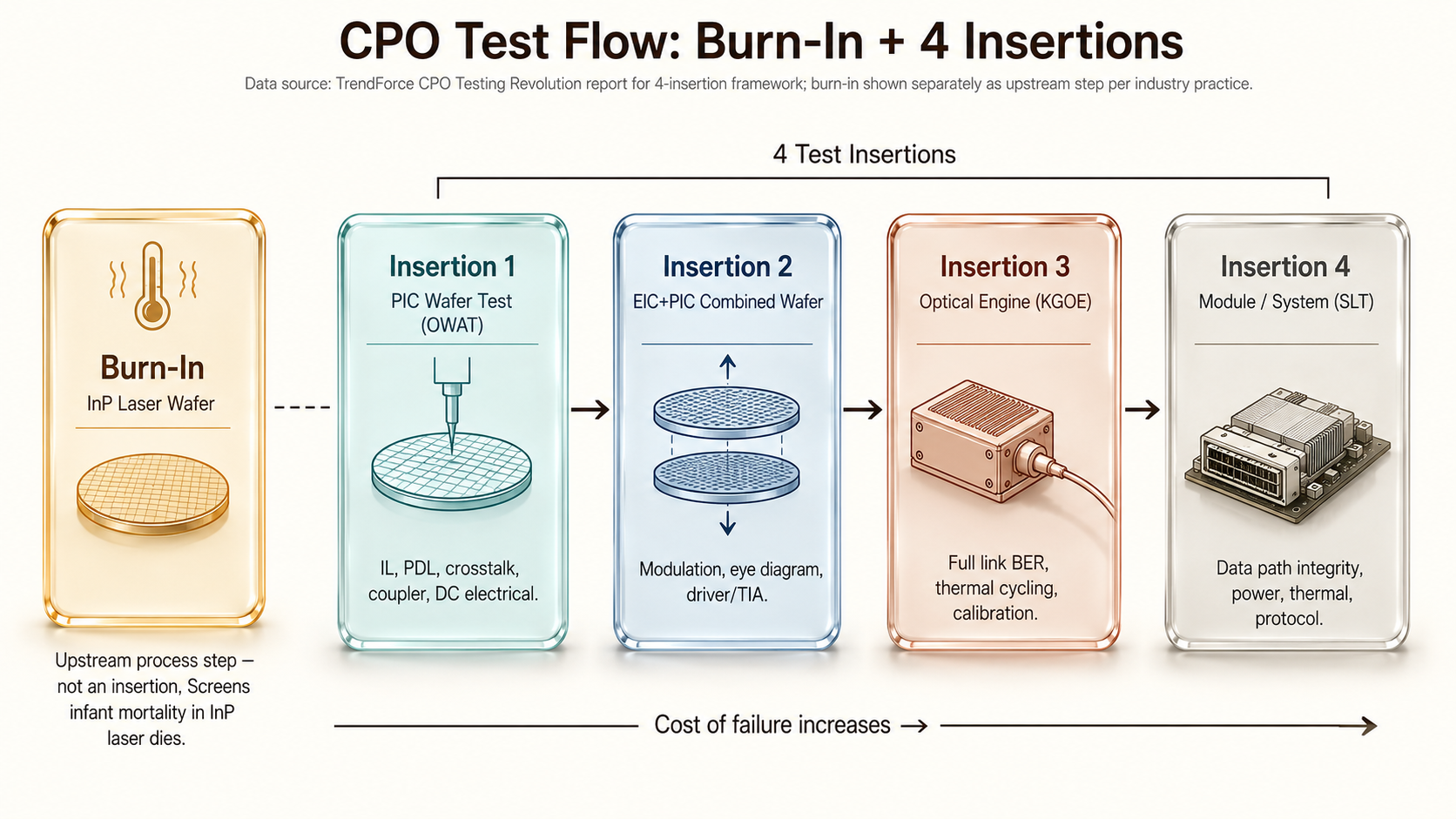 Figure 2: CPO Test Flow — Burn-In + 4 Insertions (Source: TrendForce)
Outside this four-stage framework, there is one more step. Burn-in. This is the process step that screens for infant mortality in InP lasers, performed before Insertion 1.
Everything up to this point is visible from public data and the TrendForce report. Four insertions, plus burn-in as a separate step. You can figure this out from industry conference slides and equipment company press releases.
The real differentiation starts here.
These seven companies form two distinct competing axes within the four insertion stages, with the remaining companies classified as cross-axis layer players that are not tied to either axis. The technical strengths and weaknesses of each axis are precisely inverted.
As a subscriber asked, are ficonTEC and Chroma competitors or coexisting at Insertion 3? The answer becomes clear once you understand the two-axis structure.
One more thing. One of these seven companies has a Chinese ownership structure. With CPO test becoming a choke point in production, how this structural risk could influence customer vendor selection is a critical variable.
The key questions the paid section addresses:
- How each axis’s technical strength can flip into a weakness under specific conditions
- Why cross-axis layer players remain relatively stable regardless of scenario
- Whether the order-of-magnitude differences in market cap among these seven companies reflect their actual positioning in the CPO test market, or whether the market is still mispricing them
One preview: the most interesting point of competition between the two axes is not technology. It is corporate structure. How one axis’s key partner’s ownership structure could distort customer vendor selection may be the most underpriced variable in the investment equation. Especially in the current environment where US-China technology competition is extending into the semiconductor equipment supply chain.
⚠️ 以上为公开免费部分。第 4–13 节(各 Insertion 详解、Burn-In、双轴竞争格局、情景分析、监测点、汇总表、参考文献)为付费内容,未包含。
第二部分:深度解析
文章核心论点摘要
- 瓶颈转移:共封装光学(CPO)技术量产的瓶颈,已从”如何制造光学引擎”转移到”如何以量产速度测试光学引擎”。单个光子集成电路(PIC)的全面光学检测耗时超过100秒,是传统半导体测试的10倍以上。
- 测试设备成为新咽喉:随着台积电COUPE平台在2026年进入量产,以及英伟达在光学互联领域60亿美元的布局,CPO测试设备供应链正成为新的关键瓶颈。解决测试速度和精度问题的专业设备公司,将获得巨大增长机会。
- 竞争格局初现:围绕CPO测试的四个关键环节(晶圆级、芯片级、引擎级、模块级)及老化测试,形成了以FormFactor、Teradyne、Keysight、Aehr、Advantest、Chroma和ficonTEC为代表的七家公司竞争格局。这些公司的市值从30亿美元到1280亿美元不等,存在巨大的价值重估空间。
关键概念解读
- CPO (共封装光学):将光学引擎(负责光信号收发)和电芯片(负责数据处理)封装在一起,缩短两者间的距离,以解决传统可插拔光模块在高速数据传输时功耗高、信号损耗大的问题。可以理解为把”光猫”直接集成到”路由器”芯片旁边。
- PIC (光子集成电路):光路版的”芯片”,负责处理光信号,如调制、解调、路由等。它由波导、调制器、探测器等光学元件集成在硅基或磷化铟衬底上。
- EIC (电子集成电路):负责驱动和控制PIC的电子芯片,通常是CMOS工艺。在CPO中,EIC和PIC通过3D混合键合等技术紧密贴合。
- KGD (已知良好芯片):在封装前,确保每个芯片(无论是PIC还是EIC)都是功能完好的。这是提高最终封装良率的关键步骤,也是CPO测试的核心挑战之一。
- WLBI (晶圆级老化测试):在晶圆切割前,对整个晶圆上的芯片进行高温、高压下的加速老化测试,以筛选出早期失效的芯片。这是确保激光器等组件可靠性的关键步骤。
- COUPE (紧凑型通用光子引擎):台积电推出的先进CPO封装平台,采用3D混合键合技术将PIC和EIC面对面贴合,实现了更高的集成度和性能。
- ATE (自动测试设备):用于自动化测试半导体芯片功能和参数的设备。在CPO领域,ATE需要同时处理电信号和光信号。
- Burn-in (老化测试):一种可靠性筛选测试,通过施加高温、高电压等应力,让芯片在短时间内经历相当于数月甚至数年的使用环境,从而剔除那些有”早期夭折”风险的芯片。
“100秒瓶颈”的物理根源
为什么CPO测试这么难?核心在于”光”和”电”的物理本质差异:
- 巨大的尺寸鸿沟:单模光纤的纤芯直径约10微米,而硅光波导的截面尺寸仅约0.1微米。两者相差800倍。要将光高效地耦合进/出PIC,需要纳米级的对准精度,这比传统电测试的微米级对准要求严格100倍。
- 光-电并行测试:传统芯片测试只需电探针接触焊盘即可。CPO测试必须同时进行电信号驱动和光信号耦合。测试系统需要驱动调制器(电),同时通过光纤精确对准光耦合器(光),再接收并分析输出的光信号。这需要6轴或更多维度的精密运动控制。
- 双面探测难题:以台积电COUPE为代表的3D架构,PIC和EIC面对面键合后,光耦合器位于晶圆底部,电触点位于顶部。现有测试设备无法同时从上下两面进行探测,需要全新的设备设计。
- 逐芯片对准:传统电测试,探针卡一次对准即可测试整个晶圆。而光学测试中,由于工艺偏差,每个芯片的波导位置、耦合器角度都不同,必须为每个芯片独立优化光学对准。这消耗了大量时间,是”100秒”的主要来源。
4阶段测试插入框架逐一解读
| 测试阶段 | 测试内容 | 难点 | 卡位公司 |
|---|---|---|---|
| 插入1:PIC晶圆级测试 | 在PIC晶圆上,对单个PIC进行光学和电学参数测试,筛选出KGD。 | 需要同时进行高速电探针和纳米级精度的光纤对准。测试时间长,是”100秒瓶颈”的核心环节。 | FormFactor (CM300xi-SiPh探针台) |
| 插入2:EIC-PIC组合晶圆级测试 | 在EIC和PIC通过3D键合后,对组合体进行测试。 | 需要从晶圆背面(PIC侧)进行光学耦合,同时从正面(EIC侧)进行电探测。设备需支持双面访问。 | Teradyne (与FormFactor合作开发) |
| 插入3:光学引擎级测试 | 将切割后的PIC-EIC组合体(光学引擎)进行最终功能测试。 | 高速、高精度、多通道并行测试。需要处理大量光纤阵列的自动对准。 | ficonTEC (高精度对准) vs. Chroma (多站点并行) |
| 插入4:模块/系统级测试 | 将光学引擎与激光器、驱动芯片等组装成完整CPO模块后,进行系统级功能和性能测试。 | 测试复杂度高,需要模拟真实网络环境,测试误码率、功耗等系统级指标。 | Keysight (高速数字/光通信测试仪) |
| 老化测试 (Burn-in) | 在插入1之前,对激光器晶圆进行WLBI,筛选早期失效。 | 需要能同时处理大量激光器的高温、高压老化系统。 | Aehr (晶圆级老化测试系统) |
7家公司竞争格局分层分析
| 层级 | 公司 | 市值 (约) | 纯度/卡位 | 核心优势与风险 |
|---|---|---|---|---|
| 大型综合设备商 | Advantest (6857.T) | $128B | 低纯度,传统ATE巨头 | 在CPO测试领域布局较晚,但凭借强大的客户关系和系统集成能力,可能在模块级测试占据一席之地。 |
| Keysight ($KEYS) | $62B | 中纯度,光通信测试龙头 | 在高速数字和光通信测试领域拥有无可比拟的技术优势,是模块/系统级测试的天然领导者。 | |
| Teradyne ($TER) | $56B | 中纯度,SoC测试龙头 | 与FormFactor合作,卡位插入2的组合晶圆级测试。其强大的电测试平台是优势,但光学部分依赖合作伙伴。 | |
| 高纯度/高弹性公司 | Chroma (2360.TW) | ~$30B | 高纯度,自动化测试方案商 | 在插入3的光学引擎级测试中,主推多站点并行测试方案,直接挑战ficonTEC。其台湾背景在供应链安全上具有优势。 |
| FormFactor ($FORM) | $11.6B | 极高纯度,PIC探针台龙头 | 直接解决”100秒瓶颈”的核心公司。其CM300xi-SiPh探针台是插入1的标杆产品。市值相对前三大公司有巨大增长空间。 | |
| Aehr ($AEHR) | $2.9B | 极高纯度,WLBI专家 | 在激光器老化测试领域拥有独特技术,是CPO量产不可或缺的一环。市值最小,弹性最大,但业务单一,风险也最高。 | |
| 私营公司 | ficonTEC (私有) | 未上市 | 极高纯度,高精度对准专家 | 在插入3的光学引擎测试中,以超高精度和灵活性著称。但其德国背景及中国母公司股权结构,可能在地缘政治背景下影响客户选择。 |
投资逻辑:为什么测试设备是CPO量产的真正瓶颈?
- 测试时间决定产能:100秒/PIC的测试时间,意味着每台测试设备每月只能处理约22,000个PIC。要实现百万级月产量,需要45台以上的测试设备。测试设备的需求量直接与CPO出货量挂钩,且由于测试时间长,设备需求弹性远大于传统芯片。
- 技术壁垒高:CPO测试需要同时解决纳米级光学对准、高速电信号、双面探测等跨学科难题,传统半导体设备巨头(如AMAT、LAM)难以直接切入。这为FormFactor、Aehr等专业公司创造了”蓝海”市场。
- 价值量提升:在传统芯片制造中,测试设备成本占比相对固定。但在CPO中,由于测试难度和时长剧增,测试设备在总资本支出中的占比将显著提升,为相关设备公司带来更大的市场空间。
- “卖铲子”逻辑:无论最终哪家公司的CPO方案胜出(英伟达、博通、Marvell等),都需要经过这4个测试环节。投资测试设备公司,本质上是投资整个CPO产业链的”卖铲子”生意,风险相对分散。
关键时间节点和催化剂
- 2026年:台积电COUPE平台进入量产。这是CPO从研发走向规模量产的关键转折点,将直接拉动对测试设备的需求。
- 英伟达60亿美元投资落地:英伟达对Lumentum、Coherent、Marvell的投资,将转化为对光模块和光学引擎的采购订单,进而转化为对测试设备的需求。
- 季度财报:FormFactor、Teradyne、Aehr等公司的季度财报中,关于CPO相关收入的指引和订单数据,是验证投资逻辑是否兑现的关键信号。
- 技术突破:哪家公司能将单PIC测试时间从100秒压缩到50秒甚至更低,将获得巨大的竞争优势,其股价可能迎来爆发。
风险提示
- 技术路径风险:CPO技术仍在快速演进,可能出现新的封装形式或测试方法,导致现有设备方案被淘汰。
- 量产延迟风险:CPO的量产良率和成本可能不及预期,导致大规模部署推迟,测试设备资本开支相应延后。
- 竞争加剧风险:传统ATE巨头(如Advantest)可能通过收购或自研快速切入,加剧市场竞争,压缩专业公司的利润空间。
- 地缘政治风险:中美科技竞争可能影响供应链安全。例如,ficonTEC的中国背景可能使其失去美国客户的订单,而Chroma的台湾背景则可能成为其优势。
- 估值风险:部分公司(如Aehr)股价在一年内上涨超过10倍,已充分反映了乐观预期。一旦CPO量产进度不及预期,股价可能面临大幅回调。
- 客户集中度风险:目前CPO市场高度集中于少数几家大客户(如英伟达、谷歌、微软等),设备公司的收入高度依赖这些客户的资本开支计划。