Everything You Need to Know About CPO Testing — CPO 你需要知道的一切
整理自 Damnang(Substack)的英文原文 Everything You Need to Know About CPO Testing,并附中文深度解读,系统拆解 CPO 测试的价值链、技术难点与投资含义。
本文整理自 Damnang(Substack)(damnang2.substack.com),原文发布于 Apr 07, 2026(标题原文:Everything You Need to Know About CPO Testing)。 结构为 正文(英文原文)+ 解析(中文深度解读),方便中英对照阅读。 来源说明:内容经公开页面获取;本发布保留完整英文原文并附中文深度解读,仅作信息整理与学习用途,著作权归原作者所有,建议在原站支持作者订阅。 ⚠️ 本文含付费段落,以下仅发布公开可读部分;付费深解(分阶段测试设备清单与厂商格局)未包含。
第一部分:正文(Original Article)
Everything You Need to Know About CPO Testing
Damnang · Apr 07, 2026
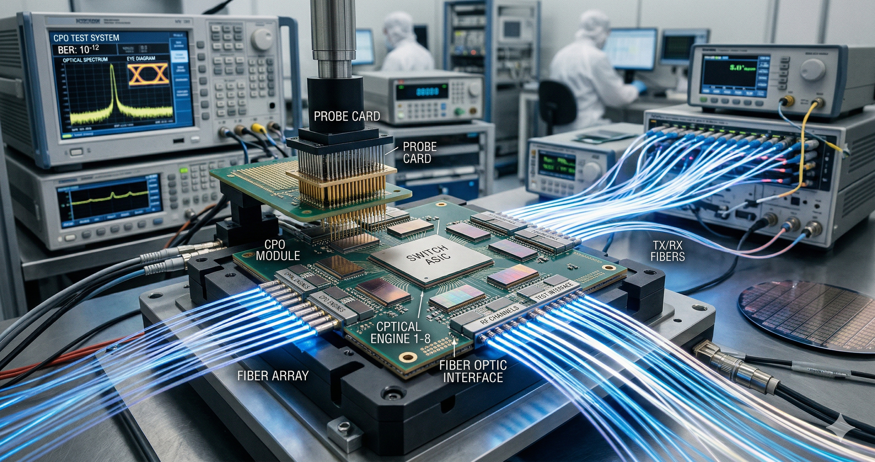
Interest in CPO (Co-Packaged Optics) is exploding.
Broadcom is in volume production with its second-generation CPO based on Tomahawk 5, and NVIDIA announced at GTC 2026 that the Quantum-X photonic switch has entered full production.
TSMC is moving its COUPE platform into volume production this year, and Samsung Foundry has announced a CPO turnkey target for 2029.
As bandwidth bottlenecks in AI data centers collide with the physical limits of copper interconnects, CPO is no longer a technology of the future. It’s a production reality, integrating optics directly into ASIC packages.
But there’s one area most investors and engineers overlook: CPO testing.
Building CPO is hard enough. Testing it is a different problem entirely. Conventional ASICs are tested with electrical signals alone. CPO requires measuring electrical and optical signals simultaneously, at sub-micron precision. That’s precisely why the semiconductor test infrastructure that took 50 years to optimize is getting rewritten from scratch.
The Real Bottleneck in the Optical Era: Test and Yield
If you’ve been evaluating CPO investments by looking only at lasers, optical engines, and packaging, there’s a good chance you’ve been missing the most undervalued segment in the value chain.
This article covers why CPO testing represents an opportunity going forward, walks through the full CPO test process stage by stage, and examines which companies deserve attention at each step. If your knowledge of CPO testing has been fragmented, this article will connect the full picture.
Disclaimer
This article is a technical analysis based on publicly available information and general industry knowledge. It contains no NDA-protected or confidential information related to the author’s current employer. Nothing here constitutes a buy or sell recommendation. All investment decisions are the reader’s own responsibility.
Damnang2’s Substack is a reader-supported publication. To receive new posts and support my work, consider becoming a free or paid subscriber.
How Conventional ASIC Testing Works
Here’s the semiconductor test flow. Once a chip is finished, it goes through three major stages.
🔗 延伸阅读:How Do We Actually Test Semiconductors?(Mar 21)
First, Wafer Sort. In wafer state, probe card needles contact each die’s pads. Electrical signals go in, electrical signals come out. From open/short tests to functional tests, the ATE (Automatic Test Equipment) handles everything. Defective dies get marked with ink or flagged in a map.
Second, Package Test. After dicing and packaging, the chip goes back on the ATE. Handlers pick chips and load them into sockets, and the tester verifies all functions via electrical signals. Temperature conditions are applied too: high temp, low temp, ambient. Speed binning happens here as well.
Third, System Level Test (SLT). The chip runs in conditions that approximate a real system environment. Does it boot? Can it process actual workloads?
All three stages share one thing: they’re entirely electrical.
Probes contact pads, signals go in, signals come out. It’s the paradigm that has been optimized for over 50 years, and every ATE platform, probe card, handler, and socket in the industry was built on this assumption.
But as copper interconnects hit their limits in AI data centers, optical interconnects that transmit data using light have entered the picture. Optical signals are now intruding on test infrastructure that was designed to handle only electrical ones. To understand what this shift means, you first need to understand what an optical module actually is.
Optical Modules: PIC and EIC
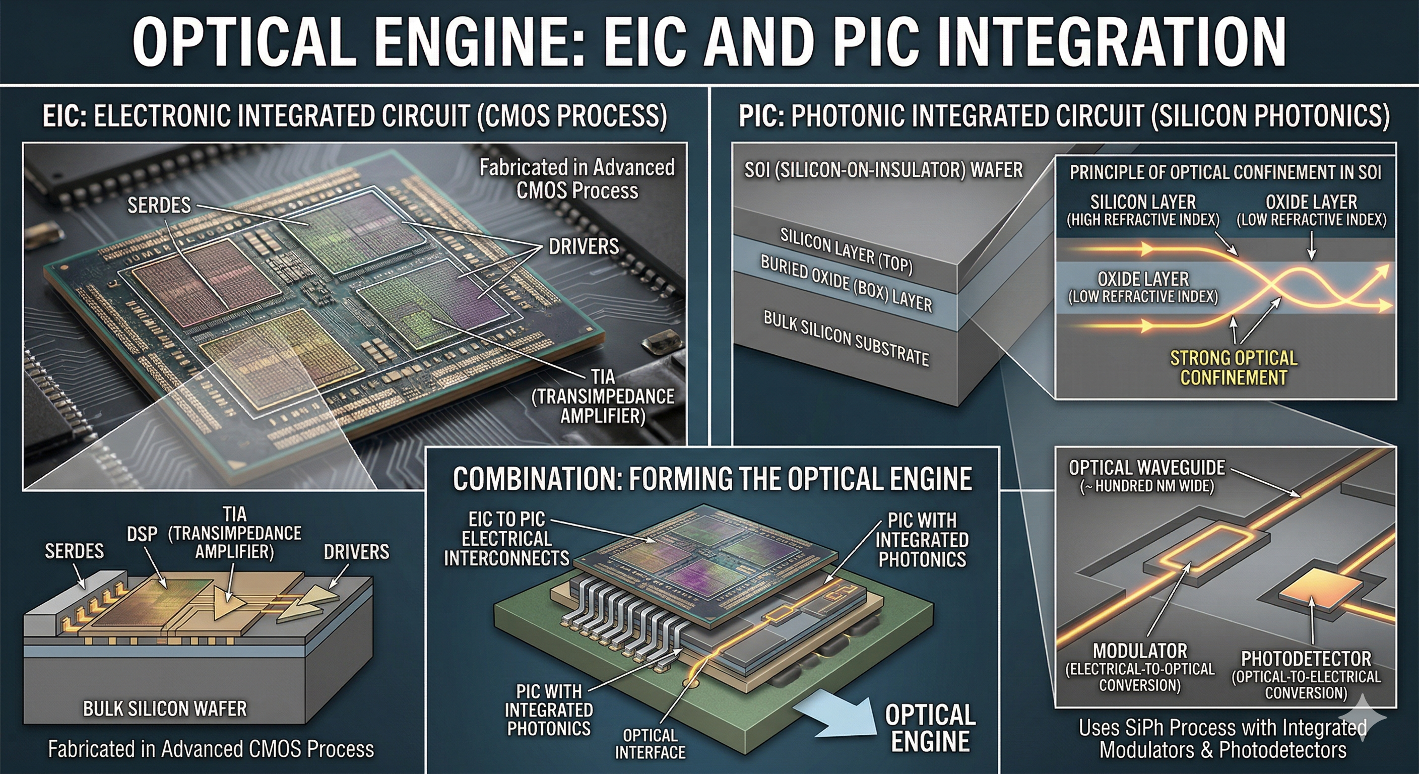
Transmitting data between chips in a data center using light instead of copper requires opto-electronic conversion. That function is handled by optical modules. Inside an optical module sits an optical engine, or an equivalent opto-electronic conversion block. This article focuses on silicon photonics (SiPh)-based optical engines. A SiPh-based optical engine typically consists of a PIC (Photonic IC) and the EIC (Electronic IC) that drives it.
🔗 延伸阅读:CPO Fully Dissected (CPO Special Part)(Mar 19)
The EIC is close to what we think of as conventional semiconductor logic. It contains circuit blocks like SerDes, DSP, TIA (Transimpedance Amplifier, a circuit that amplifies the weak current from a photodetector), and drivers, fabricated in an advanced CMOS process.
The PIC is different. PICs are made using Silicon Photonics (SiPh) processes. Conventional semiconductors use bulk silicon wafers, but SiPh uses SOI (Silicon-on-Insulator) wafers. An SOI wafer has a layer of oxide (BOX, Buried Oxide) beneath the silicon layer.
The BOX layer’s refractive index is far lower than silicon’s, and this low-index layer creates strong optical confinement within the silicon layer. Using this principle, optical waveguides just a few hundred nanometers wide can be etched into the silicon layer, with modulators (devices that convert electrical signals into optical signals) and photodetectors (devices that convert optical signals back into electrical signals) integrated on top. The finished result is a PIC.
One note: silicon itself is not a favorable material for laser emission, so real-world optical engines require a separate laser source, either an external laser source module or a III-V compound semiconductor for light generation. This article covers the PIC/EIC-centered test flow; laser source testing is a separate topic and is not addressed here. For more details on lasers, please refer to the article below
🔗 延伸阅读:The War of Light: A Laser Shortage(Mar 31)
The combination of EIC and PIC is the optical engine. Pluggable, NPO, and CPO all require opto-electronic conversion. The difference lies in how closely that conversion block is placed relative to the ASIC.
How the Optical Module Attaches: Pluggable, NPO, CPO
There are three configurations based on how closely the optical engine is integrated with the ASIC.
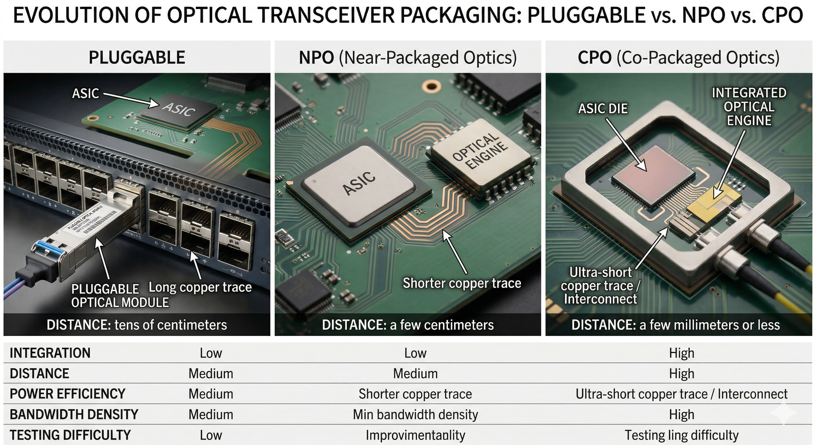
Pluggable means optical transceiver modules plug into cages on the front panel of a switch. The ASIC and module sit roughly tens of centimeters apart.
NPO (Near-Packaged Optics) is a middle-ground architecture that places the optical engine immediately adjacent to the ASIC, closing the gap to roughly a few centimeters.
CPO (Co-Packaged Optics) integrates the optical engine or optical subassembly into the same package as the ASIC, with separation on the order of a few millimeters or less. The closer the integration, the shorter the copper traces, which improves power efficiency and bandwidth density. But testing gets dramatically harder.
Here’s how each looks from a test perspective.
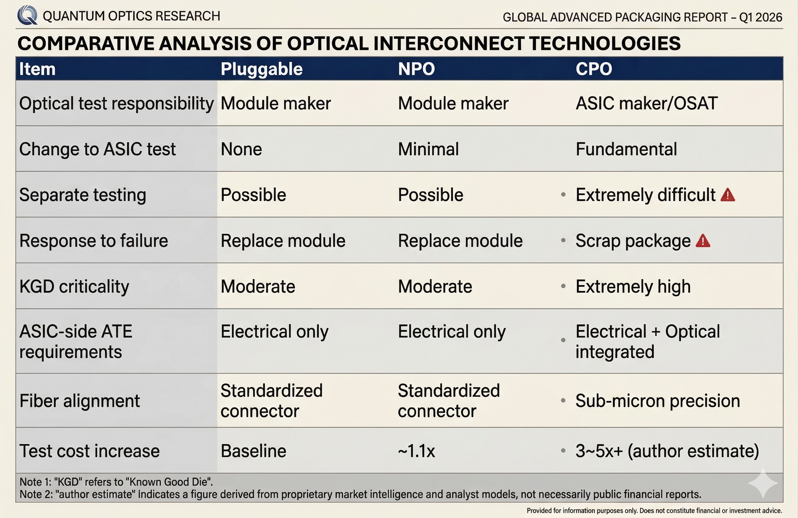
Pluggable modules are the most familiar form. Standardized transceiver modules like QSFP-DD or OSFP plug into the front panel of a switch. The ASIC and optical engine are physically separate. The biggest testing advantage is that each can be tested independently. The ASIC follows the conventional ATE flow on its own. The optical module is tested by the module maker independently. You secure a KGD (Known Good Die) and a Known Good Module separately, then assemble. If something fails, you pull the module and replace it.
NPO (Near-Packaged Optics) is a middle-ground architecture that places the optical engine directly adjacent to the ASIC. Implementations vary by vendor: some mount components on the same board in close proximity, others integrate them on a shared substrate near the ASIC package. Shorter copper traces improve signal integrity. Compared to CPO, the ASIC and optical engine are still physically separate, so independent testing and replacement remain possible. That said, differences in proximity, fiber routing, and thermal conditions mean system integration testing isn’t identical to pluggable.
CPO is a different dimension entirely. The optical engine or optical subassembly is integrated with the ASIC in the same package or first-level substrate. In NVIDIA’s Quantum-X, TSMC COUPE-based optical subassemblies are co-integrated with the switch ASIC in a single package. Total throughput: 115.2 Tbps, 144 ports at 800G.
With CPO, pulling a module and swapping it the way you would with pluggable is extremely difficult once the assembly is complete. If there’s a defect in the PIC, rework is enormously burdensome, and in practice you’re often looking at scrapping the entire high-value package.
Why CPO Testing Is So Hard
In CPO, securing a Known Good Die for the PIC before co-packaging is what makes or breaks volume production. The catch: fully verifying a PIC’s optical characteristics at the wafer level is hard. Some defects only reveal themselves after packaging. And the verification process itself is fundamentally different from conventional semiconductor testing.
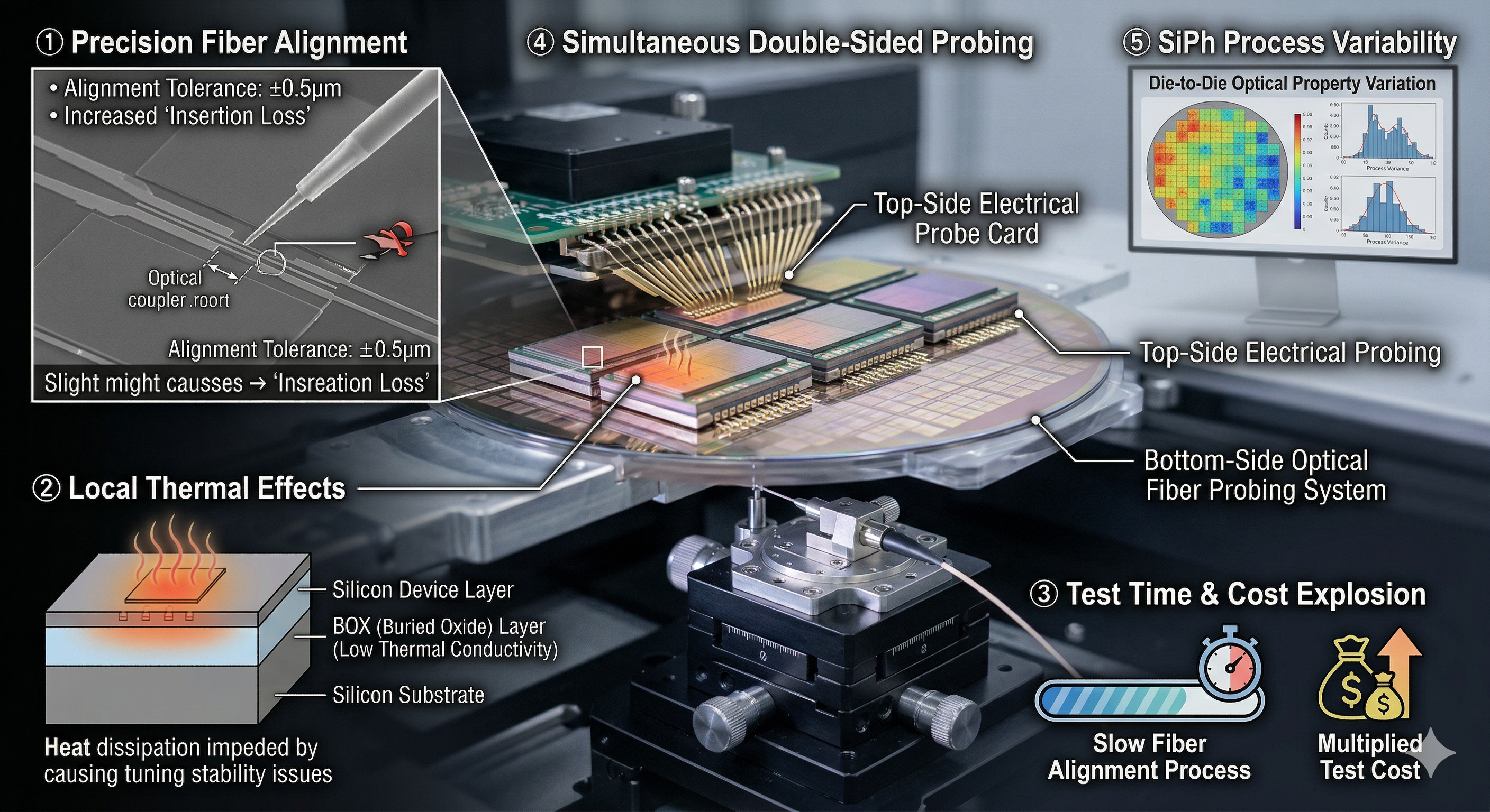
Fiber alignment. To test a PIC, you need to bring an optical fiber precisely to the coupler on the chip, the port that routes light in and out of the die. This is a completely different scale from the tens-of-microns precision of conventional electrical probe cards. Alignment tolerance varies from sub-micron to a few microns depending on the coupler structure, and even small misalignments can cause a significant jump in insertion loss. The accuracy of optical measurements is directly tied to alignment quality.
Thermal effects. Laser source wavelength is temperature-sensitive. The ring modulators inside a PIC shift their resonance wavelength with temperature changes. The SOI wafer’s BOX layer has roughly 100 times lower thermal conductivity than silicon, which impedes heat dissipation and can cause local thermal non-uniformity and tuning stability problems. In conventional ASIC testing, applying temperature conditions was about verifying device operating specs. In CPO, temperature control becomes far more critical and thermal stability is much harder to manage. The BOX layer’s low thermal conductivity can actually benefit thermal tuning efficiency in some respects, but in a test environment it makes maintaining uniform temperature significantly more difficult.
Test cost explosion. Aligning a fiber to a coupler takes time. Even with automated equipment, it’s incomparably slower than electrical probing. Add simultaneous electrical testing on top, and the fully loaded per-chip test cost, including equipment depreciation, test time, and consumables, multiplies several times over.
Double-sided probing. For wafers where EIC and PIC have been stacked via hybrid bonding, you need to probe electrical pads from the top while presenting optical fiber to the coupler from the bottom. Accessing both sides of the wafer simultaneously is something conventional prober infrastructure was never built to handle.
SiPh variability. Because SiPh process variability is high, PIC wafers show large die-to-die and wafer-to-wafer variation in optical characteristics. There is still no industry standard for test guardband optimization.
Simultaneous electrical and optical measurement, sub-micron precision, double-sided probing, active thermal management, high process variability. Conventional ATE infrastructure can’t handle it. So what stages does CPO testing actually go through, what equipment is needed at each stage, and among the companies building that equipment, who is best positioned?
第二部分:解析(深度解读)
一、这篇文章为什么重要
过去两年,CPO(Co-Packaged Optics,共封装光学)的叙事一直集中在「谁来做光引擎、谁来做激光器、谁来做封装」这三条线上——Broadcom 的 Tomahawk 5 二代 CPO 已量产、NVIDIA 在 GTC 2026 宣布 Quantum-X 光子交换机进入全量产、TSMC 的 COUPE 平台今年转入量产、Samsung Foundry 把 CPO turnkey 目标定在 2029。换句话说,”CPO 能不能做出来”已经不是问题,”CPO 能不能大规模、高良率地测出来”才是。
这篇文章的独特价值,在于它把视角从「器件与集成」转向了半导体价值链里最被忽视、却最可能决定量产爬坡速度的环节——测试(Test)与良率(Yield)。作者开宗明义地指出:CPO 测试是”被低估的环节(most undervalued segment)”。对一个关注半导体设备的投资者而言,这是一个典型的”共识还没定价、但产业瓶颈已经显现”的切入点——正如作者此前《The Real Bottleneck in the Optical Era: Test and Yield》一文所铺垫的逻辑。
为什么测试会突然变成瓶颈?因为过去 50 年优化的整套 ATE(自动测试设备)、探针卡、分选机(handler)、 socket 体系,全部建立在”电信号进、电信号出”的假设之上。而 CPO 要求在同一颗 die/封装上同时测量电信号与光信号、且精度进入亚微米量级。这不是在旧范式上打补丁,而是把整套测试基础设施从零重写。
二、核心论点拆解
文章的主线可以拆成三层递进的逻辑:
| 层级 | 核心论点 | 关键证据/数据 |
|---|---|---|
| 背景层 | CPO 已从”未来技术”变为”量产现实” | Broadcom 二代 CPO(Tomahawk 5)量产;NVIDIA Quantum-X 全量产,115.2 Tbps / 144 端口 × 800G;TSMC COUPE 今年量产;Samsung 2029 turnkey |
| 结构层 | 集成度越高(Pluggable → NPO → CPO),可测性与可返修性越差 | Pluggable:ASIC 与光引擎物理分离,可独立测、可拔插替换;NPO:间距缩到几厘米,仍可独立测试;CPO:间距几毫米以内,封装完成后几乎无法像可插拔那样更换模块,PIC 缺陷往往意味着整包报废 |
| 难题层 | CPO 测试在五个维度上突破传统 ATE 能力边界 | 光纤对准(亚微米~几微米)、热效应(BOX 热导率约为硅的 1/100)、测试成本指数级上升、双面探针(混合键合)、SiPh 工艺高波动且无 guardband 标准 |
文章的收束点是一个设问——”CPO 测试实际要经过哪些阶段、每个阶段需要什么设备、做这些设备的公司里谁最占优?”——这正是它留给付费段的”干货”,也是把上述铺垫转化为具体标的清单的桥梁。
三、关键概念 / 技术解读
1. PIC 与 EIC(光电转换的核心双芯片)
- EIC(Electronic IC):基本就是常规 CMOS 逻辑,内含 SerDes、DSP、TIA(跨阻放大器,放大光电探测器微弱电流)、driver,用先进 CMOS 工艺制造。
- PIC(Photonic IC):用硅光(SiPh)工艺制造,基材不是体硅(bulk silicon)而是 SOI(Silicon-on-Insulator) 晶圆。SOI 在硅层下方有一层氧化物 BOX(Buried Oxide,埋氧层),其折射率远低于硅,形成强光学限制(optical confinement),于是能在硅层刻出宽仅几百纳米的光波导,并在其上集成调制器(电→光)与光电探测器(光→电)。
2. 为什么硅本身不适合发光 作者特别提示:硅不是良好的激光发射材料,所以现实的光引擎必须配独立光源(外置激光源模块或 III-V 族化合物半导体)。本文只覆盖 PIC/EIC 中心的测试流,激光器测试单列主题——这与本站关于 CPO/NPO 激光器的系列深度文形成互补(见下链接)。
3. 三种集成形态的可测性差异
- Pluggable(可插拔):QSFP-DD / OSFP 等标模组插在前面板,ASIC 与光引擎相距约数十厘米,各自独立测试、各自拿到 KGD(Known Good Die)与 Known Good Module,坏了拔下换掉即可——测试友好度最高。
- NPO(近封装光学):光引擎紧贴 ASIC,间距缩到几厘米,铜走线更短、信号更完整;虽比 CPO 仍保留独立测试/更换可能,但 proximity、光纤布线、热条件差异使系统级集成测试不同于可插拔。
- CPO(共封装):光引擎与 ASIC 同封装/同一级基板,间距几毫米以内。以 NVIDIA Quantum-X 为例,TSMC COUPE 光子系统与交换 ASIC 共封于单包,总吞吐 115.2 Tbps(144 × 800G)。代价是:封装完成后几乎无法像可插拔那样更换模块,PIC 一旦缺陷,rework 极重,实践中常直接报废整颗高价值封装。
4. CPO 测试五大难点(逐一解读)
- 光纤对准(Fiber alignment):要把光纤精确对准芯片上的耦合器(coupler,光进出端口),对位公差随耦合结构在亚微米到几微米之间;而传统电探针卡的精度是数十微米量级。微小偏移即导致插入损耗(insertion loss)显著跳升,光学测量精度直接绑定对位质量。
- 热效应(Thermal effects):激光波长随温度敏感;PIC 内的环形调制器(ring modulator)共振波长随温度漂移;SOI 的 BOX 层热导率约为硅的 1/100,阻碍散热、造成局部热不均与调谐稳定性问题。传统 ASIC 测试加温度条件只为验证工作规格,CPO 里温控变成生死线——BOX 低导热虽在某些方面有利于热调谐效率,但在测试环境里反而让”维持均匀温度”难度骤增。
- 测试成本爆炸(Test cost explosion):光纤对耦合耗时,即便自动化也远慢于电探针;再叠加同时进行的电测试,单颗全摊(设备折旧+测试时间+耗材)成本翻数倍。
- 双面探针(Double-sided probing):EIC 与 PIC 经混合键合(hybrid bonding)堆叠的晶圆,需从顶部探电 pad、从底部送光纤到耦合器——同时访问晶圆两面是传统探针台基建从未设计过的能力。
- SiPh 工艺波动(SiPh variability):SiPh 工艺波动大,PIC 晶圆在 die-to-die、wafer-to-wafer 上光学特性差异巨大,且至今没有测试 guardband(容忍带)优化的行业标准。
这五点叠加,意味着传统 ATE 基础设施”接不住”。文章在此收束,把”分阶段流程 + 设备清单 + 厂商格局”留给付费段。
四、与本站其他 CPO / 硅光系列文章的链接
- CPO 最大瓶颈:高量产测试(high-volume testing) —— 与本文”测试是被低估环节”主线直接呼应,建议连读。
- 硅光链路预算与光学非理想性(Silicon Photonics Link Budget and Optical Nonidealities) —— 深入理解 PIC 波导、插入损耗与工艺波动的物理根源。
- TSMC 在 CPO 领先、Samsung 第三(TSMC ahead in CPO, Samsung third chip) —— 对照本文点名的 TSMC COUPE 量产与 Samsung 2029 turnkey。
- 光学入门 Part 3:共封装(Optics Primer Part 3: Co-Packaged) —— 补 Pluggable / NPO / CPO 集成形态的入门框架。
另可延伸:激光器单列主题见 Lasers for CPO/NPO Part 1: the InP 与 Part 2: Lumentum’s tech and moat;NPO 进展见 July NPO/CPO Update。
五、投资意义
被点名的系统化受益方(文中明确)
- Broadcom(AVGO):基于 Tomahawk 5 的二代 CPO 已量产,是 CPO 量产进度的标杆。
- NVIDIA(NVDA):GTC 2026 宣布 Quantum-X 光子交换机进入全量产,115.2 Tbps / 144×800G,是 CPO 从概念走向部署的最强信号之一。
- TSMC(TSM):COUPE 平台今年转入量产,是 NVIDIA Quantum-X 共封光系统的代工底座;文中将 TSMC 列为 CPO 领先者。
- Samsung(三星电子):Foundry 侧把 CPO turnkey 目标定在 2029,是后发但体系完整的参与者。
文章真正的”彩蛋”在付费段:谁来做 CPO 测试设备——探针台、光纤对准/耦合设备、ATE、handler、socket 的供应商格局。这正是本文承诺但被墙在付费区的内容,也是把”测试是被低估环节”落到具体标的的关键。对读者而言,可沿两条线自行追踪:(1)传统半导体测试设备龙头在光电同测上的布局;(2)专做硅光晶圆级光测试的初创/细分龙头。需注意:以下厂商为本解读补充的产业链常识,并非原文所列——如 Advantest、Teradyne(ATE),FormFactor(探针卡/探针台),以及光对准/耦合设备细分供应商。原文并未在免费段点名任何测试设备厂商。
结构性含义:CPO 量产越确定,测试与良率这一”隐藏瓶颈”的稀缺价值越突出。当产业从”能不能做”切换到”能不能高良率量产”,测试设备的资本开支弹性往往大于器件本身。
六、风险提示
- 付费墙风险:本文免费段只铺陈背景与难点,分阶段测试流程、设备清单与厂商格局(即投资最关心的”买谁”)在付费段,请勿将免费段误读为完整投资结论。
- 量产节奏风险:文中量产时间表(Broadcom 二代、NVIDIA Quantum-X 全量产、TSMC COUPE 今年量产、Samsung 2029 turnkey)均来自作者公开信息整理,实际爬坡受良率、热管理、客户认证影响,可能延后。
- 技术路线风险:CPO 与 NPO、可插拔并非零和;若可插拔(含 LPO/ LRO 等减光模块方案)凭借成熟度持续占位,CPO 渗透速度可能低于文中乐观假设,进而削弱测试设备需求弹性。
- 工艺标准风险:SiPh 工艺波动大且无 guardband 行业标准,意味着测试方案本身仍在演进,设备商格局未定,早期”占优”判断可能被后续标准/方案颠覆。
- 声明风险:作者文末明确 disclaimer——内容为公开信息+行业常识的技术分析,不含雇主 NDA 信息,不构成买卖建议,投资决策自负。
以上解读基于原文公开部分整理,不构成投资建议。
原文版权归 Damnang(Substack)所有;本发布仅作信息整理与学习用途,建议前往原站 damnang2.substack.com 订阅以支持作者获取完整付费深解。