Silicon Photonics Architecture: Quantifying Link Budgets and Optical Nonidealities — 硅光架构:链路预算与光非理想性的量化
整理自 Silicon Codesign(Substack)的硅光入门技术文。免费公开部分系统拆解一条硅光收发链路(CPO 语境下 224 Gbps NRZ)的链路预算(link budget):发射端功耗效率(pJ/bit)与 BER 指标、激光功率(双光子吸收导致的 Pout 饱和/钝化层熔融风险、对 PAM4 至关重要的 RIN)、连接器损耗(调制器损耗 / MPI / PDL)、接收端(响应度 / 暗电流 / 输入参考噪声 / TIA 增益 / 接收灵敏度 / THD)。真正的『眼图质量 FOM』『量产验证挑战(晶圆筛片 + 热稳定性 + NVIDIA 热调谐设计)』位于付费墙之后。英文原文(免费公开部分)+ 中文深度解读。
本文整理自 Silicon Codesign(Substack 技术专栏),原文发布于 2026-05-20(作者署名为 Silicon Codesign;文中图表多引自 ISSCC 2026 / DesignCon 2026 讲稿:Ossieur、Aflatouni、Nourzad & Liu (Lightmatter) 等)。 标题原文:Silicon Photonics Architecture: Quantifying Link Budgets and Optical Nonidealities。 结构为 正文(英文原文)+ 解析(中文深度解读),方便中英对照阅读。 ⚠️ 本文为免费公开部分。jina 抓取的公开段涵盖:链路预算总览、发射端指标、激光功率(双光子吸收 + RIN)、连接器损耗、接收端 FOM;文末明确写道 “After the paywall I’ll go into key parameters that define the eye quality, practical challenges when scaling production of SiPh, and NVIDIA’s approach to thermal tuning design.”——即 🔒 眼图质量关键 FOM、🔒 量产验证挑战(晶圆筛片 wafer screening + 热稳定性 thermal stability + NVIDIA 热调谐设计) 等核心章节位于付费墙之后,本发布未包含任何付费内容。
第一部分:正文(Original Article)
Silicon Photonics Architecture: Quantifying Link Budgets and Optical Nonidealities
Silicon Codesign · May 20, 2026
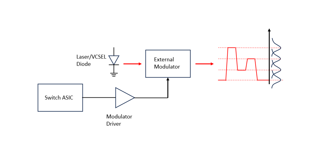
Silicon photonics is one of the hottest and fastest moving markets to address high speed data demands in co-packaged optics (CPO) in AI data centers.
In this post I’ll cover a few important high-level details of silicon photonic circuits. These include:
An Overview of the Link Budget and important considerations:
Laser Power
Connector Losses
Receiver Figures of Merit
🔒Key Figures of Merit for eye quality
🔒Validation Challenges (wafer screening and thermal stability)
Understanding link budgeting is important to develop a system level understanding of a SiPh transceiver. Consider a typical electro-optical link with an external modulator:
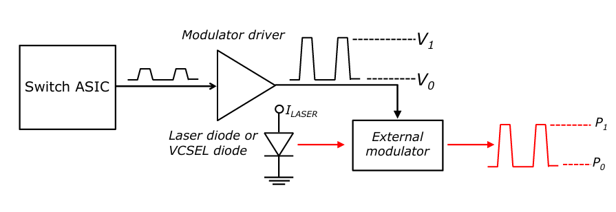
Figure 1. A typical external modulation scheme for NRZ. Source: Ossieur, P. “Introduction to Optical Communication Systems From VCSELs, integrated photonics to coherent solutions” ISSCC 2026
At a high level, the job of a transmitter is to transmit the data at the specified data rate (224GPBS) with as low BER as possible in the given specification. Key system level performance specs include:
Power efficiency: The ratio of energy consumed to the amount of data transmitted. This is usually measured in pJ/bit.
BER: Bit error rate. Noise, loss and other effects degrade bit error rate. Requirements range between 1e-4 and 1e-6 depending on the standard.
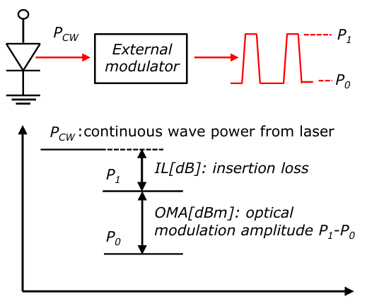
Figure 2. Sources of loss in the external modulator. Source: Ossieur, P. “Introduction to Optical Communication Systems From VCSELs, integrated photonics to coherent solutions” ISSCC 2026
A laser source (whether that be generated on board or coupled in externally) provides the power and is sent through a lossy modulator, connectors, and waveguides.
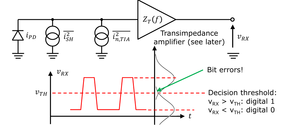
Figure 3. The RX side, where the photodetector converts the optical signal to a current and a transimpedance amplifier (TIA) amplifies this to a voltage. Source: Ossieur, P. “Introduction to Optical Communication Systems From VCSELs, integrated photonics to coherent solutions” ISSCC 2026
This power is then sent through the optical channel, converted back to a weak electrical signal through a photodetector, and amplified by a transimpedance amplifier. The signal at the RX need to be high enough compared to the noise in order to be able to detect the signal properly.
All of the sources of loss in between the TX and RX must be quantified for in a link budget in the optical chain. Lets break down each part.
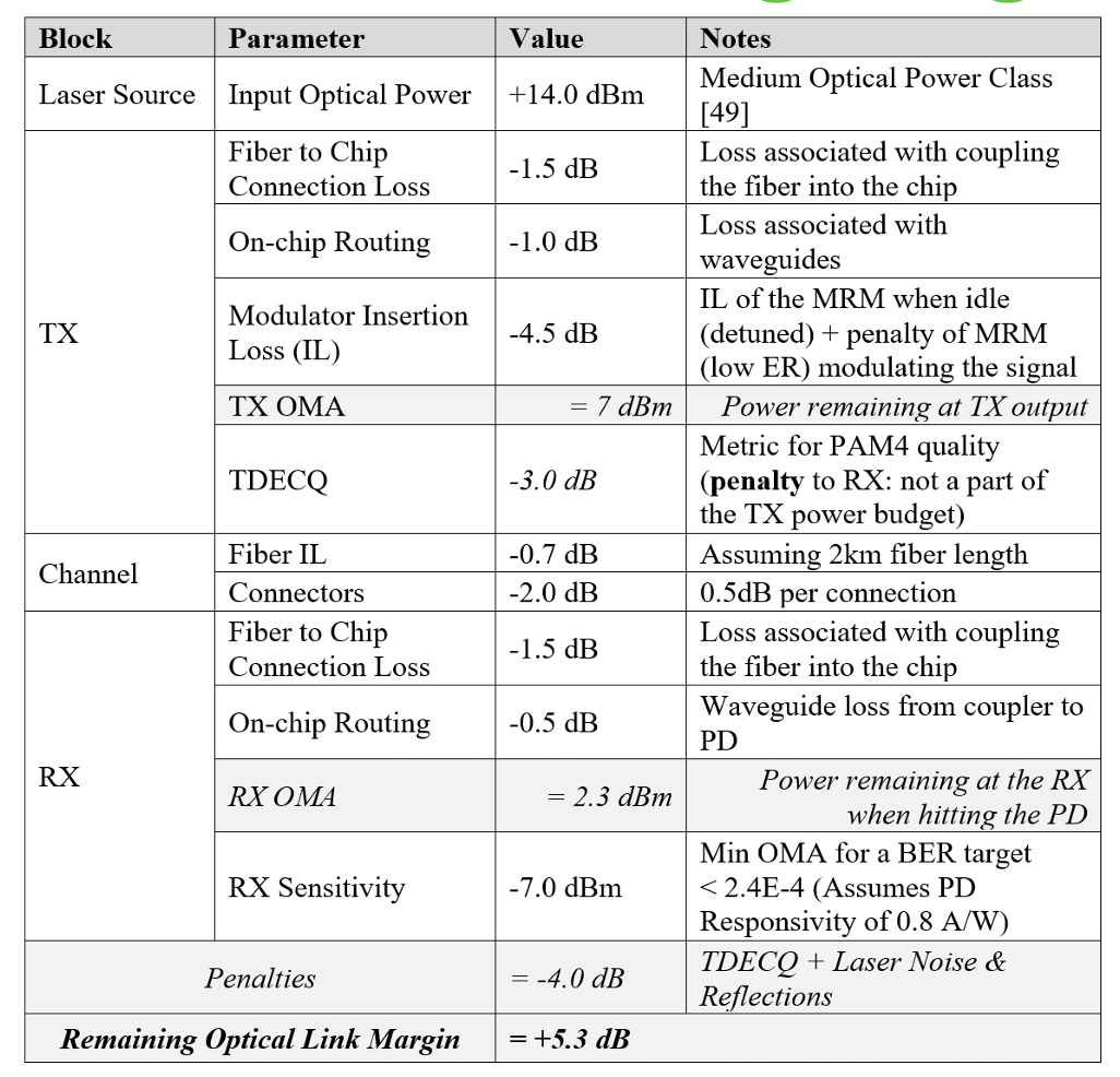
Figure 4. Example of a link budget and typical items. Source: Nourzad, M and Liu, Y. (Lightmatter) “Navigating the New Frontier: A Guide to Testing Silicon Photonics High-Speed Links” DesignCon 2026
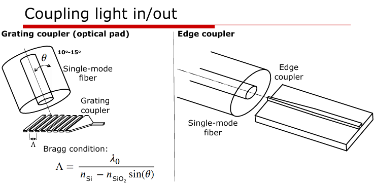
Figure 5. Methods to couple light into a SiPh circuit externally. Source: Aflatouni, F. “Silicon photonics-based solutions: components, circuits, and integration” ISSCC 2026
Lasers are either integrated within the PIC or coupled in externally. These external lasers are coupled into the chip through edge couplers or grating couplers.
There are a few important specifications:
- Power:The amount of coupled power is limited by two-photon absorptionand other non ideal effects. Shown is a sweep of Pin vs Pout where Pout saturates and a high enough Pin can cause passivation melting:
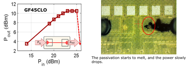
Figure 6. The Pout/Pin characteristics to couplers where the power saturations after a certain point. Source: Aflatouni, F. “Silicon photonics-based solutions: components, circuits, and integration” ISSCC 2026
- Relative intensity noise (RIN)- Rin refers to the relative intensity fluctuations of the optical signal of a laser source. This is a critically important parameterin PAM4 schemes because PAM4 has much lower noise margin than NRZ. A high RIN raises the noise floor causing a higher BER. RIN is given by:

Companies with lasers in the value chain include Lumentum, Broadcom, Coherent, Sivers, Scintil, Xscape, and Quintessent.
There are several loss sources in the connectors themselves. These include:
Modulator loss - due to intrinsic optical absorption and scattering
Multipath Interference (MPI) - Optical reflections from multiple connectors / discontinuities
Polarization Dependent Loss (PDL)- Measures loss due to change in signal polarization
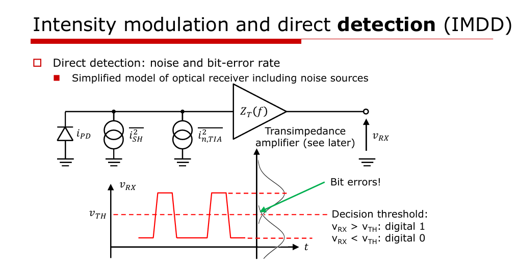
On the receive side, the signal is detected by a photodetector. This weak signal plus a noise signal is converted to a voltage through a transimpedance amplifier (TIA) that converts current to voltage.
A few key specs here are important:
Responsivity -Measures how effective the photodetector converts photons to electrons. This is typically measured in A/W.
Dark current -Measures the current flow when no light is present. Defects can cause high dark current that adds noise to RX and reduces sensitivity.
Input-referred noise - assesses the noise floor of the TIA.
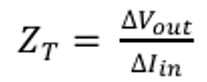
Transimpedance Gain - measures the electrical strength of the receiver. TIA gain is very important because if TIA gain is too low, output voltage swing will not be high enough to compensate for noise. It is given by:
- Receiver sensitivity- the minimum optical power required to achieve a specific BER target. This is determined by plotting RX BER vs OMA. BER goes down when received optical power goes up.
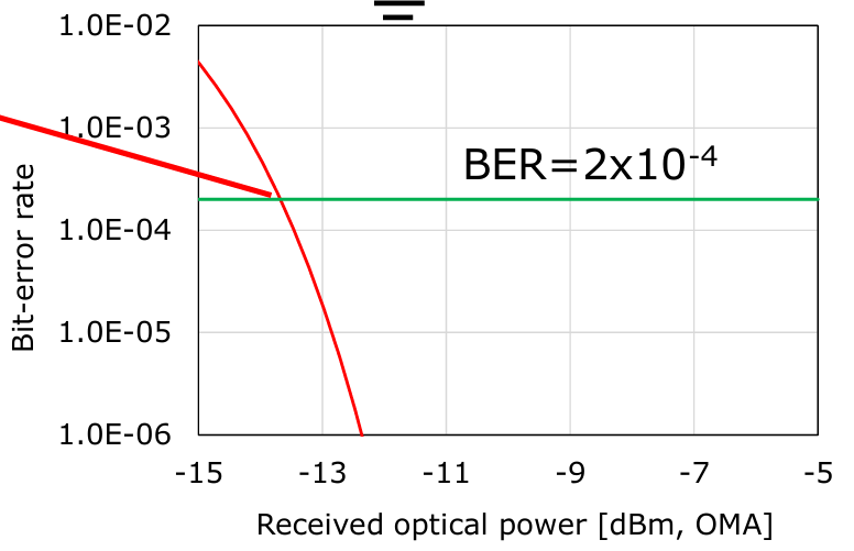
Figure 9. Received Optical power vs BER. Source: Ossieur, P. “Introduction to Optical Communication Systems From VCSELs, integrated photonics to coherent solutions” ISSCC 2026
- THD (Total Harmonic Distortion) - quantifies the non-linearity of the TIA. This affects PAM4 because it affects how even spaced out each of the four levels are after optical to electrical conversion.
After the paywall I’ll go into key parameters that define the eye quality, practical challenges when scaling production of SiPh, and NVIDIA’s approach to thermal tuning design.
⚠️ 以下为正文付费墙之后的内容(🔒 眼图质量关键 FOM / 🔒 量产验证挑战:晶圆筛片 wafer screening + 热稳定性 thermal stability + NVIDIA 热调谐设计)。jina 仅返回至上方 “After the paywall I’ll go into…” 处的免费预览,本发布未包含任何付费内容。
第二部分:解析(深度解读)
核心论点摘要
这是一篇面向 CPO(共封装光学)语境的硅光链路预算(link budget)系统级入门拆解。作者把一条典型”外调制电光链路”从 TX 到 RX 的每一段损耗与噪声源逐一定量,目的是建立对硅光收发器(silicon photonic transceiver)的系统级直觉——而不是陷进单个器件。
免费公开段覆盖了一条 224 Gbps(NRZ)链路的关键模块:
- 链路预算总览:TX→(调制器/连接器/波导损耗)→光信道→RX(PD→TIA)全链路的所有损耗源都要在 link budget 里逐项量化(Figure 4 给了 Lightmatter 在 DesignCon 2026 给出的典型表项)。
- 发射端指标:功耗效率(pJ/bit)与 BER(标准从 1e-4 到 1e-6)。
- 激光功率:①耦合功率受双光子吸收(two-photon absorption)限制,Pout 随 Pin 提升会饱和,Pin 过高甚至会熔融钝化层(passivation melting);②RIN(相对强度噪声)——作者特别强调这是 PAM4 的关键参数,因为 PAM4 噪声裕度远低于 NRZ,高 RIN 抬高噪声基底 → BER 升高。
- 连接器损耗:调制器本征吸收/散射损耗、MPI(多径干涉)、PDL(偏振相关损耗)。
- 接收端 FOM:响应度(responsivity, A/W)、暗电流(dark current)、输入参考噪声(input-referred noise)、TIA 增益(transimpedance gain)、接收灵敏度(receiver sensitivity)、THD(总谐波失真,影响 PAM4 四电平均匀性)。
文末明确划出付费墙:眼图质量关键 FOM、量产验证挑战(晶圆筛片 + 热稳定性 + NVIDIA 热调谐设计)全部在墙后。也就是说,本文把”链路预算怎么算”讲透了,但”算完之后怎么在量产上兜住(尤其是热调谐)”这个对投资更关键的问题,被留在了付费段。
关键概念解读
- 链路预算(link budget):把 TX 到 RX 之间所有增益与损耗(调制器、连接器、波导、耦合、光纤、PD 灵敏度余量)逐项相加减,看接收端是否还有足够的 OMA(光调制幅度)裕度达到目标 BER。这是系统设计的”账本”。Figure 4 给出了典型表项模板。
- 双光子吸收(two-photon absorption):硅在高光强下的非线性吸收,是硅波导/耦合功率的上限来源之一。它导致 Pout 饱和(Figure 6),功率再往上不仅不增益,还可能烧熔融钝化层——这直接框定了单波可耦合进 PIC 的光功率上限,是 CPO 光源功率预算的硬约束。
- RIN 与 PAM4 的耦合:PAM4 用 4 个电平传 2 bit,每个电平间隔只有 NRZ 的 1/3,噪声裕度小得多。激光的 RIN 一旦抬高噪声基底,最外两电平最先被误判 → BER 飙升。所以外置 CW 激光源的 RIN 规格(如 Lumentum 的 UHP DFB)是 CPO 链路能否跑 PAM4 的命门。
- MPI(多径干涉)/ PDL(偏振相关损耗):都是连接器/不连续处的反射与偏振效应带来的额外损耗与眼图退化。在封装内高密度、多 connector 的 CPO 环境里会被放大,是良率与一致性的隐患。
- 接收端 FOM 串:responsivity 决定 PD 把光转成电流的本领;dark current 是”无光也漏电”,缺陷会抬高 RX 噪声、压低灵敏度;input-referred noise 是 TIA 噪声基底;TIA gain 把微弱电流放大到能压过噪声的电压摆幅;receiver sensitivity 是达到目标 BER 所需的最小光功率(BER 随接收光功率升高而下降,Figure 9);THD 衡量 TIA 非线性,直接决定 PAM4 四电平是否等间隔。
- 热调谐(thermal tuning):被作者列为付费段的”NVIDIA 方案”核心。硅光器件对温度极敏感(相位、谐振波长漂移),量产一致性要靠热调谐/热稳定来兜——这恰好是 CPO 可制造性的”最后一公里”。
投资逻辑(与本站的连接)
这篇文章是本站 CPO 系统级”账本” 的拼图——它把上游光源、中游调制/耦合、下游探测,统一收进一条 link budget:
- 《Lasers for CPO/NPO: Part 1 – InP DFB 激光器》 与 《Part 2 – Lumentum 的技术与护城河》:本文的”激光功率 / RIN”段正是那两篇的系统级出口——UHP CW 激光器的功率上限(双光子吸收)与 RIN 规格,最终都要在 link budget 里被”消费”掉。RIN 对 PAM4 的致命性,反向印证了 Lumentum 高功率窄线宽 DFB 的价值。
- 《CPO 测试瓶颈 / 100 秒瓶颈》:本文付费段的 “wafer screening(晶圆筛片)” 与 “thermal stability(热稳定性)” 验证挑战,正是 CPO 量产测试栈要解决的核心问题——link budget 算得再漂亮,芯片级一致性(热漂移、暗电流分布、RIN 一致性)也要靠测试兜住。
- 《为什么你该关注光测试赛道》:晶圆筛片 + 热稳定性验证 = 测试设备最先兑现收入的环节;本文把”为什么需要测”从物理上交代清楚了。
- 《CPO 共封装光学 primer(Part 3)》:本文的 TX/RX 链路图、耦合方式(edge/grating coupler,Figure 5)是该 primer 的器件级实例。
- 《TSMC 领先 CPO / 三星第三颗芯片》:封装内光 I/O 的良率,本质上取决于本文所列每一段损耗/噪声的工艺一致性——link budget 是封装厂与光引擎厂的”共同语言”。
- 一句话:本文免费段给了 CPO 链路的完整物理账本;但”账本算完、量产如何兜住(尤其是 NVIDIA 热调谐)”这个对估值更关键的问题在付费墙后,当前不宜据此对单一环节做单向押注。
风险提示
- 本文为 Silicon Codesign 免费公开部分,止于文末 “After the paywall I’ll go into…“。🔒 眼图质量关键 FOM、🔒 量产验证挑战(晶圆筛片 + 热稳定性 + NVIDIA 热调谐设计) 均位于付费墙之后,本发布未含任何付费内容。
- 文中图表多引自 ISSCC 2026 / DesignCon 2026 公开讲稿(Ossieur、Aflatouni、Nourzad & Liu (Lightmatter)),为教学示意,具体产品参数以各厂商官方为准。
- 原文发布于 2026-05-20(署名 Silicon Codesign),与本站发布日(2026-07-23)不同;本文
date字段取本站发布日以符合站点排序惯例。 - 激光价值链公司(Lumentum、Broadcom、Coherent、Sivers、Scintil、Xscape、Quintessent)为原文列举,非投资建议;提及不构成对任一标的的推荐。