Optics Primer, Part 3: Co-Packaged Optics (CPO) — 共封装光学 CPO 入门:从 EML/DSP 到硅光与外部 CW 激光
整理自 ChipStrat (Substack) 的免费入门系列第 3 篇:从可插拔→LRO/LPO 一路走到 CPO。拆解 NPO 与 CPO 的物理差异、XSR SerDes 省电逻辑、硅光引擎与外部 CW 激光如何取代 EML+DSP、可维护性与可靠性反直觉改善、以及价值链从 InP EML/DSP 向硅光/CW 激光/先进封装的迁移。英文原文(全文免费)+ 中文深度解读。
本文整理自 ChipStrat (Substack) 的免费专栏文章,原文发布于 2026-03-09(作者署名为 Austin Lyons)。 标题原文:Optics Primer, Part 3: Co-Packaged Optics (CPO)。 结构为 正文(英文原文)+ 解析(中文深度解读),方便中英对照阅读。 本文为免费全文(ChipStrat 对该篇未设付费墙,文中仅末尾提示「深度公司级分析需订阅」),已完整转载正文与图示;订阅/推广按钮、关联文章推荐卡、读者头像等 UI 元素已略去。著作权归原作者所有,建议在 Substack 支持订阅。
第一部分:正文(Original Article)
Optics Primer, Part 3: Co-Packaged Optics (CPO)
From EML lasers and DSPs to silicon photonics and external CW lasers. How CPO works and the impact on the optical supply chain.
Mar 09, 2026
This series has been walking through the different ways datacenters connect optics to switch silicon, from pluggable transceivers to LRO to LPO. (See Optics Primer, Part 1: Traditional Pluggable Optics and Optics Primer, Part 2: LRO & LPO.)
If you haven’t read those, they are easy reads. I recommend skimming through them first.
Each step trades flexibility for efficiency. And the root source of the inefficiency is that long, noisy copper trace between the switch and the optics:
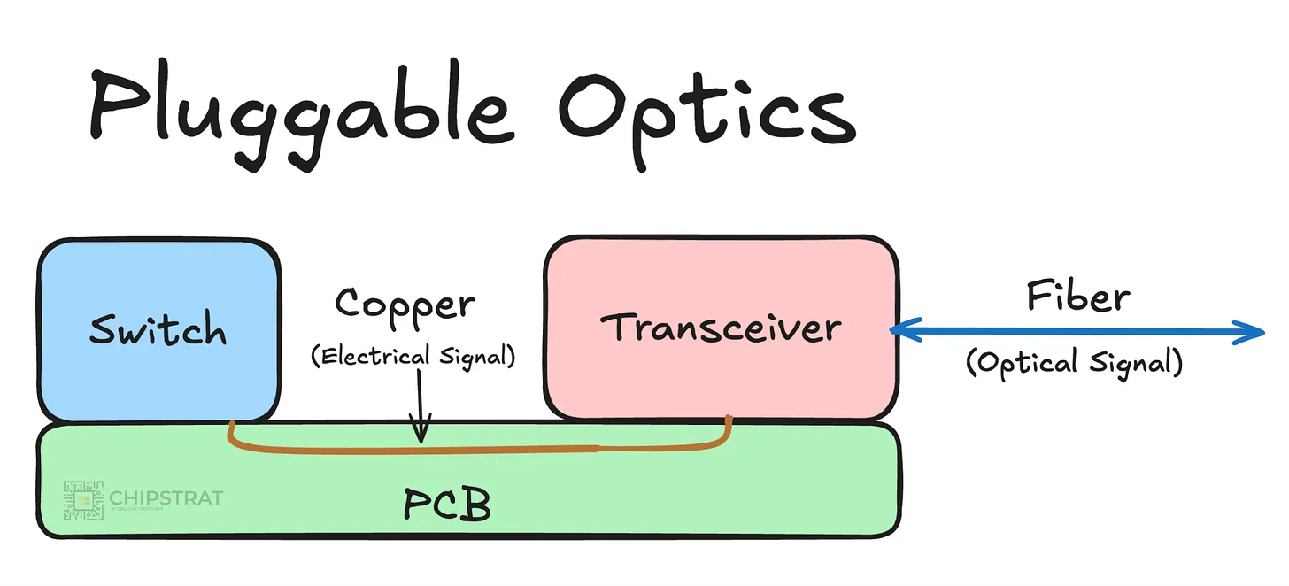
At modern lane rates (e.g 50G, 100G per lane), electrical signals pick up a ton of noise and distortion crossing the copper trace between the switch and the transceiver. Pluggable optics handle this with a DSP that overcomes the noise during transmit and receive. And LRO and LPO save power by relocating that DSP into the switch:
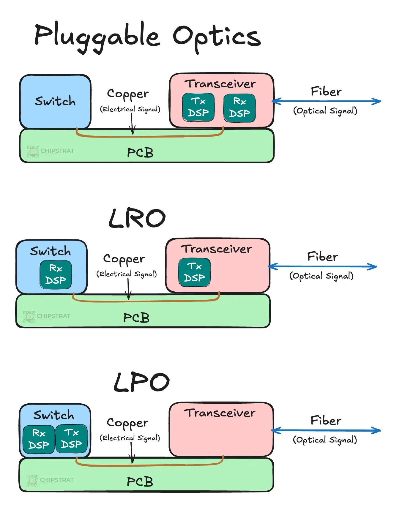
But the system becomes less modular and harder to mix-and-match. But why deal with that copper trace at all? What happens when you just… put the optics right next to the silicon?
NPO
Near package optics (NPO) brings the optics module on the same substrate or very close to the switch package, but not inside it:
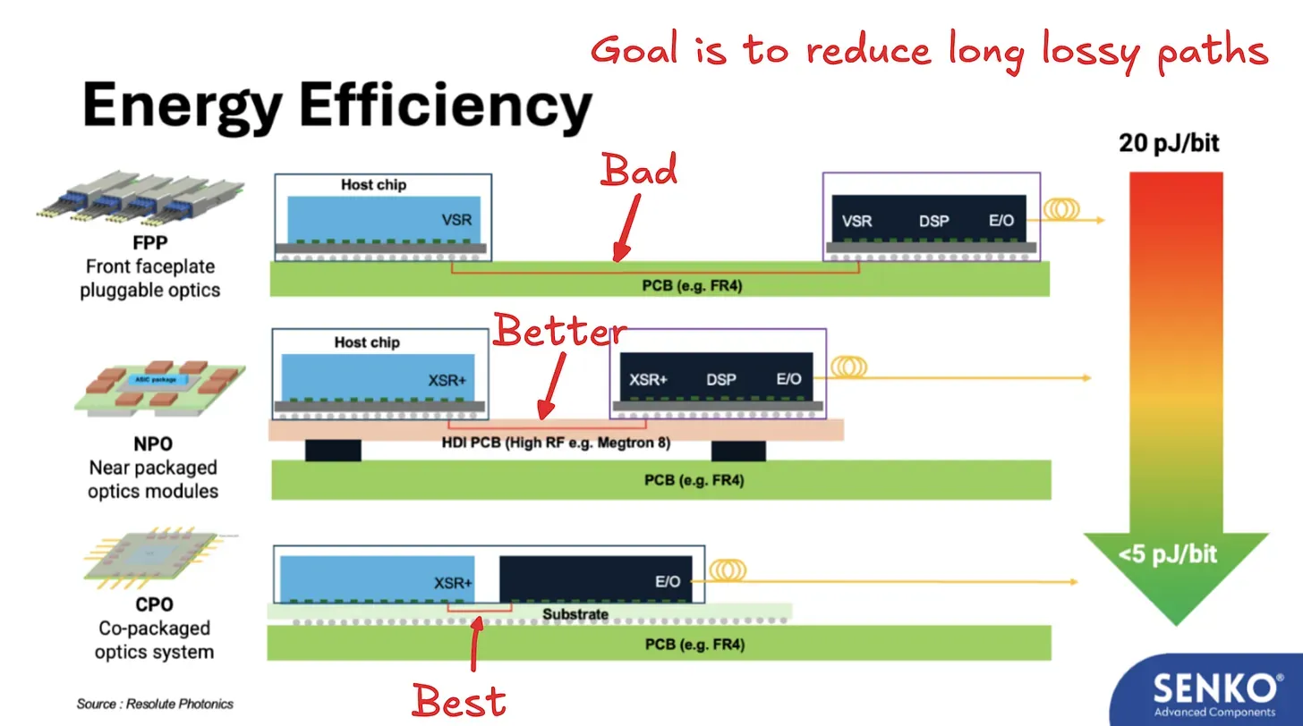
It’s close enough to reduce most copper impairments. This is a pragmatic middle ground, but the major players are largely leapfrogging it and going straight to CPO.
Might as well just reduce the copper distance to nearly zero right?
CPO
Finally! Co-packaged optics (CPO).
The optics move onto (or into) the switch package itself:
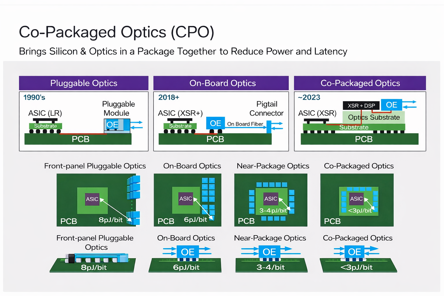
Cleaned up version of the following low-res image: Source
The electrical path between the switch die and the optical engine is now very short (millimeters or less). Since there’s no long copper trace, we needn’t have a DSP to compensate for it! Less silicon content, and less power.
There’s also much less SerDes power overhead as you only need extra short-reach (XSR) SerDes, the simplest, lowest-power tier:
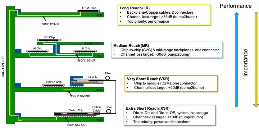
The simplest way to think about CPO is that the transceiver disappears and the optical engine moves onto the switch package itself.
How It Works
SemiAnalysis has an in-depth CPO article with a helpful diagram:
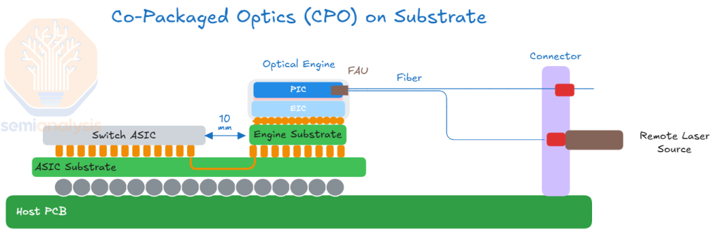
The optical engine is the core of CPO; it converts between the optical and electrical domains. Since the OE is on-package, fiber runs directly to the package edge. And now the electrical path to the switch is so short that signals stay clean without heavy conditioning. The switch ASIC’s SerDes handles what little remains.
Another helpful diagram from Nvidia’s blog. The red circles highlight noisy copper channels. Notice how CPO eliminates most of them:
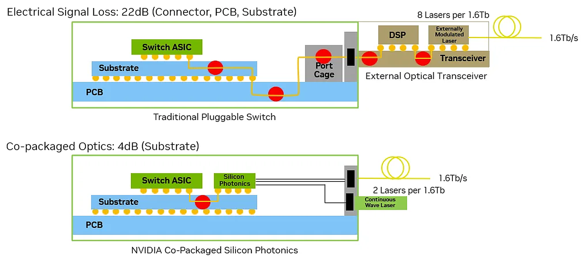
CPO cuts down on the overall power consumption, too. Per this example from Nvidia, power consumption cuts down from 30W for pluggables to 9W for CPO:
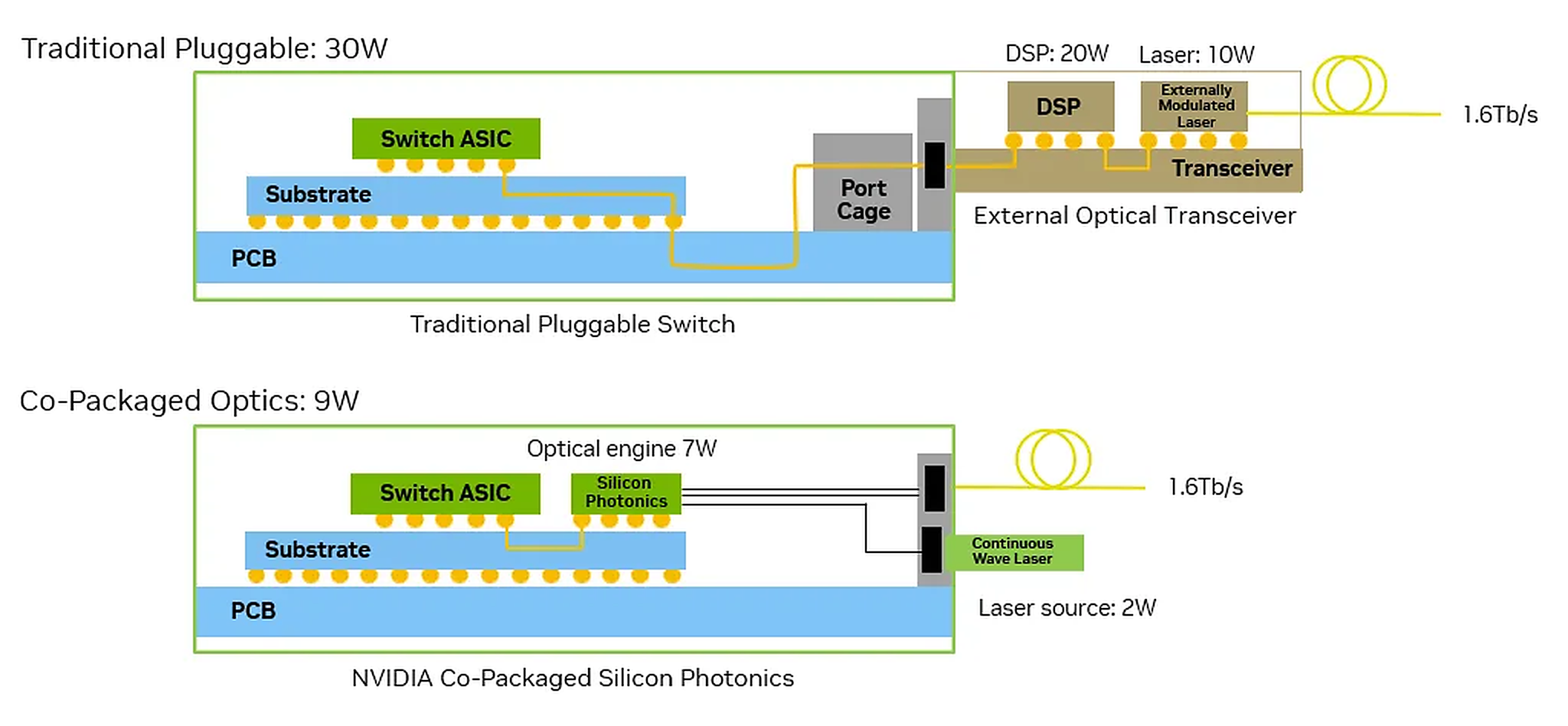
As I always say, in this power-constrained era, every watt saved is a watt that can be used for computation.
At this point, you should watch this Nvidia CPO video again, as it will make a lot of sense now:
- Nvidia CPO video: youtube.com/watch?v=kS8r7UcexJU
Lasers and Silicon Photonics
Oh yeah, an important call out. Look at the Nvidia diagrams above again. The pluggable transceiver uses externally modulated lasers (EMLs) for 1.6Tb. These are discrete InP lasers + modulators.
CPO uses lasers differently. Instead of modulating the laser itself, it uses a simple continuous wave (CW) laser (just a constant beam of light) and performs the modulation on a silicon photonics chip on the switch substrate:
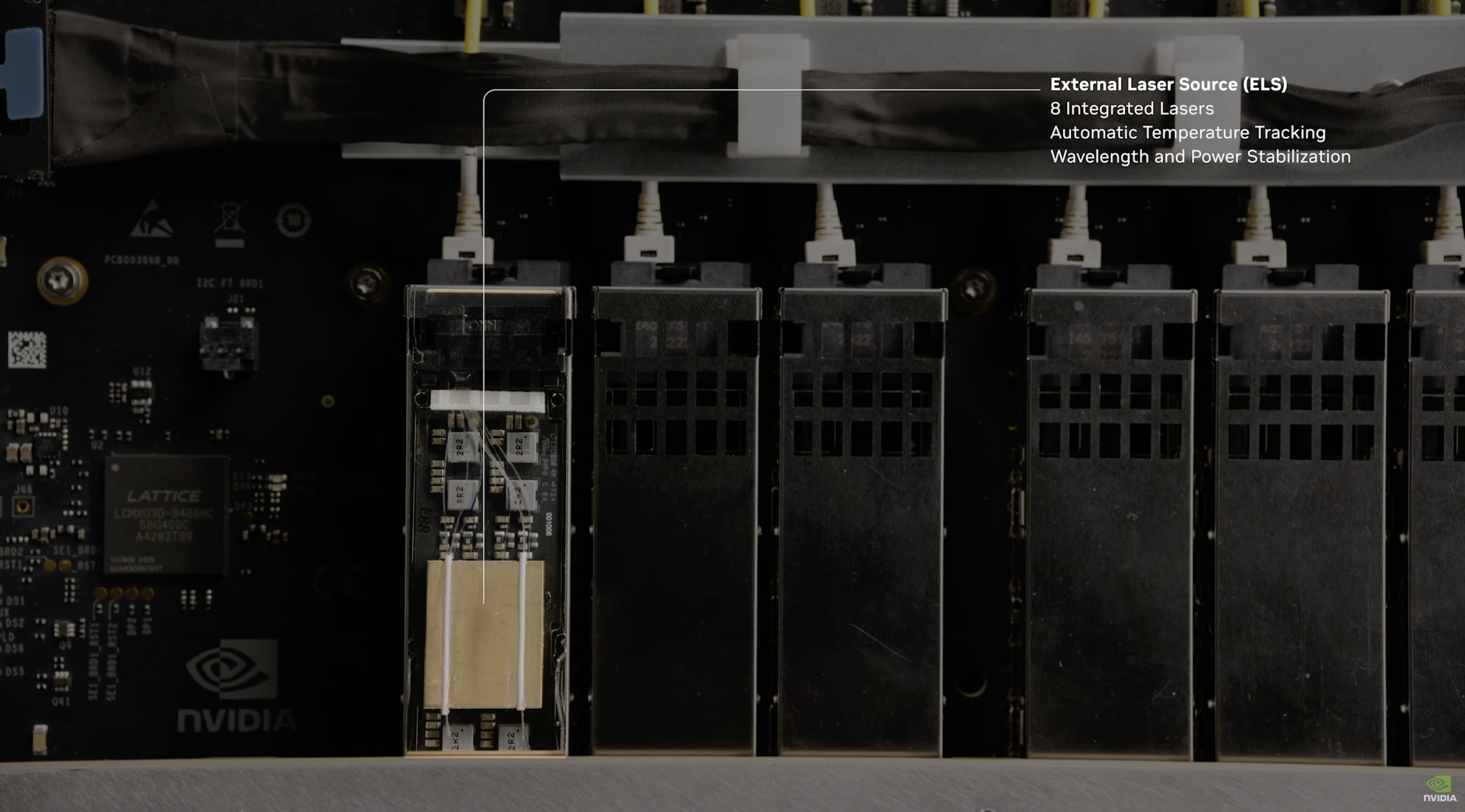
Nvidia’s external CW laser
Silicon photonics is an optical circuit built in silicon using CMOS-compatible fabrication of waveguides, modulators, photodetectors:
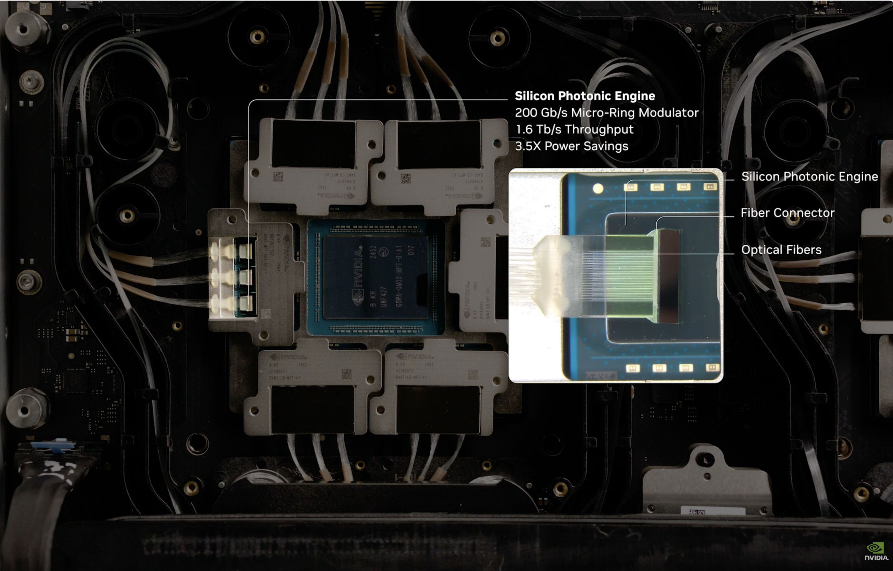
Nvidia’s silicon photonics
What about serviceability though? Don’t lasers fail?
Yes, and this was one of the earliest objections to CPO. In pluggable optics, a failed laser means swapping the transceiver module which is easy to access. But if the laser is near the switch… that’s a lot harder right?
Well, don’t put the laser near the switch! The CW laser is external. So if it fails, you can still easily replace the laser source and not the switch.
And as Nvidia shows here, the silicon photonic engines themselves are designed as detachable sub-assemblies. Not as easy as swapping a front-panel pluggable, but far better than scrapping the switch:
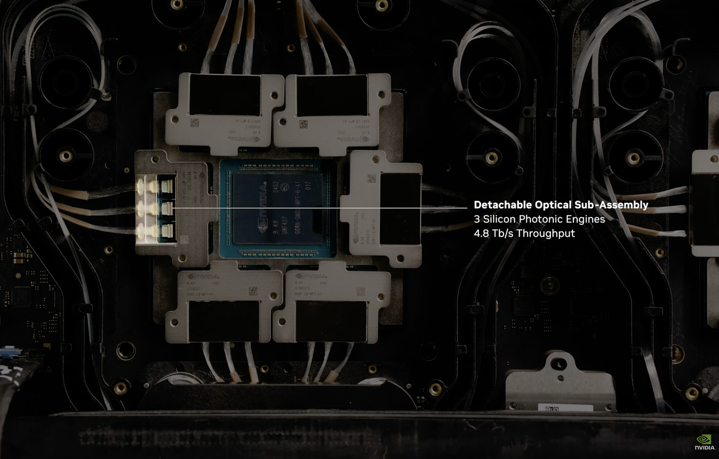
Thermal concerns are similar. Lasers are temperature-sensitive and switch ASICs run hot; pluggable EMLs combine a laser and modulator in a single InP device running at high speed, and they run hot and are among the more failure-prone components.
But with CPO, the laser is just a simple CW source and the high-speed modulation moves to silicon photonics. If the laser sits off-package, you’ve removed the most temperature-sensitive component from the equation!
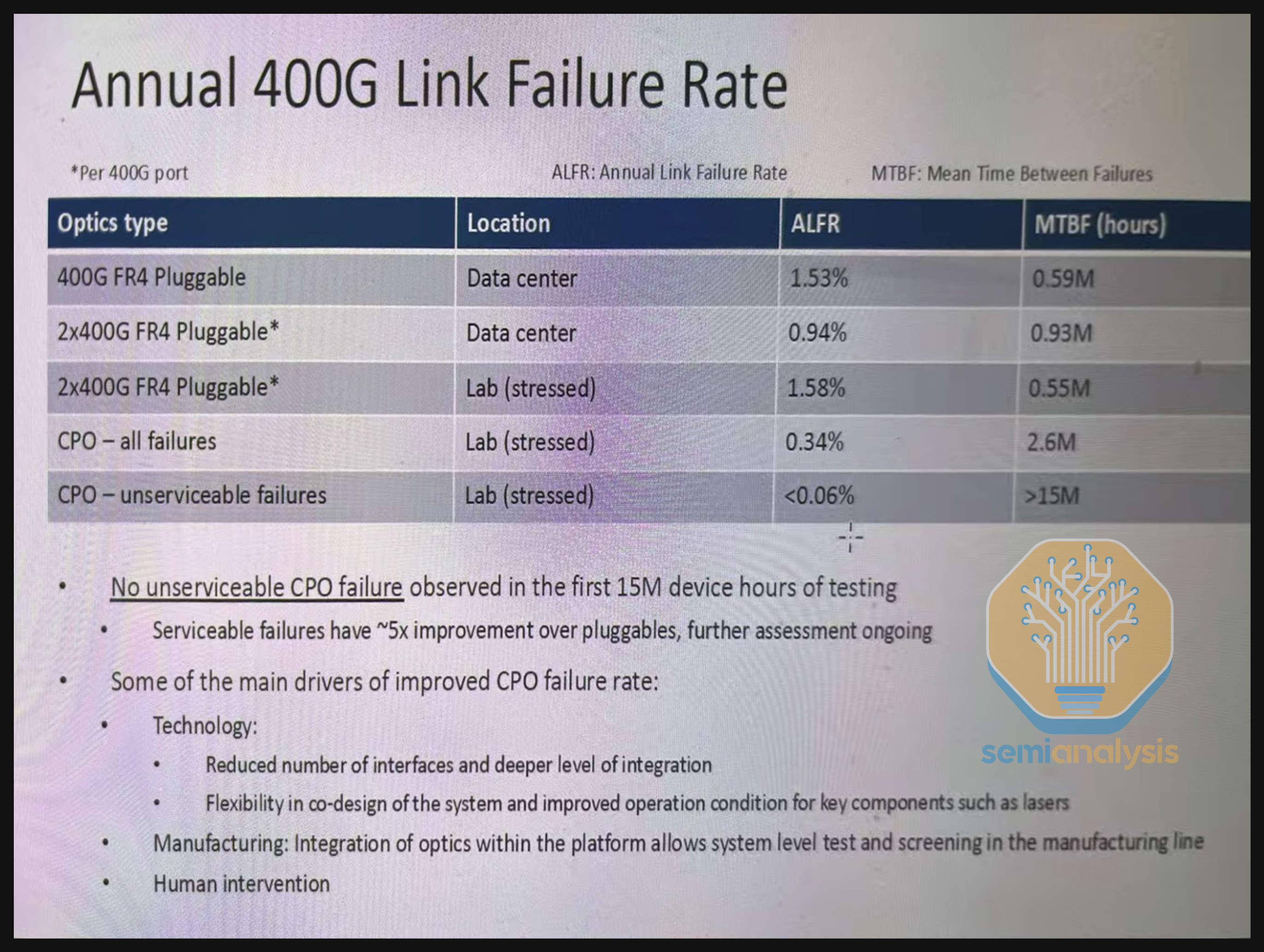
Moving optics closer to the switch looked like a reliability problem, but it may end up improving reliability instead. In fact, SemiAnalysis shared this nice slide from Meta that suggests Meta had fewer failures using CPO than with pluggables:
Trade-offs
Everything in engineering is about trade-offs, and CPO is no different.
Manufacturing is non-trivial. The silicon photonics engines sit very close to the switch ASIC, which means integrating optical and electrical components with different materials, process flows, and reliability characteristics. That complicates packaging, thermal design, and testing compared with traditional pluggable optics.
And CPO also tightens the coupling between the optics and the switch platform. With pluggables, operators can mix transceiver vendors or change optical reaches independently of the switch. In a CPO system, the optical engines are designed and qualified as part of the switch platform, which reduces that flexibility.
But that’s a manageable trade for hyperscalers, who co-design systems with their silicon partners (Broadcom, Marvell), control board layout and qualification, and deploy into environments they fully manage.
And Nvidia is bringing CPO to its merchant switch lineup (Spectrum-X Photonics, Quantum-X Photonics), which could eventually bring CPO within reach of non-hyperscalers who don’t have that kind of vertical integration. Well, they do have that kind of vertical integration… via Nvidia.
Pluggables Are Not Dead
Pluggable transceivers are EML-based InP modules with DSPs. As CPO scales, we need more silicon photonics engines and CW laser sources, and fewer DSP chips for pluggables.
People like to jump to conclusions. Remember: Copper is dead! Long live optical!
But as Vik and I discussed recently, I’d sum it up as: The answer is both. The question is when.
- Discussion video: youtube.com/watch?v=47cQTPjDUB8
Yes, the direction of travel is toward tighter integration of optics and silicon. But the debate is how fast. After all, Hock Tan claimed 400G SerDes on the last Broadcom earnings call, which would extend the pluggable runway. But Broadcom is also shipping early-access CPO switches. Nvidia is shipping CPO in 2026. Marvell acquired Celestial AI to get in the game.
Today, pluggable optics concentrate value in the transceiver module. InP EML lasers, DSPs, driver and TIA chips, optical packaging. Companies like Lumentum, Coherent, Fabrinet, and DSP suppliers like Marvell and Broadcom sit in that value chain.
But with CPO, there’s an unbundling in the value chain. The optical functions move onto the switch package as silicon photonics engines, the laser becomes a separate CW source, and the DSP largely goes away.
Hence, value shifts toward silicon photonics, CW laser production, and advanced packaging, and away from standalone transceiver DSPs and pluggable module assembly.
But again, these shifts are happening over time. As I said in the video above, the transition between technologies isn’t just a binary thing on a particular date, but more of an adoption curve. Even a single hyperscaler can be deploying different technologies at different places at roughly the same time. So pluggables are still a great business.
I’ve already started pulling on these value chain threads. If you want to understand the laser side in depth, check out Lumentum and the Laser Bottleneck and Broadcom Makes Lasers, which are both directly connected to the CW laser and silicon photonics shifts we covered here. And more to come! Coherent, Applied Optoelectronics, Astera, Poet, etc. Getting lots of requests from readers :)
第二部分:解析(深度解读)
以下为中文解读,帮助没有光通信背景的读者抓住主线;技术细节以第一部分英文原文为准。
一、核心论点摘要
这篇是 ChipStrat「光通信入门」系列的第 3 篇,定位是科普而非深度投资,但它把 CPO 的「为什么」讲得非常干净:
- 一切低效的根源是那根又长又吵的铜走线(switch ASIC ↔ 可插拔光模块之间)。可插拔靠 DSP 去噪、LRO/LPO 把 DSP 挪进交换机省电,但都没消灭这根铜线。
- CPO 把光引擎直接搬上(或进)交换机封装,铜走线缩短到毫米级 → 不再需要 DSP 补偿 → 更少硅、更少功耗;SerDes 也只需最省电的 XSR 短距层。
- 激光器与调制解耦:可插拔用「InP EML(激光器+调制器合一)」;CPO 改用「外部 CW 连续波激光 + 硅光芯片上调制」。激光放封装外,可单独更换,反而改善了可维护性。
- 可靠性是反直觉的:把光拉近交换机看似更脆弱,但最怕热的激光器被移出封装、高速调制移到硅光,Meta 实测 CPO 故障率比可插拔更低。
- 可插拔没死:价值链在「解绑」——价值从 InP EML/DSP/模块组装,转向硅光、CW 激光、先进封装;但这是一条 adoption curve,不是某天一键切换,可插拔仍是好生意。
二、关键概念解读
- NPO(Near-Package Optics,近封装光学):光模块放在同一基板或贴着封装,但不在封装内。足够近、能消掉大部分铜损,是务实折中;但大厂多数选择跳过 NPO 直奔 CPO。
- CPO(Co-Packaged Optics,共封装光学):光引擎在封装上/内,switch die 到光引擎的电气路径仅毫米级,本质就是「收发器消失」。
- XSR SerDes:极短距 SerDes,是 SerDes 各档里最简单、最低功耗的一档。CPO 只需 XSR 连接 die 与光引擎,省掉了长距/中距 SerDes 的功耗开销。
- EML(Externally Modulated Laser,外调制激光器):InP 激光器与调制器合一的高速器件,可插拔 1.6Tb 的主力;缺点是「激光+调制」同在一个高速发热的 InP 器件里,是故障高发件。
- CW 激光(Continuous Wave,连续波激光):只发一束恒定光,不做调制;调制交给硅光芯片。它简单、可置于封装外,是 CPO 可靠性改善的关键。
- 硅光(Silicon Photonics):用 CMOS 兼容工艺在硅上做波导、调制器、光电探测器的「光路」。它是 CPO 的价值归集点。
三、分层对比表
三种形态:从铜到光的递进
| 形态 | 光的位置 | 铜走线 | DSP 位置 | 灵活性 | 能效 |
|---|---|---|---|---|---|
| 可插拔(Pluggable) | 前面板模块 | 长(跨板) | 模块内 | 最高(可混插 vendor) | 基准(~30W 示例) |
| LRO / LPO | 前面板模块 | 长(跨板) | 移入交换机 / 去掉 | 下降 | 较好 |
| NPO | 同基板/贴封装 | 很短 | 视设计 | 中 | 好 |
| CPO | 封装上/内 | 毫米级 | 基本不需要 | 最低(与平台绑定) | 最佳(~9W 示例) |
激光器范式对比
| 可插拔 EML | CPO CW + 硅光 | |
|---|---|---|
| 激光器件 | InP 激光+调制合一 | 外部 CW 激光(恒定光) |
| 调制位置 | 激光器内部 | 硅光芯片上 |
| 失效更换 | 换整个模块 | 换外部激光源 / 可拆卸硅光引擎 |
| 热敏感件 | 在封装内高速发热 | 移出封装,最热敏件被移除 |
| 故障率(Meta 实测) | 基准 | 更低 |
四、技术趋势与产业视角
- 「收发器消失」是封装范式的转移:价值从「模块组装」沉到「晶圆级硅光 + 外部激光 + 先进封装」。这与本站已发的 三星第三颗芯片 指向同一方向——光正从面板挪进封装、再向 XPU-HBM 封装内光 I/O 演进。
- 可维护性焦虑被化解:早年反对 CPO 的最大理由是「激光坏了怎么办」;本文点出答案——激光本就不该在封装里(外部 CW),硅光引擎做成可拆卸子组件,比报废整机好得多。
- 「方向对 ≠ 节奏对」:作者反复强调这是 adoption curve 而非某日切换;Broadcom 说 400G SerDes(延长可插拔寿命)的同时也在送样 CPO,NVIDIA 2026 年出货 CPO,Marvell 收购 Celestial AI 入局。这与 The Illusion of CPO 的「坐标才分高下」互为呼应——两个视角(科普入门 vs 深度落地坐标系)互补。
- 价值链解绑的受益/受损方:受损——独立收发器 DSP、可插拔模块组装;受益——硅光代工/设计、CW 激光产能、先进封装。文中点名的既有玩家:Lumentum、Coherent、Fabrinet(可插拔链),Marvell、Broadcom(DSP 兼 CPO)。
五、与本站其他文章的连接
- The 100-Second Bottleneck Behind NVIDIA’s CPO — NVIDIA CPO 出货与瓶颈的浓缩版,可配合本文「30W→9W」的功耗论点。
- TSMC Is Ahead in CPO. Samsung Is Putting a Third Chip Next to HBM — 从「交换机 CPO」延伸到「XPU-HBM 封装内光 I/O」,是本文「CPO 只是起点」的产业纵深。
- The Illusion of CPO [CPO Special Final] — 深度落地坐标系(六大瓶颈、代工厂三足、玩家图谱),与本文科普视角互补。
- Why You Should Be Watching Optical Test — 本文点到的「testing 比可插拔更复杂」,在光测试一文中展开为具体投资线索。
- 光投资地图 v1.0 — 把本文「价值链解绑」映射到可关注的公司与环节。
六、风险提示
- 本文为入门科普,不含公司级财务/产能深解(作者明确说深度公司分析需订阅),投资判断请勿仅凭此篇。
- CPO 仍是 adoption curve,节奏受 400G/800G SerDes、良率、液冷渗透、 hyperscaler 共设计节奏影响;「可插拔没死」是作者反复强调的 caveat。
- 标的中涉及的 Lumentum、Coherent、Fabrinet、Marvell、Broadcom 等,其 CPO 相关营收占比与节奏差异极大,需结合各自财报与路线图独立验证。
- 本发布仅作信息整理与学习用途,不构成任何投资建议。