Why You Should Be Watching Optical Test Right Now — 光测试赛道的投资逻辑与五大瓶颈
整理自 Damnang 的 CPO 投资分析:拆解光测试价值链条的 5 大瓶颈,解析不同渗透情景下哪些设备公司最先兑现收益。英文原文 + 中文解读。
本文整理自 Damnang (Substack) 的科技投资分析文章,原文发布于 2026-05-03。 结构为 正文(英文原文)+ 解析(中文深度解读),方便中英对照阅读。
第一部分:正文(Original Article)
Why You Should Be Watching Optical Test Right Now
Who Makes Money First Across 5 Bottlenecks

来源:Damnang (Substack) · 2026-05-03
Since publishing the Optical Investment Map, I’ve heard from a lot of readers. The common thread: the optical theme has already run up significantly, and it was hard to know which names to look at or how to approach them. The investment map helped by laying out the full value chain and the competitive dynamics at each layer. What I found most rewarding was hearing that people used it not just to pick individual stocks, but to build their own investment strategy and portfolio.
But if you look closely at that map, there was one layer among the seven that clearly stood apart.
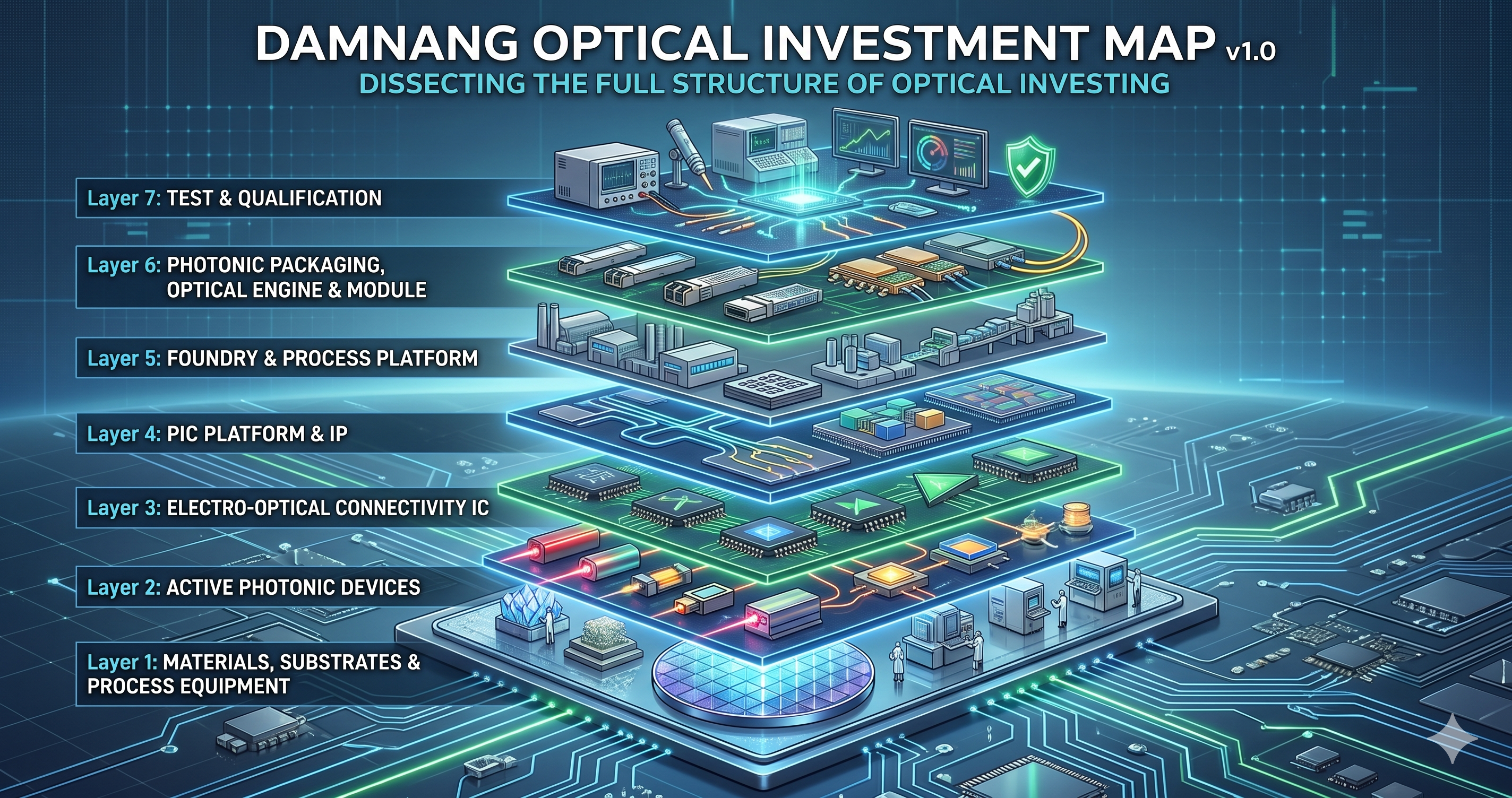
Layer 7: Test.
Layers 1 through 6 are fundamentally about making and moving light. You lay down materials, build lasers, design PICs, package them, and assemble modules. Each layer connects naturally to the ones above and below.
Test is different. Test sits outside this flow and cuts across every stage. You need testing at the wafer level, the package level, and the system level. The customers are different, the cycles are different, and the competitive landscape is different. It’s far too broad and deep to compress into a few lines within a single layer.
As an engineer who studied semiconductor test and works in Silicon Valley doing test and silicon debug, I’m convinced that optical test, specifically CPO test, is the area that demands attention right now. As optics move inside the package, the complexity and cost of test are structurally changing. And this shift is not yet fully reflected in the market.
In this article, I’m pulling Layer 7 out of the Optical Investment Map and analyzing it separately. The point is not simply to list test equipment companies. It’s to work through which bottlenecks open first under different CPO adoption scenarios, and which companies can capture the economics of those bottlenecks.
To do this, I break the optical test value chain into 5 bottlenecks and evaluate 14 stocks across 6 investment Factors. This is not a single ranking. The stocks you should watch change depending on which CPO scenario you believe in.
This article is based on publicly available information and general industry knowledge. It does not contain any NDA-protected or confidential information from any company, and is not a buy or sell recommendation.
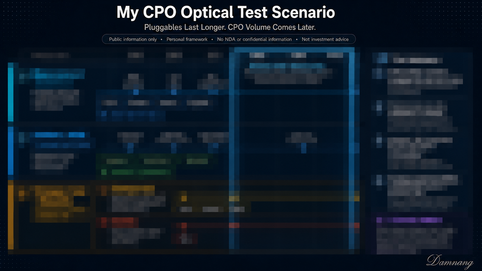
本文所引用的母图(Optical Investment Map v1.0,7 层价值链,Test = Layer 7):
Why CPO Test Matters Right Now
The direction of optical interconnects is already set. The path goes from pluggable to NPO, and ultimately to CPO. The closer the optical engine moves to the ASIC, the better the power efficiency and bandwidth density.
As of 2026, 800G pluggables are in high volume and 1.6T is ramping. Up through this stage, existing test infrastructure can handle the workload. You test the ASIC on its own, and the module maker tests the optical module separately.
But CPO is a different game.
When the PIC moves inside the ASIC package, the economics of test change. With pluggables, if you get a bad optical module, you pull it out and swap it. But in CPO, the PIC, EIC, and switch ASIC are bonded together inside a single package. If a PIC defect is discovered late, you may have to scrap the entire expensive ASIC package. That’s why securing Known Good Die from the PIC before packaging becomes a critical prerequisite for CPO mass production.
This shift matters for test equipment companies for three reasons.
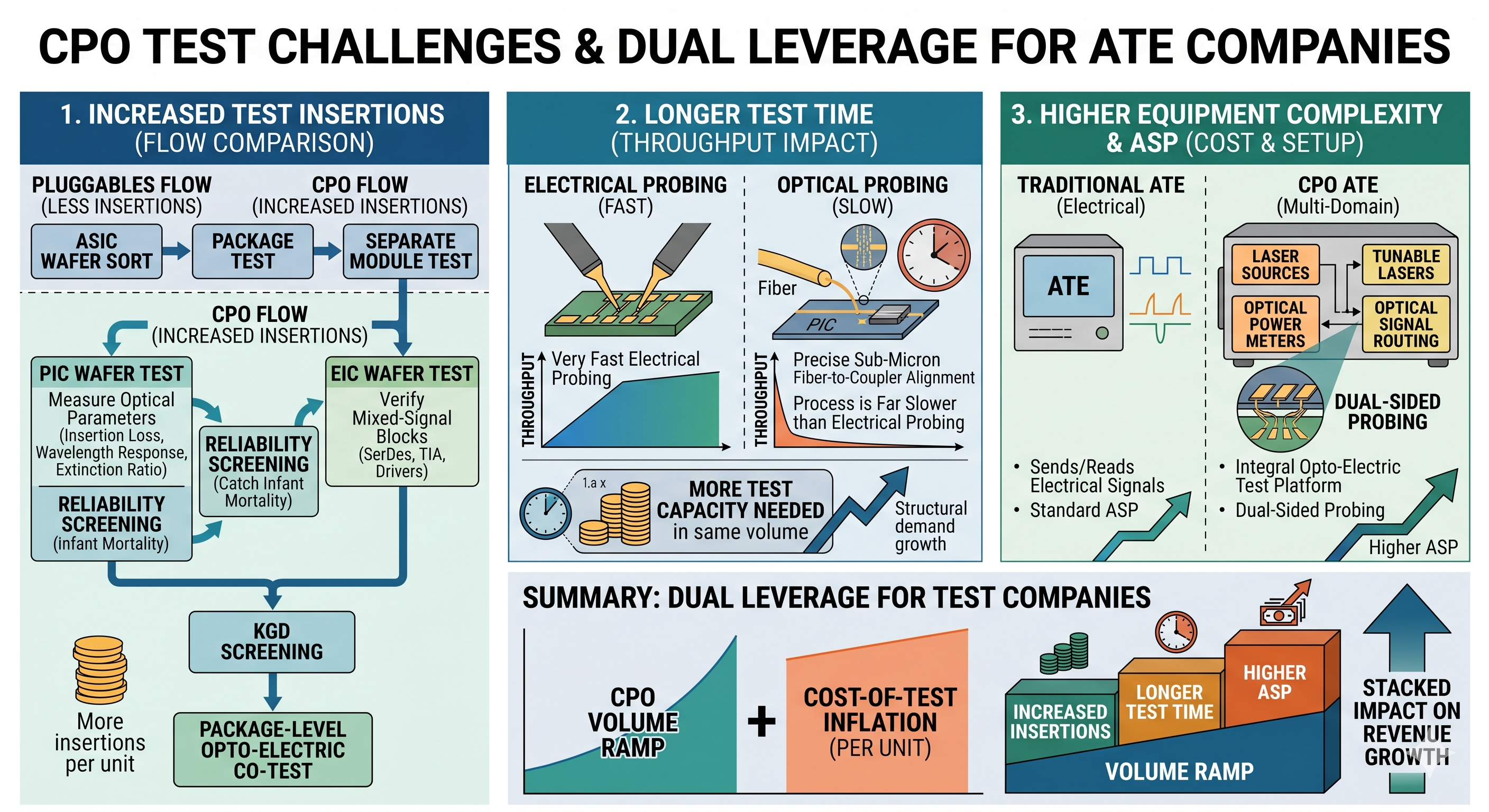
First, test insertions increase. With pluggables, you could separate the flow into ASIC wafer sort and package test, plus a separate module test. CPO requires PIC wafer test, EIC wafer test, KGD screening, and package-level opto-electric co-test.
PIC wafer test means measuring optical parameters like insertion loss, wavelength response, and modulator extinction ratio. On the EIC side, you need to verify mixed-signal blocks like SerDes, TIA, and drivers. On top of that, you add reliability screening to catch PIC infant mortality before packaging.
Second, test time gets longer. Electrical probing is very fast. But optical probing of a PIC requires precisely aligning a fiber to the coupler. Sub-micron alignment is needed, and this process is far slower than electrical probing. When throughput drops, you need more test capacity to process the same wafer volume. This is why test equipment demand can grow structurally even without an explosion in volume.
Third, equipment complexity and ASP go up. Traditional ATE sends and reads electrical signals. CPO requires integrating laser sources, tunable lasers, optical power meters, and optical signal routing into the test setup. Some architectures even require dual-sided probing, with electrical pads accessed from the top and optical couplers from the bottom. At that point, this is no longer a matter of bolting a few optical modules onto existing ATE. The test platform, probe interface, optical measurement, and automation flow all need to change.
The net result is that CPO creates dual leverage for test companies. It’s not just about CPO volume growing. The number of test insertions per unit increases, test time per unit gets longer, and equipment ASP goes up. You get per-unit cost-of-test inflation stacked on top of volume ramp.
This market has not yet hit a full-scale production explosion. That distinction matters. What’s opening right now is not the CPO volume market, but the CPO test infrastructure cycle. TSMC’s COUPE platform has been reported to be entering volume production in 2026, and Samsung Foundry has declared a CPO turnkey target for 2029.
NVIDIA announced Spectrum X and Quantum X photonics switches, officially committing to the photonic networking direction. As PIC wafers start coming out of foundries and CPO package flows take shape, the very first question is: what equipment, at what precision, and at what cost structure will be used to validate those PICs and packages?
That’s why equipment companies are moving first. Teradyne launched Photon 100 and acquired Quantifi Photonics. FormFactor acquired Keystone Photonics and is pushing the Triton test cell alongside Advantest and Tokyo Electron. Aehr has won SiPh WLBI customers and is positioning on the silicon photonics reliability side. Viavi, Santec, and Anritsu are all aligning their products and messaging toward 1.6T, 3.2T, and silicon photonics test.
In other words, this is not the point where CPO has already been deployed at scale. This is the point where equipment companies are shipping products, customer qualifications are starting, and early orders and design wins are accumulating. Actual large-scale deployment is likely post-2028. That’s exactly why the investment thesis right now is less about a CPO volume bet and more about an early-cycle bet on CPO test infrastructure getting built out.
Market perception has not fully caught up to this shift. Many investors still see Teradyne as a memory and SoC ATE company, Viavi as a telecom T&M company, and Aehr as a small-cap SiC burn-in name. But if CPO test opens up, the growth narrative for these companies could change meaningfully.
The customer structure is also different from the traditional ATE market. The usual semiconductor test customers are IDMs, foundries, and OSATs. In optical test, module makers and hyperscalers enter the picture. It’s not just Coherent, Lumentum, and Innolight; hyperscalers who are directly architecting their own optical interconnects also influence the test ecosystem.
The cycle is different too. SoC ATE demand is tied to GPU and ASIC ramps, but optical test demand moves with the pace of pluggable-to-NPO-to-CPO transitions. This timing can be offset from the traditional semiconductor test cycle by one to two years.
That’s why I don’t view optical test as a small subcategory of the existing ATE market. As CPO scales, test becomes its own investment cycle.
And that cycle is still in its early stages.
5 Bottlenecks in CPO Test
I’m re-dividing Layer 7 of the Optical Investment Map into 5 bottlenecks. This is not a simple equipment classification. The more important questions are:
Where does yield get stuck in the CPO production process? Where does test cost escalate? And which companies can convert that cost increase into revenue?
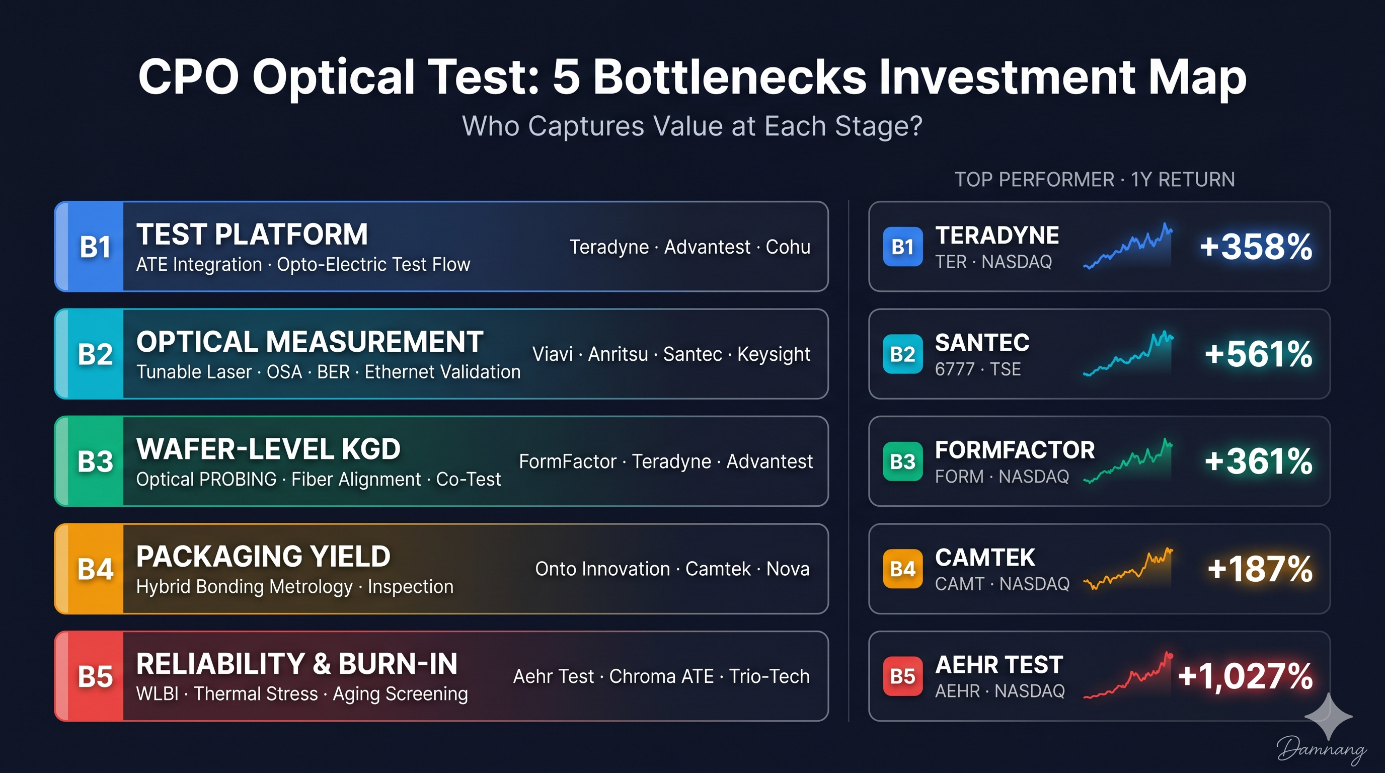
Bottleneck 1: Test Platform
Can CPO test be integrated into the existing electrical ATE flow?
In CPO, you cannot separate electrical and optical signals. At the wafer level, the optical engine level, the package level, and the module level, electrical test and optical test need to live within the same flow. So this is not about adding one piece of equipment. The test OS, handler, automation, test cell, and software flow all matter.
This bottleneck sits at the front end of the CPO infrastructure cycle. When foundries, OSATs, and hyperscalers prepare CPO lines or pilot production, the first thing they need is a production-ready test platform. That makes this the area most likely to generate revenue first when CPO capex opens up.
That said, this space is already dominated by large ATE incumbents. Companies like Teradyne and Advantest hold strong positions in SoC and memory test and are already capturing some AI test premium. CPO upside is real, but until CPO-specific revenue is visibly broken out, valuation risk needs to be weighed alongside it.
Relevant stocks: Teradyne (Photon 100, Quantifi Photonics acquisition, vertical integration strategy), Advantest (V93000-based open ecosystem), Cohu (supplementary exposure via handler, thermal, and automation)
Bottleneck 2: Optical Measurement
How fast and accurately can you generate, read, and analyze optical signals?
This includes tunable lasers, optical spectrum analyzers, BER testers, optical power meters, and Ethernet validation equipment. This bottleneck is not tied exclusively to CPO. It remains relevant across the 800G pluggable, 1.6T, and 3.2T optical transceiver cycle.
That makes Optical Measurement the most defensive bottleneck on this map. Even if CPO is delayed, revenue can hold up as long as optical data center speed upgrades continue. Conversely, if CPO accelerates, demand extends into SiPh wafer test, optical engine test, and package-level optical validation.
From an investment perspective, this is the area that reduces CPO timing risk. However, purity varies significantly by company. Santec has the highest optical test purity but carries valuation risk, Keysight has strong technical capabilities but optical exposure is diluted within the broader company, and Viavi sits in between as the most balanced candidate.
Relevant stocks: Viavi (optical production test and high-speed Ethernet validation), Anritsu (BERTWave-centric optical transceiver test), Santec (tunable laser and optical test pure-play character), Keysight (silicon photonics test system and broad T&M portfolio)
Bottleneck 3: Wafer-Level KGD
Can you secure Known Good Die at the PIC wafer level?
The scariest problem in CPO is a PIC defect discovered too late. If a PIC has already been integrated into an ASIC package when the problem surfaces, you may have to scrap the entire expensive switch ASIC package because of one bad PIC. That’s why securing optical KGD at the PIC wafer level before packaging becomes critical.
This process requires optical probing, electrical and optical co-test, fiber alignment, and in some cases dual-sided probing. You need to precisely align the fiber to the coupler and measure optical parameters like insertion loss, wavelength response, and modulator behavior at the wafer level.
From an investment perspective, this is the most structurally critical bottleneck for CPO yield. Probe cards and optical probing solutions in particular can take on recurring revenue characteristics as wafer volume grows.
However, this bottleneck doesn’t belong to FormFactor alone. The two ATE companies from Bottleneck 1 are reaching down into the KGD stage. Teradyne is pushing vertical integration from platform to wafer probing through its Photon 100 and dual-sided probing collaboration. Advantest covers optical KGD on top of V93000 through the Triton test cell, co-developed with FormFactor and Tokyo Electron. FormFactor holds an ATE-agnostic position that benefits regardless of which platform wins. That’s the key point.
And KGD has two dimensions: measurement-based screening (“does it meet optical spec?”) and stress-based screening (“will it survive over time?”). The former is this Bottleneck 3. The latter is the burn-in covered in Bottleneck 5. Aehr’s WLBI serves as the final gate in KGD.
Relevant stocks: FormFactor (Pharos optical probe, Keystone Photonics acquisition, Triton test cell, ATE-agnostic), Teradyne (Photon 100 + dual-sided probing), Advantest (Triton test cell for joint coverage with FormFactor)
Bottleneck 4: Packaging Yield and Bonding Metrology
Can PIC and EIC be reliably integrated inside the package?
This bottleneck is not a test layer that measures optical signals directly. But it is an adjacent bottleneck that drives CPO yield economics. To integrate PIC and EIC through hybrid bonding or advanced packaging flows, you need precise inspection of surface defects, bump alignment, bonding quality, and interconnect defects before and after bonding.
CPO packages are expensive. As more components are bundled together (switch ASIC, PIC, EIC, HBM or other chiplets), package value goes up. When yield loss occurs at this stage, it’s not a single-die problem; it’s a scrap problem for an entire high-value package.
From an investment perspective, these companies make money from the advanced packaging cycle before CPO, and CPO is more like an option layered on top. Onto, Camtek, and Nova already hold strong positions in HBM, 2.5D, 3D packaging, and hybrid bonding metrology. Financial quality is high, but the market does not view them as CPO test pure plays.
Relevant stocks: Onto Innovation (DragonFly G5, EchoScan, advanced packaging metrology), Camtek (Hawk, Eagle G5, surface defect inspection), Nova (WMC platform, dimensional and chemical metrology)
Bottleneck 5: Reliability and Burn-In
Can you screen out laser aging, wavelength drift, and early-life failure before production?
Optical devices behave differently from electrical logic. They are sensitive to time, heat, and optical power stress. Laser output can shift, wavelength can drift, and thermal tuning conditions can change. In CPO, the PIC is inside the package, making field replacement difficult when failures occur.
That’s why the importance of reliability screening rises as CPO approaches mass production. If demand grows for catching PIC early-life failures before packaging, wafer-level burn-in and package-level burn-in equipment gain significant value.
From an investment perspective, this is the most lagging bottleneck but potentially the highest-beta one. As CPO volume production draws closer, reliability and burn-in demand can be rapidly re-rated. Conversely, if CPO ramp is delayed, earnings conversion in this space gets pushed out too. So this area carries large upside and large timing risk simultaneously.
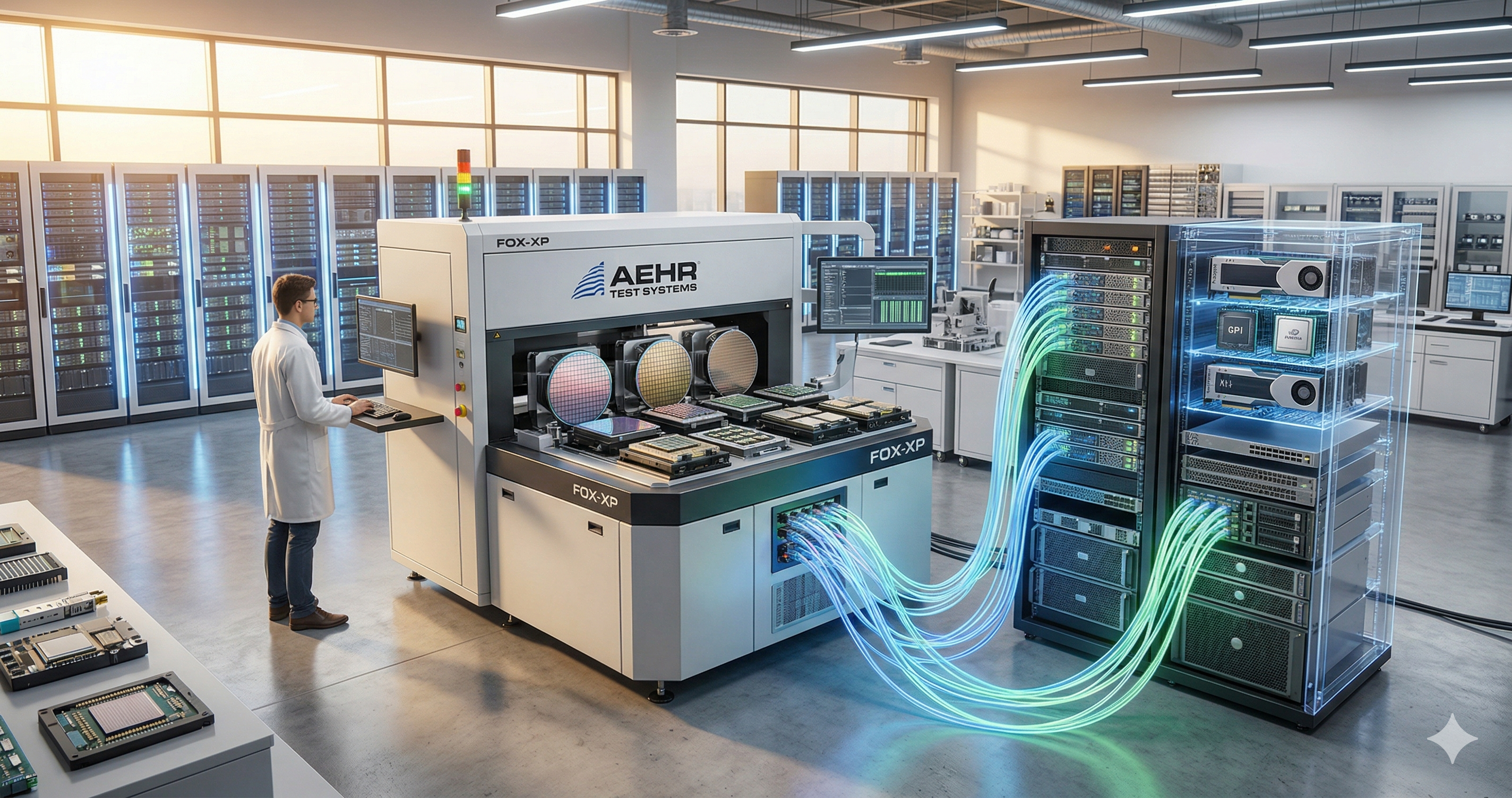
Relevant stocks: Aehr Test Systems (FOX XP-based wafer-level burn-in), Chroma ATE (PIC burn-in and Asian local ecosystem), Trio-Tech (burn-in board and burn-in service exposure)
Summary
That covers the structure of the CPO test value chain. The 5 bottlenecks show where yield gets stuck, where cost escalates, and which areas can generate revenue first.
But knowing the bottlenecks and picking stocks are two different things. Even within the same bottleneck, every company has a completely different profile. Some have high optical purity but already carry elevated expectations in their valuation. Some have deep technical advantages but no clear CPO-related orders yet. Some need CPO to arrive quickly, while others can make money from the pluggable cycle even if CPO is delayed.
So saying “CPO test is heating up” is not enough. What matters is which bottleneck opens first under the CPO adoption timeline you believe in, and which company can actually convert the economics of that bottleneck into revenue.
From here, I evaluate the 14 stocks across 6 investment Factors: optical theme exposure, CPO cost-of-test leverage, technical advantages, real orders and catalysts, financial quality, and valuation risk.
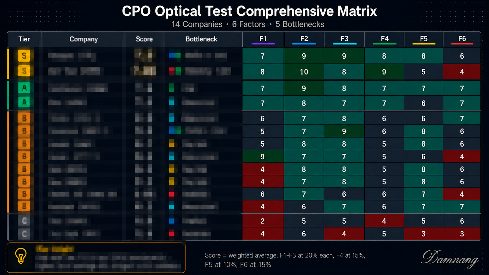
⚠️ 以上为公开免费部分。后续「14 只个股 × 6 因子」的逐一评估、评分矩阵与情景选股为付费内容,未包含。
本文引用的母图 —— Damnang《Optical Investment Map v1.0》(7 层价值链,Test = Layer 7)已单独整理。
关联文章:
第二部分:解析(深度解读)
文章核心论点摘要
- 核心投资机会:当前最值得关注的半导体投资赛道并非 CPO(共封装光学)的大规模量产本身,而是支撑其量产所必需的测试基础设施。这个”卖铲子”的阶段正处于早期,市场认知尚未充分反映其价值。
- 核心逻辑:CPO 将光引擎(PIC)与电芯片(ASIC)封装在一起,这从根本上改变了测试的经济学。测试次数增加、单次测试时间变长、测试设备复杂度(单价)提升,形成了测试成本的”双重杠杆”效应,为测试设备公司创造了结构性增长机会。
- 核心策略:投资的关键在于识别 CPO 测试价值链中的5 大瓶颈,并根据不同的 CPO 落地情景,选择能在对应瓶颈中率先将成本转化为收入的标的。文章重点分析了 14 只相关股票,但核心是提供一套分析框架。
关键概念解读
- CPO (共封装光学):把负责光信号收发的”光引擎”(PIC)和负责计算的”大脑”(ASIC 芯片)封装在同一个底座上,距离极近。这能大幅提升带宽、降低功耗,是未来 AI 数据中心互联的终极方案。
- PIC (光子集成电路):可以理解为”光芯片”,它处理的是光信号,比如产生、调制、探测光。就像电子芯片(EIC)处理电信号一样。
- KGD (已知良好芯片):在将芯片(尤其是昂贵的 PIC)封装进最终产品前,先进行严格测试,确保它是”良品”。在 CPO 中,如果封装后才发现 PIC 是坏的,整个昂贵的封装体(包括 ASIC)可能都要报废,所以 KGD 至关重要。
- WLBI (晶圆级老化测试):在芯片还是一片晶圆(未切割)时,就对其进行高温、高压等加速老化测试,以筛选出早期失效的芯片。这是确保 CPO 可靠性的关键一步。
- ATE (自动测试设备):用于自动化测试半导体芯片的”大机器”,可以理解为芯片的”体检中心”。传统 ATE 主要测电信号,而 CPO 测试需要能同时测光和电信号的”光-电一体” ATE。
5 大瓶颈逐一解读
| 瓶颈 | 核心逻辑 | 为什么是瓶颈? | 投资意义 |
|---|---|---|---|
| 1. 测试平台 | 能否将光测试无缝集成到现有的电测试流程中? | CPO 要求光、电信号在同一流程中测试,需要全新的测试平台、操作系统和自动化软件,而非简单”加个模块”。这是 CPO 产线建设的第一道门槛。 | 最先受益。当晶圆厂、封测厂开始建设 CPO 产线时,最先采购的就是这个平台。但市场由 Teradyne、Advantest 等巨头主导,CPO 业务占比尚小。 |
| 2. 光学测量 | 如何快速、精准地产生、读取和分析光信号? | 需要可调谐激光器、光谱仪、误码仪等精密仪器。这个瓶颈不依赖 CPO,800G/1.6T 光模块升级同样需要。 | 最”防御性”。即使 CPO 延迟,数据中心速率升级也能支撑其收入。是降低 CPO 投资”时间风险”的避风港。 |
| 3. 晶圆级 KGD | 如何在 PIC 晶圆阶段就确保它是”已知良好芯片”? | 这是 CPO 良率的结构性瓶颈。需要在晶圆级对 PIC 进行光、电联合探测,涉及亚微米级光纤对准,速度远慢于电测。一旦漏测,封装后报废成本极高。 | 最关键的良率瓶颈。探针卡和光探测方案具有”耗材”属性,随晶圆量增长而持续产生收入。FormFactor 是核心玩家。 |
| 4. 封装良率与键合计量 | 如何确保 PIC 和 EIC 在封装内被可靠地集成在一起? | CPO 封装价值极高,键合过程中的任何缺陷(如对准偏差、空洞)都会导致整个封装体报废。这需要高精度的检测设备。 | “期权”属性。这些公司(如 Onto、Camtek)主要受益于 HBM 等先进封装周期,CPO 是锦上添花的额外增长点。 |
| 5. 可靠性与老化 | 如何在大规模生产前,筛选出激光器老化、波长漂移等早期失效? | 光器件对热和应力敏感,一旦封装后失效,现场更换极其困难。因此,量产前的老化筛选(如 WLBI)变得至关重要。 | 最”滞后”但”高 β”。CPO 真正放量时,需求会急剧爆发。但如果 CPO 延迟,业绩兑现也会推迟,时机风险最大。 |
投资逻辑梳理
为什么光测试是当前值得关注的赛道?
- 结构性增长:CPO 带来了测试次数、测试时间、设备单价的”三重增长”,而非简单的量增。这是测试成本的结构性膨胀。
- 早期周期:当前(2026 年)是 CPO 测试基础设施的建设期,而非 CPO 大规模量产期。设备公司正在出货、客户认证、积累早期订单。市场尚未充分认识到这个”卖铲子”阶段的投资价值。
- 客户结构变化:除了传统的芯片厂和封测厂,光模块厂商和直接设计光互联的云巨头(Hyperscaler)也进入了测试设备的客户名单,拓宽了市场空间。
CPO 测试的”双重杠杆”效应
- 第一重杠杆:量增。CPO 出货量增长,直接带动测试设备需求。
- 第二重杠杆:价增。每个 CPO 单元所需的测试次数更多、测试时间更长、测试设备更复杂(单价更高),导致单位测试成本上升。这意味着即使出货量不变,测试设备的总市场空间也在扩大。
关键时间节点和催化剂
- TSMC COUPE (2026 年):台积电的 COUPE 平台(一种 CPO 技术)据报道将在 2026 年进入量产。这是最直接的催化剂,标志着 CPO 从研发走向小批量生产,将直接拉动测试设备订单。
- NVIDIA Spectrum X / Quantum X (已发布):英伟达正式发布光交换网络方案,表明其坚定拥抱光子网络方向。这为整个 CPO 产业链提供了最强的需求背书。
- Samsung Foundry CPO Turnkey (2029 年):三星代工宣布其 CPO 交钥匙服务目标在 2029 年。这代表了更远期的量产预期,为长期投资提供了时间锚点。
- 设备公司产品发布与收购:Teradyne 推出 Photon 100、收购 Quantifi Photonics;FormFactor 收购 Keystone Photonics 等。这些是行业正在”动起来”的直接证据,表明头部公司正在积极布局。
风险提示
- 技术路线风险:CPO 技术路径(如 TSMC COUPE、Intel、Broadcom 等)尚未完全统一,不同路径对测试的要求可能不同,导致部分设备公司押错方向。
- 量产时间不及预期:CPO 的大规模量产(Post-2028)仍存在不确定性。如果技术瓶颈或成本问题导致量产一再推迟,那么依赖 CPO 放量的公司(如 Aehr)将面临业绩和估值的双重压力。
- 估值风险:部分公司(如 Santec)虽然光测试纯度最高,但市场已给予较高预期,股价可能已提前反映部分利好。一旦催化剂落空,回调风险较大。
- 竞争格局恶化:传统 ATE 巨头(Teradyne, Advantest)实力雄厚,新进入者或小公司可能面临激烈的价格战和客户争夺。
- 地缘政治风险:半导体设备和测试设备是中美科技竞争的核心领域,出口管制和供应链脱钩可能影响相关公司的客户获取和业务开展。
本文仅供学习交流,不构成投资建议。原文版权归原作者所有。