Damnang's Optical Investment Map v1.0 — 光投资全产业链地图:7 层价值链与 50 只标的
整理自 Damnang:把光投资拆成 7 层价值链(材料/器件/连接 IC/PIC 平台/代工/封装/测试),叠加 FRO→LPO→NPO→CPO 架构演进轴,并梳理 50 只相关标的与垂直整合关系。英文原文 + 中文解读。
本文整理自 Damnang (Substack) 的科技投资分析文章,原文发布于 2026-04-20(内容截至 2026-04-17)。 结构为 正文(英文原文)+ 解析(中文深度解读),方便中英对照阅读。
第一部分:正文(Original Article)
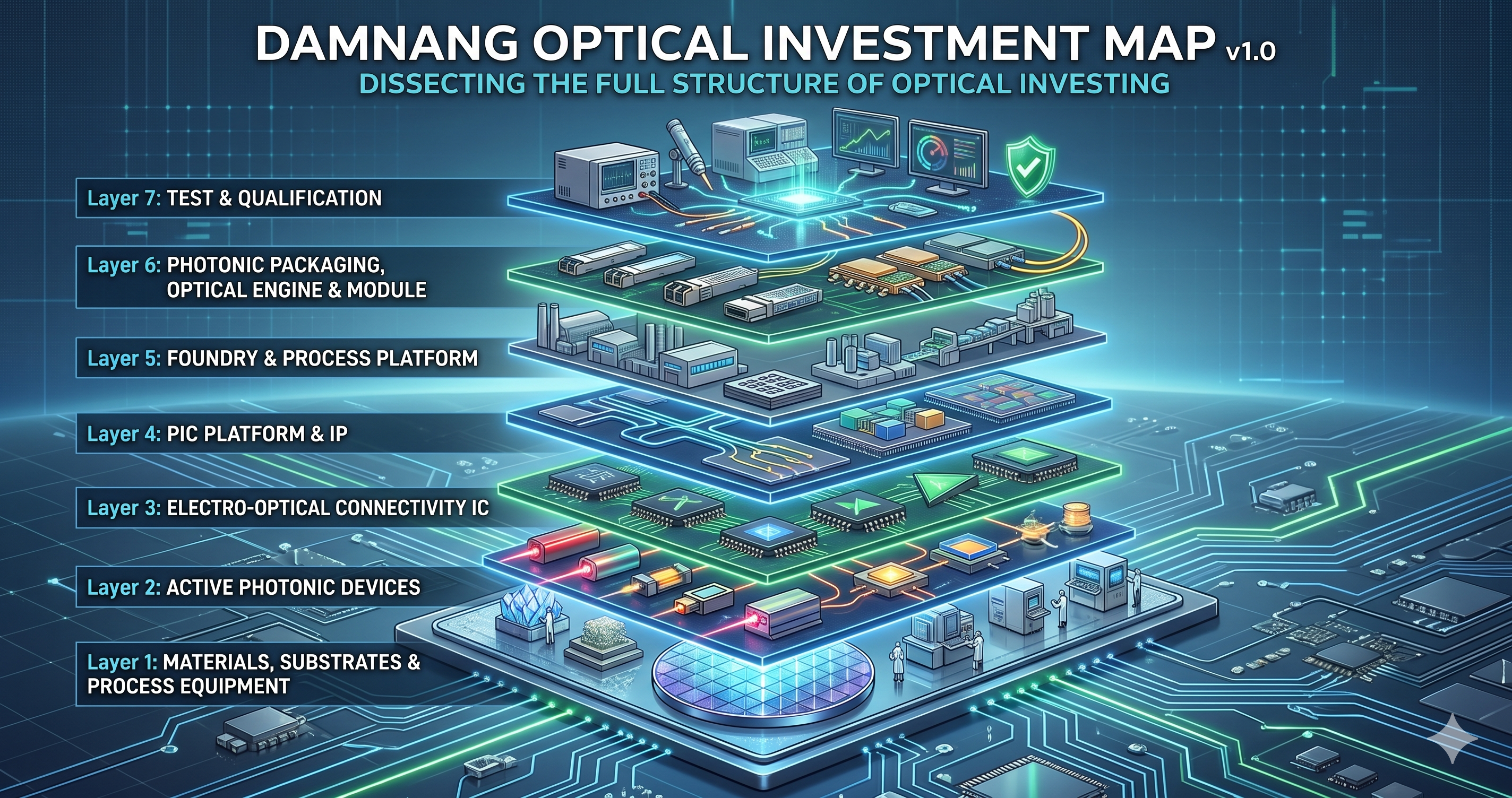
Damnang’s Optical Investment Map v1.0
Dissecting the Full Structure of Optical Investing Across 7 Layers and 50 Tickers
来源:Damnang (Substack) · 2026-04-20
These days the market is drowning in words like optical, silicon photonics, and CPO. But most investors know the keywords without actually seeing the full picture of the value chain behind them.
Some people look at Coherent and Lumentum and think they understand optics. Others hear CPO is the future and go hunting for related stocks. But optics is not a theme that ends at a handful of laser names. It is a value chain that tangles together materials, photonic devices, connectivity ICs, PIC platforms, foundries, packaging, modules, and test. Which layer you look at completely changes the risk profile and the return structure.
This piece is a map built to show that whole picture in one shot.
I’ve split the optical value chain into seven layers, overlaid the architecture evolution axis (FRO, LRO, LPO, NPO, CPO), and organized each company by where it sits in that structure.
This time I’m going one step further.
Over the past twelve months, optical-related stocks have run anywhere from +200% to +1,700%. Readers keep asking the same things.
Is it too late to get in?
What should I be watching?
I’m answering those questions head-on in a paid-subscriber section that covers cycle diagnosis, the next five years’ game-changers, and a scoring matrix that rates 22 names across 9 factors. The scoring methodology is fully disclosed, so you can re-weight it yourself.
This map isn’t going to be perfect. I might miss names or layers worth adding. If you spot something while reading, drop it in the comments and I’ll update as I go.
The 7-Layer Value Chain
All 52-week returns in the tables below are estimates versus one year ago as of April 17, 2026.
Layer 1: Materials, Substrates & Process Equipment
The raw materials for optical devices, plus the core equipment that processes them.
InP / III-V Epitaxy / MOCVD. The raw-material family for laser chips. Epitaxial films are grown on InP substrates to build laser wafers. Three things are involved: substrate manufacturing, epi growth, and MOCVD equipment.
SOI Wafer. The substrate for silicon photonics (SiPh). Every time SiPh foundry capacity expands, SOI wafer demand scales alongside it.
Next-Gen Modulator Materials. TFLN and EO polymer. Both offer higher modulation efficiency than silicon MZM but are still early and unvalidated at volume. TFLN is starting to see volume production in China (Liobate, AFR, and others).
TFLN-based PIC designers and foundries (QCi, HyperLight) are covered in L4 and L5.
This layer is won on supply bottleneck and manufacturing difficulty. It is the first layer to reflect the early capex cycle of the AI optical buildout.
Layer 2: Active Photonic Devices
The pure photonic-device layer. The things that create light (lasers), modulate light (modulators), and detect light (photodetectors).
2A Laser Sources. DFB, EML, VCSEL, CW lasers. The single most important bottleneck in the whole value chain.
Industry checks say 200G/lane EML supply is tight, and CPO brings another wave of demand for external light source (ELS) CW lasers.
Japanese majors like Sumitomo Electric and Mitsubishi Electric also supply EMLs, but those are business units inside conglomerates and hard to classify as pure plays.
2B Modulators. The device that rides data onto light. Silicon MZM is mainstream. TFLN and EO polymer are the challengers. Most of them get integrated into PICs (L4) or modules (L6), so very few trade as standalone names. LWLG’s EO polymer (L1) also hits this layer as a modulator material. Chinese TFLN modulator makers like Liobate and AFR have started volume production, but they are still early and mostly private.
2C Photodetectors. The device that converts light back into an electrical signal. Almost all of them sit inside PICs, so there are no meaningful standalone names.
This layer has the deepest technical moat. For lasers in particular, the supplier pool is narrow enough that pricing power moves directly with the supply-demand balance.
Layer 3: Electro-Optical Connectivity IC
Electrical semiconductors that bridge the photonic devices (L2) and the digital system. TIAs, modulator drivers, DSPs, SerDes, and retimers all live here.
These sit inside optical modules, but fundamentally they handle electrical signals, not light.
The faster the line rate, the harder this IC becomes.
Going from 400G to 800G to 1.6T, analog performance requirements explode, and the list of companies that can actually build these chips is short.
You can swap module vendors and still end up with the same company’s IC inside.
Layer 4: PIC Platform & IP
This is not just PIC design. It is the platform layer that includes optical integration IP, coupling technology, photonic fabric, and other forms of system-level photonics enablement.
The core story here is the M&A war.
Marvell bought Celestial AI.
Credo bought DustPhotonics.
Astera Labs bought aiXscale.
AMD bought Enosemi.
All in 2025-2026. The pure-play optical PIC names that have not been acquired yet could be the next targets.
There are not many public pure plays in this layer, so the right lens right now is M&A premium.
Private chokepoints: Ayar Labs, Lightmatter, HyperLight, nEye Systems. The IPOs or acquisitions of these companies will be the catalysts for the listed names.
Layer 5: Foundry & Process Platform
The manufacturing layer that takes PIC and photonic-device wafer production on contract. SiPh demand has surged to the point where capacity has become the bottleneck.
Tower Semiconductor is the main supplier. GlobalFoundries and UMC are pushing in.
TSMC also offers a SiPh COUPE platform and SoIC advanced packaging for CPO, but its revenue share is tiny relative to the total company, so it is hard to treat as a pure photonics play.
Samsung Foundry is also developing SiPh processes, a variable that could reshape the competitive landscape of this layer down the road.
On the specialty side, QCi operates the first U.S. TFLN-only foundry, in Tempe AZ.
The company that puts capex in first locks in customers. Strategic value is high enough that foundries are suing each other over patents.
Layer 6: Photonic Packaging, Optical Engine & Module
The layer that packages and assembles PIC die into final form. This is the highest-revenue-volume layer in the chain, and at the same time, architecture-transition positioning here will decide the next two to three years of returns.
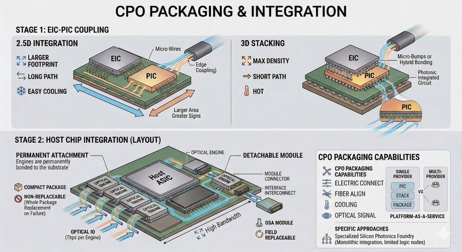
Layer 6-A: Optical Engine & Module. Within this sub-layer, architecture is evolving, and that evolution is also the investment timeline.
- FRO (Fully Retimed Optics). Transceivers with integrated DSP plus retimer. Most optical module revenue right now comes out of this architecture.
- LRO (Linear Retimed Optics). Retiming kept, DSP replaced with a linear driver. The middle step between FRO and LPO.
- LPO (Linear Pluggable Optics). Retimer removed entirely. 30-50% power savings. L3 analog IC performance determines the module’s overall behavior.
- NPO (Near-Packaged Optics). Optical engine placed on the switch board but still in a separate package.
- CPO (Co-Packaged Optics). Optical engine 3D-bonded into the same package as the ASIC. Important, but right now this is a section where option value comes before revenue.
Layer 6-B: Deployment Infrastructure. The physical path light actually travels through. Optical fiber, cable, connectors. Whether the architecture is FRO or CPO, every transceiver shipped ships with fiber and connectors alongside. Architecture-agnostic beneficiaries.
Layer 6-C: Optical Transport Systems. Long-haul data-center interconnect (DCI) and telecom metro network equipment. Different economics than deployment infra.
Layer 7: Test & Qualification
The layer that validates performance at every step: devices, modules, and systems. Test complexity ramps sharply with line rate. In the CPO era, wafer-level test and burn-in become even more important.
Whichever architecture wins, whichever transceiver company wins, the test gear is unavoidable. A structure that rides market growth without taking on technology risk.
Vertical Integration Cross-Reference
This section collects the companies that span two or more layers.
Vertical integration is a structural-moat indicator. Tying multiple layers inside a single company reduces upstream supply risk, stacks margins across layers, and deepens customer lock-in.
That said, vertical-integration depth does not automatically translate into stock performance. In the current cycle, it’s actually the opposite in places. I’ll come back to that at the end of the section.
Positions count the dots in the matrix.
L6 gets counted as separate positions because the sub-layers (6A/6B/6C) are genuinely different businesses.
Directions of Vertical Integration
- Upstream integration (L1 or L2 → L6). Starting from L1 materials or L2 devices and reaching down to L6 modules. Coherent, Lumentum, AAOI, and Sumitomo are the archetypes. Most are decades-old optical-communications natives.
- Downstream integration (L3 → L4 → L6). Starting from L3 ICs and expanding into L4 PIC and L6 modules through M&A. Cisco, Credo, and Marvell fit this. All relatively recent arrivals in optical communications.
- Materials-devices integration (L1 + L2). The two core upstream layers only. IPG, Sivers, Yuanjie, nLIGHT, Aeluma, LWLG. The common thread is owning their own wafer fab.
- IC-laser integration (L2 + L3). Analog IC companies that also own their own laser chip. MACOM and Semtech. A real differentiator in today’s EML shortage.
- Middle integration (L4 + L6). PIC design and module manufacturing bundled together. POET, Innolight, Eoptolink. Fab-lite plus in-house PIC design.
- Specialty integration. QCi (L4 + L5, own PIC plus TFLN foundry). Ciena (L6-A + L6-C, engine plus transport).
What we’ve done up to this point is the structural map of the optical value chain. 50 names, which layer they play in, which role they play, and how 22 vertically integrated companies connect across the map. But what investors actually want to know isn’t the map. It’s what comes next.
- The sector is already up more than +1,000%. Is it still investable?
- Which inning is this cycle in? Will this turn into the 2001 dotcom optical crash?
⚠️ 以上为公开免费部分(7 层结构 + 垂直整合交叉参照)。后续「周期诊断、未来五年变革方向、22 名 × 9 因子评分矩阵」为付费内容,未包含。
第二部分:解析(深度解读)
文章核心论点摘要
- 产业链全景,而非单点主题:光投资不是”几个激光器名字”那么简单,而是横跨材料、光子器件、连接 IC、PIC 平台、代工、封装、测试 7 层 的完整价值链。你盯着哪一层,风险收益结构就完全不同。
- 架构演进轴决定时间窗口:FRO → LRO → LPO → NPO → CPO,光引擎越靠近 ASIC,功耗与带宽密度越好;但 CPO 当前仍是”期权价值 > 营收”,真正放量在更远期。
- 垂直整合是结构性护城河指标:跨层整合能降低上游供应风险、跨层堆叠毛利、加深客户锁定;但当前周期里,整合深度未必直接转化为股价表现,甚至可能出现”整合反而拖累”的情况。
- 研究方法而非荐股:作者把 50 只标的按所在层与角色归类,并标出 22 家跨层垂直整合公司;真正的”周期诊断 + 未来五年变革 + 22 名 × 9 因子评分矩阵”在付费段,本文不含。
关键概念解读
- CPO / LPO / NPO / FRO / LRO:光模块到光引擎的架构演进轴。FRO 含完整 DSP+retimer;LPO 去掉 retimer,省 30–50% 功耗但更依赖 L3 模拟 IC;NPO 光引擎仍在独立封装;CPO 把光引擎 3D 键合进 ASIC 同封装。
- PIC(光子集成电路):处理光信号的”光芯片”,由波导、调制器、探测器等集成。
- EML / CW Laser(外置光源):激光器是整条价值链最重要的瓶颈;200G/lane EML 供给紧张,CPO 又带来 ELS CW 激光器的新增需求。
- TFLN / EO Polymer(薄膜铌酸锂 / 电光聚合物):下一代调制器材料,调制效率高于硅 MZM,但仍早期、未规模验证。
- SiPh(硅光)/ SOI 晶圆:硅光路线依赖 SOI 衬底,代工产能扩张直接拉动 SOI 需求。
- MOCVD / InP 外延:在 InP 衬底上生长激光器外延片的核心工艺与设备。
- Vertical Integration(垂直整合):一家公司横跨多层(如 L1+L2、L3→L6),既是护城河也是潜在负担。
7 层价值链逐层拆解
| 层 | 核心内容 | 投资要点 / 代表玩家 |
|---|---|---|
| L1 材料 / 衬底 / 工艺设备 | InP 外延、MOCVD、SOI 晶圆、TFLN/EO 聚合物 | 赢在供应瓶颈与制造难度,最先反映 AI 光建设早期 capex 周期。 |
| L2 有源光子器件 | 激光器(2A)、调制器(2B)、探测器(2C) | 技术护城河最深;激光器供应商池最窄,定价权随供需走。EML 短缺是核心矛盾。 |
| L3 光电连接 IC | TIA、调制驱动器、DSP、SerDes、retimer | 线速率越高越难做,能做的公司极少;换模块厂可能还是同一家 IC。 |
| L4 PIC 平台与 IP | PIC 设计 + 集成 IP / 耦合 / 光子 fabric | 核心故事是 并购战(Marvell/Credo/Astera/AMD 2025–26 连续收购);公开纯 play 少,看 M&A 溢价。私有 chokepoints:Ayar Labs、Lightmatter、HyperLight、nEye。 |
| L5 代工与工艺平台 | SiPh 晶圆代工、COUPE/SoIC 先进封装 | Tower 主供,GF/UMC 推进;TSMC 占营收极小难称纯光标的;Samsung 在开发;QCi 运营美国首个 TFLN 专属代工。先投 capex 者锁定客户。 |
| L6 光子封装 / 光引擎 / 模块 | 6A 光引擎与模块、6B 部署基础设施(光纤/连接器)、6C 光传输系统 | 链中营收体量最大;架构演进定位决定未来 2–3 年回报(见下)。架构无关受益者在 6B。 |
| L7 测试与认证 | 器件/模块/系统各级验证,晶圆级测试与老化 | 无论哪种架构赢、哪家模块厂赢,测试设备都绕不开——搭市场增长顺风且不承担技术路线风险。 |
架构演进轴(Layer 6-A)的投资含义
| 架构 | 特征 | 当前状态 |
|---|---|---|
| FRO | 含 DSP + retimer 的全重定时光模块 | 当前大多数模块营收来源 |
| LRO | 保留重定时,DSP 换线性驱动器 | FRO 与 LPO 的中间态 |
| NPO | 光引擎上交换机板,仍在独立封装 | 过渡形态 |
| LPO | 去掉 retimer,省 30–50% 功耗 | 性能由 L3 模拟 IC 决定 |
| CPO | 光引擎 3D 键合进 ASIC 同封装 | 重要,但当前期权价值 > 营收 |
垂直整合方向一览
- 上游整合 (L1/L2 → L6):Coherent、Lumentum、AAOI、Sumitomo(光通信老牌原生玩家)。
- 下游整合 (L3 → L4 → L6):Cisco、Credo、Marvell(近期通过并购入局)。
- 材料–器件整合 (L1+L2):IPG、Sivers、Yuanjie、nLIGHT、Aeluma、LWLG(共同点是自有晶圆厂)。
- IC–激光整合 (L2+L3):MACOM、Semtech(EML 短缺下的真实差异化)。
- 中间整合 (L4+L6):POET、Innolight、Eoptolink(fab-lite + 自研 PIC)。
- 特色整合:QCi(L4+L5 自有 PIC + TFLN 代工)、Ciena(L6-A + L6-C 引擎 + 传输)。
投资逻辑梳理
- 别只盯激光器名字,要看价值链位置:同一只”光股票”,落在 L2 还是 L6,风险收益结构完全不同。
- 架构演进节奏决定时间窗口:CPO 当前是期权价值 > 营收,但 L6 的架构定位、L7 的测试刚需,决定了未来 2–3 年的回报归属。
- 垂直整合是护城河,也可能是负担:当前周期里整合深度并不自动等于股价表现,需结合估值与整合质量判断。
- 盯紧并购催化剂:未上市的纯 PIC chokepoints(Ayar Labs 等)一旦 IPO 或被收购,就是上市关联标的的催化事件。
- 代工产能是瓶颈:谁先投 capex 谁先锁定客户,战略价值高到代工厂之间为专利互诉。
关键时间节点与催化剂
- 并购战持续:2025–2026 年 Marvell / Credo / Astera Labs / AMD 连续收购,未上市纯 PIC 标的的 IPO/收购是后续催化。
- TSMC COUPE 进入 CPO 量产(2026):标志硅光代工产能从研发走向小批量。
- Samsung Foundry SiPh 进程:可能重塑 L5 代工竞争格局的变量。
- LPO / CPO 渗透节奏:决定 L3 模拟 IC、L6 封装与 L7 测试的需求时序。
风险提示
- 估值风险:板块过去 12 个月已涨 +200% 至 +1,700%,部分标的预期已大幅透支。
- 技术路径风险:FRO/LPO/NPO/CPO 架构尚未定局,押错路线方向的标的会被淘汰或压制。
- 周期风险:板块已涨超 +1,000%,是否重演 2001 年光通信崩盘,作者本人也将其列为开放问题。
- 地缘政治 / 供应链风险:半导体设备与光器件是中美科技竞争核心领域,出口管制与脱钩可能影响客户获取。
- 内容边界:本文仅为公开免费的结构图部分;「周期诊断、未来五年变革、22 名 × 9 因子评分矩阵」为付费内容,未包含,不构成完整投资结论。
本文仅供学习交流,不构成投资建议。原文版权归原作者所有。