A Comprehensive Overview of High-Speed Optical Communications — 高速光通信全景:从 IM-DD、VCSEL 到硅光与相干光学
整理自 chadw(Silicon Code Design, Substack)的技术科普:从短距主力 IM-DD、VCSEL 激光器、光纤模色散与接收端 PIN/TIA,到底层缩放三轴与四大技术趋势(共封装光学/硅光/外调制/相干光学)。英文原文 + 中文解读。
本文整理自 chadw (Substack / siliconcodesign.com) 的技术科普文章,原文发布于 2026-04-14。 结构为 正文(英文原文)+ 解析(中文深度解读),方便中英对照阅读。 ⚠️ 文末四大技术趋势(CPO / 硅光 / 外调制 / 相干光学)的详细展开在付费段,公开免费部分仅列出名称与一句话定位,本文如实标注、未含付费深解。
第一部分:正文(Original Article)
A Comprehensive Overview of High-Speed Optical Communications
来源:chadw (Substack) · 2026-04-14
In this post I will cover entire optical communications space:
I will introduce the conventional IM-DD optical approach with VCSELs used for short reach
I will then highlight challenges with scaling conventional IM-DD to higher data rates
Then I’ll explain techniques to improve data bandwidth:
🔒 Co-packaged optics
🔒 Silicon photonics
🔒 External modulation
🔒 Coherent optics
High speed optical interconnects have become one of the hottest markets in AI data centers. As bandwidth demand rises, the challenge is no longer just computing on data faster, but moving it across packages, boards, racks, and clusters efficiently.
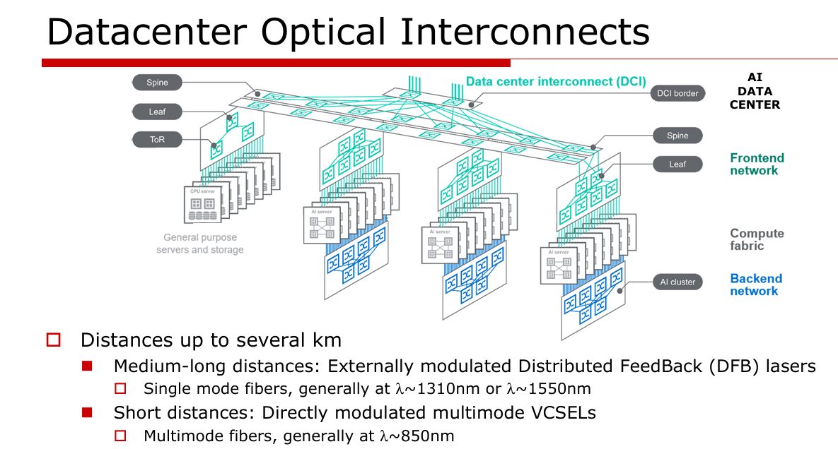
Figure 1. An Architecture of a Data center with scale up and scale out networks and how optical plays a role in both short reach and long reach communications. Source: Temporiti, E. “VCSEL-based Solutions: Components, Circuits and Integration” ISSCC 2026
The optical space has exploded over the past few years with many companies and startups proposing solutions to tackle data demands.
But I want to step back and ask ourselves: what are the first principles challenges with scaling high-speed optical communications?
The workhorse for short reach optical communications today are IM-DD with pluggable optical transceivers. Lets take a looks at what each consists of.
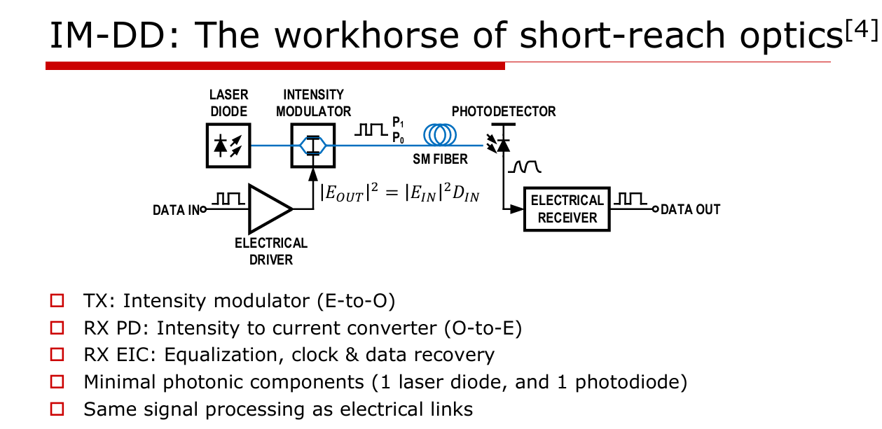
Figure 2. A high level block diagram of an IM-DD system. Source: P. Hanumolu. “Analog and Mixed-Signal Approaches for Low-Complexity Coherent Optical Links” ISSCC 2026
IM-DD is the workhorse of short reach optics. IM-DD encodes information in optical intensity (whether that be 0/1 or higher levels in PAM4) and recovers it through direct detection.
This intensity modulation can be performed in one of two ways:
Direct modulation - the laser is turned up/down by the electrical signal
External modulation - a driver modulates a steady optical carrier
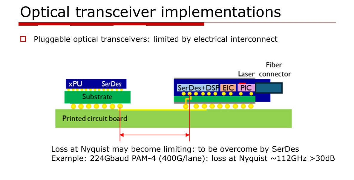
Figure 3. A conventional Pluggable optical transceiver module highlighting the problem of electrical interconnect at higher data speeds. Source: P. Ossieur. “Introduction to Optical Communication Systems From VCSELs, integrated photonics to coherent solutions” ISSCC 2026
These IM-DD are typically packaged into pluggable optical transceiver modules that sit far away from the chip. These are match-box sized modules that take in electrical (client) side data and convert it to optical (line side). Each block consists of following:
Serdes + DSP - For serializing / desterilizing the data from/to host and perform equalization
EIC - Electrical integrated circuit - consists of the electrical circuits fabricated in electrical processes (drivers, mixed signal conditioning, etc)
PIC - Photonic integrated Circuit - consists of the optical circuits fabricated in optical processes (Si Photonics, VCSELs, etc)
Optical transceiver modules are a very mature technology that has scaled in data throughput for many years. However, with AI workloads demanding 224+ GPBS throughput capability, the performance of the optical transceiver itself needs to adapt, as well as the signal integrity between host die and optical engine.
Next I will break down the architecture of an IM-DD in each of its components:
Transmitter
Fiber
Receiver
I will discuss several options for each and important design considerations.
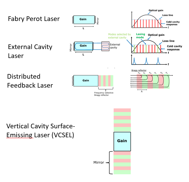
Figure 4. A progression of lasers from textbook Fabry-Perot lasers to Modern VCSEL lasers with Bragg reflectors. Source: F. Aflatouni. “Silicon photonics-based solutions: components, circuits, and integration” ISSCC 2026
Lasers are powered by a large pump current stimulating emission. Photons with energy close to the material bandgap interact with electron - hole pairs and cause identical photons to be emitted. This causes an “optical gain” of photons within the active region.
This photons is then confined using two mirrors: one opaque, and other that is semitransparent to allow the light to shine through.
Lasing occurs when the pump current is high enough such that optical gain > optical losses.
Then, either a cavity structure or frequency selective bragg reflectors selects which optical modes are sustained.
In a Distributed Feedback laser (DFB) laser, a periodic grating of Bragg reflectors provides wavelength - selective optical feedback, favoring a narrow lasing wavelength. These Bragg Reflectors are highly tunable depending on the index of refractions and the lengths and # of sections.
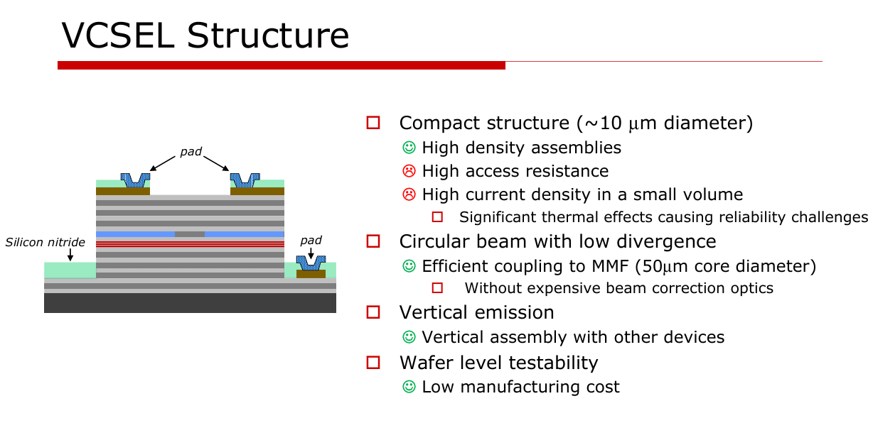
Figure 5. A cross section of a VCSEL. Source: E. Temporiti. “VCSEL-based Solutions: Components, Circuits and Integration” ISSCC 2026
VCSELS are lasers that emit light vertically in a circular cross section. The active region consists of multiple quantum wells that enhances optical gain. Distributed bragg reflectors are stacked on the top and bottom of the active region with alternating refractive indexes. These layers are fabricated using epitaxial growth on a substrate.
The light is then confined with an oxide and current is pumped in through pads. The light is shown vertically above and redirected toward the optical fiber with optics.
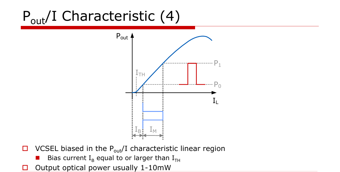
Figure 6. The Pout / I Characteristic of a VCSEL and the region of switching. Source: E. Temporiti. “VCSEL-based Solutions: Components, Circuits and Integration” ISSCC 2026
The Pout/I of VCSELs almost resembles a linear diode. The VCSEL begins lasing above a particular threshold current and exhibit a linear relationship between Pout / Iin over a useful operating region. Lasers require a DC bias to set the device in the linear region.
One important parameter is the extinction ratio, which is the ratio between P1 and P0. A higher extinction ratio is preferred as it improves BER margin to detect teh signal at the other end, but higher extinction ratios require higher currents, and therefore power, to drive the device.
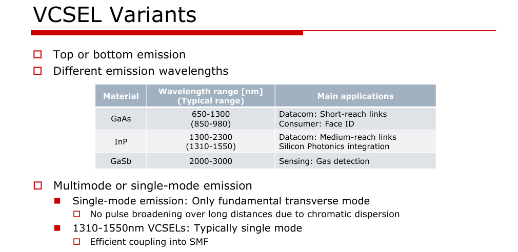
Figure 7. VCSEL material variants. Source: E. Temporiti. “VCSEL-based Solutions: Components, Circuits and Integration” ISSCC 2026
The two major materials used in lasers are GaAs or InP:
850 nm GaAs VCSELs are common for short-reach multimode links.
1310/1550 nm InP-based lasers/modulators are common where single-mode fiber, longer reach, or telecom/datacom bands matter.
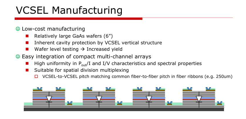
Figure 8. Arrays of VCSELs used for driving multiple channels. Source: E. Temporiti. “VCSEL-based Solutions: Components, Circuits and Integration” ISSCC 2026
VCSELs are very popular in short reach communications for a numbers of reasons:
Low cost manufacturability - they are easy to test on-wafer across multiple samples
Scalability - they can be formed in “arrays” to drive multiple optical lanes
However, VCSELs do have some drawbacks:
Reliability - issues due to oxide confinement and high currents degradating mean-time-to-failure
Signal switching nonidealities, including:
Turn on delay - a delay in the turn on of the signal that adds to latency
Jitter - uncertainty in the signal edge that degrades BER
Relaxation oscillation - an “underdamped” response in the turn-on characteristic that can affect BER and signal quality
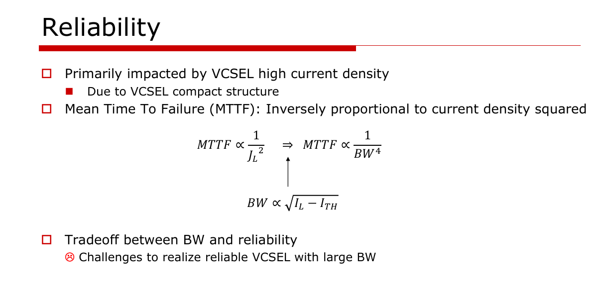
Figure 9. Tradeoff between Reliability and BW in VCSELs. Source: E. Temporiti. “VCSEL-based Solutions: Components, Circuits and Integration” ISSCC 2026
The main tradeoff in VCSELs is between BW and reliability. Higher current densities allow for higher BWs, but it also decreases the mean time to failure, a common metric used when evaluating reliability.
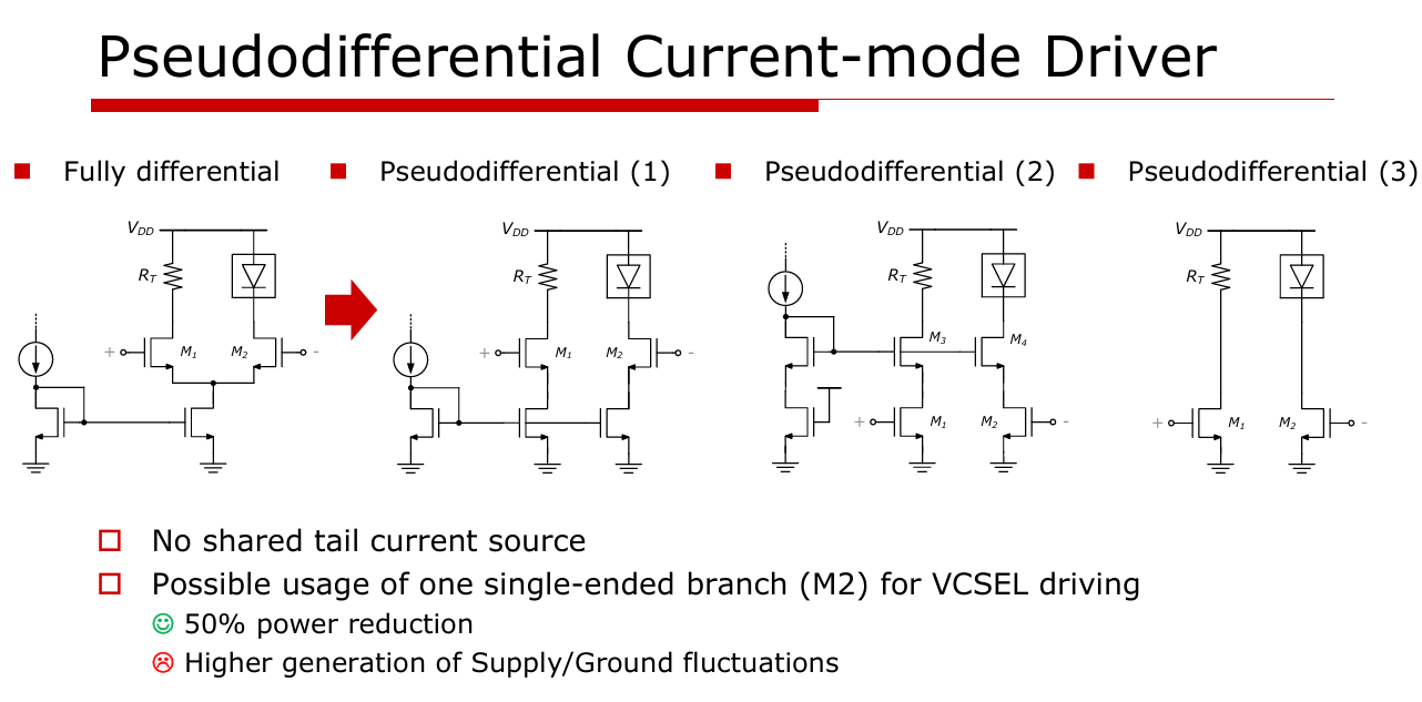
Figure 10. Pseudodifferential methods to drive the VCSEL directly. Source: E. Temporiti. “VCSEL-based Solutions: Components, Circuits and Integration” ISSCC 2026
Here are a few DC coupled, common anode circuits used to to drive the laser directly using either fully differential or pseudodifferential to convert a voltage to a current to drive the VCSEL. There are other methods of driving such as common-cathode, BJTs, and push-pull implementations depending on the requirements of the system.
In general, the more VCSEL current that is needed, the slower the driver will be due to increasing output capacitance.
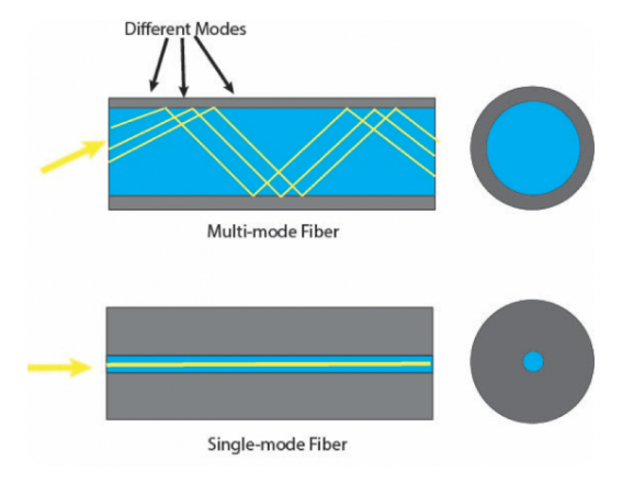
Figure 11. Single mode vs Multi-mode fibers. Source: https://blogs.cisco.com/sp/fiberopticspt2singlemultifiber
Multimode fiber optic cables are primarily constructed from silica glass (silicon dioxide). There are two major categories of fiber for high speed communications:
Multimode - Uses a larger core (50–62.5 um) to transmit multiple light paths
There are five classifications, OM1-5, that grade the quality of the fiber.
Pros: Cost-effective for short-distance, high-speed applications
Cons: Limited distance due to higher signal modal dispersion
Single Mode - Uses a smaller core (8-10um) to transmit a single mode of light
Pros: Low signal loss, avoids modal dispersion
Cons: Higher cost of laser components and more complex installation requirements
Generally speaking, multi-mode fibers are used for short reach interconnect due to its low cost and complexity. However, single mode fiber is being evaluated to “future proof” the data communications since it can support the higher BWs, though it adds to cost and integration complexity.
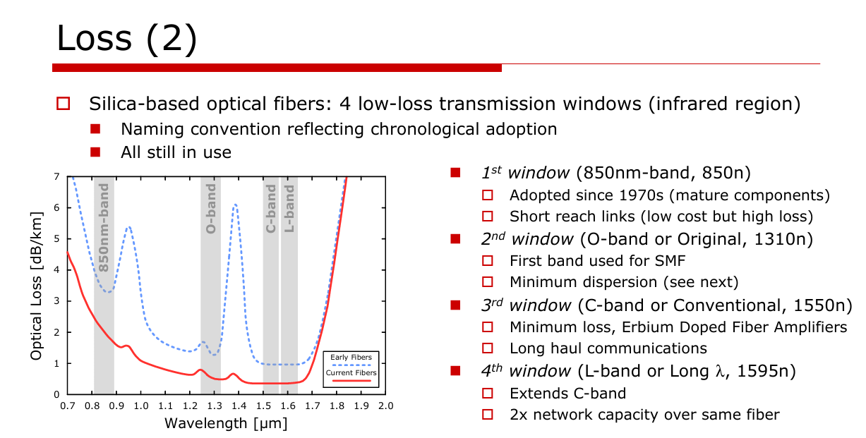
Figure 12. Transmission windows used in silica-based optical fibers. Source: E. Temporiti. “VCSEL-based Solutions: Components, Circuits and Integration” ISSCC 2026
There are also four wavelength bands used in the fiber:
850nm band - used for short reach links
O-Band - 1310nm
C-band - 1550nm
L-Band - Extends C band to allow 2x network capacity
There are four major impairments:
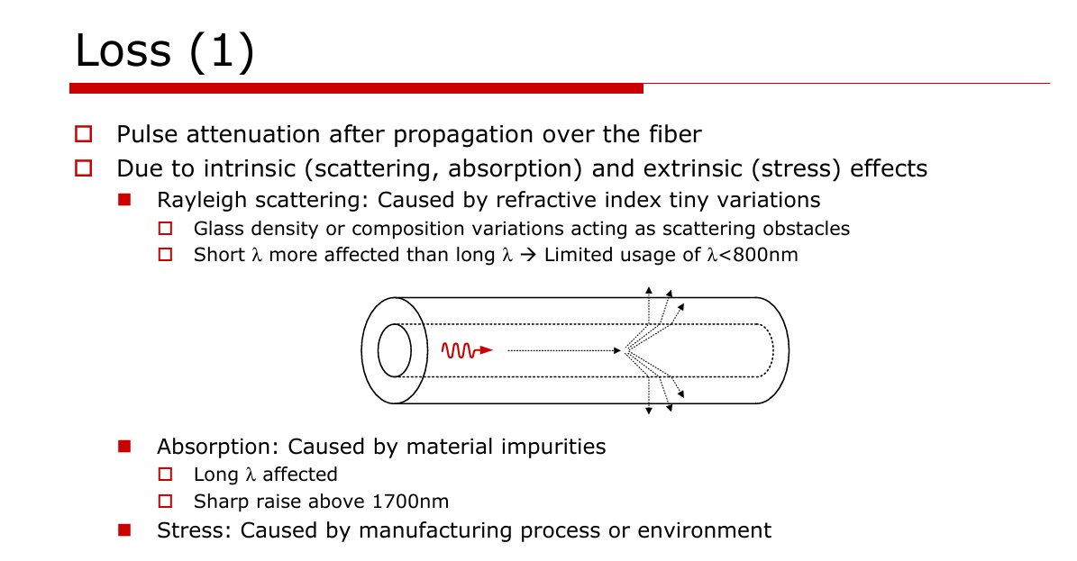
Figure 13. Losses in the Fiber. Source: E. Temporiti. “VCSEL-based Solutions: Components, Circuits and Integration” ISSCC 2026
Loss. Losses cause pulse attenuation after propagation from a fiber. These are caused by intrinsic sources, including
Rayleigh Scattering
Absorption
Manufacturing Stress
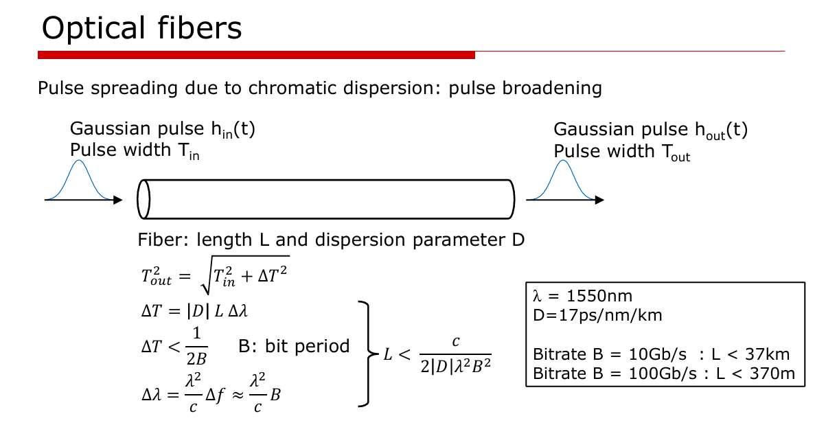
Figure 14. Chromatic Dispersion. Source: P. Ossieur. “Introduction to Optical Communication Systems From VCSELs, integrated photonics to coherent solutions” ISSCC 2026
- Chromatic Dispersion - pulse spreading after propagation over the fiber. This is caused by fiber refractive index dependence on wavelength
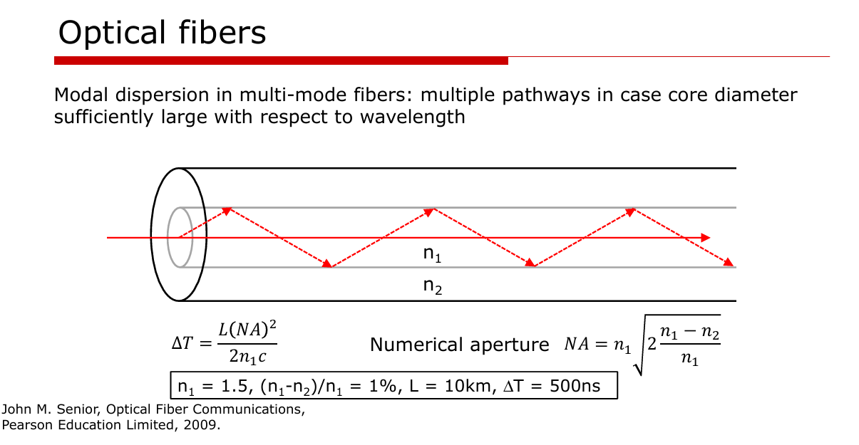
Figure 15. Modal Dispersion in Multi Model fibers. Source: P. Ossieur. “Introduction to Optical Communication Systems From VCSELs, integrated photonics to coherent solutions” ISSCC 2026
- Modal dispersion - distortion due to different propagation delays of different optical modes. Modal dispersion matters in multimode fiber.
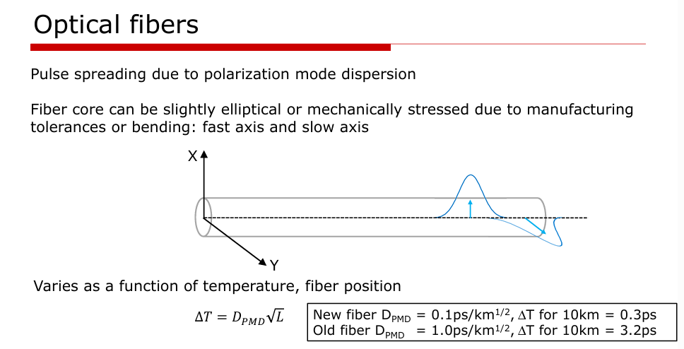
Figure 16. Polarization Mode dispersion in optical fibers. Source: P. Ossieur. “Introduction to Optical Communication Systems From VCSELs, integrated photonics to coherent solutions” ISSCC 2026
- Polarization Mode dispersion (PMD) - dispersion cause by pulse spreading of different polarizations due to asymmetries in the fiber core.
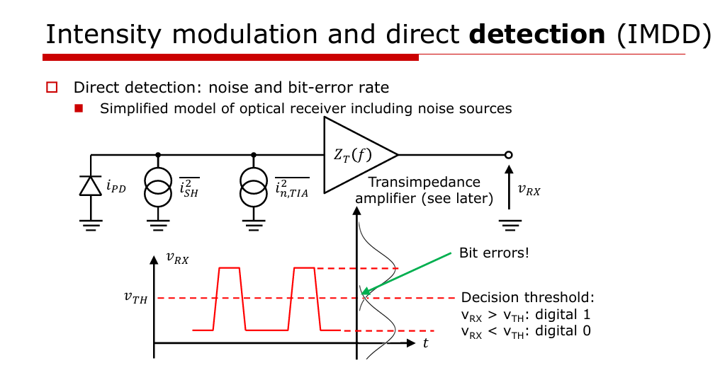
Figure 17. Direct detection of an optical signal. Source: P. Ossieur. “Introduction to Optical Communication Systems From VCSELs, integrated photonics to coherent solutions” ISSCC 2026
A photodetector consists of a Reverse biased PIN junction that generates current proportional to the detected light. The transimpedance amplifier then amplifies this current to an output voltage at the other end.
There are some important specs of this system:
PIN characteristics: Responsivity, capacitance, noise, dark current
Receiver Q-factor: The received signal level relative to total receiver noise
BER: BER can be derived from this Q factor: BER = 1/2*erfc(Q/sqrt(2))
A higher extinction ratio is desired to ease the burden on the receiver, but it does come with a higher power usage.
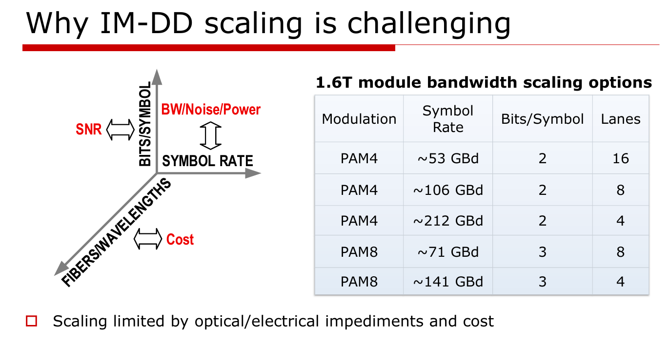
Figure 18. The three “axes” of scaling IM-DD and associated tradeoffs: Bits/symbol imposes an SNR penalty, symbol rates affects BW/Noise/Power, and Fibers/Wavelength affects cost/complexity. Source: P. Hanumolu. “Analog and Mixed-Signal Approaches for Low-Complexity Coherent Optical Links” ISSCC 2026
Scaling IM-DD to higher data throughputs is hard due to several unfavorable tradeoffs between BW, reach, noise, power, SNR, and cost. These include effects in both optical and electrical domain themselves:
Optical
Chromatic dispersion
Polarization Mode dispersion (PMD)
Nonlinear and interference effects
Electrical
Noise penalties at Higher BW
Tighter jitter, skew, and ISI
BW scaling limits in front ends
You can have the fastest optical transceiver, fiber, but its pointless if the signal can’t get to it fast enough. Not only the optical receiver itself needs to improve, but the signal integrity from the electrical interconnect is running into challenges shuttling high speed data back and forth. Solutions need to ensure that speed “bottlenecks” within the system scale with the system demands.
This leads to four major trends that generally increase complexity:
Co-packaged optics - embedding optical components within the package itself
Silicon Photonics - routing light through silicon waveguides and modulating it
External modulation - modulating a continuously running laser for higher BW
Coherent Optics - modulation amplitude and phase in the optical domain
After the paywall I’ll discuss these in further detail.
第二部分:解析(深度解读)
文章核心论点摘要
- 短距光互连的主力是 IM-DD(强度调制-直接检测):用光强(0/1 或 PAM4 多电平)编码、直接检测恢复,封装成可插拔光模块。AI 数据中心对 224+ Gbps 的需求,逼迫光模块本身与”宿主芯片 → 光引擎”的电互连信号完整性同步升级。
- 先把组件拆到底,再看缩放瓶颈:文章把 IM-DD 拆成发射端(激光器/VCSEL + 驱动)、光纤、接收端(PIN + TIA)三块,逐一对激光器原理、VCSEL 权衡、光纤模色散、接收端 Q 因子/BER 做了第一性原理讲解。
- IM-DD 缩放受”三轴”约束:Bits/symbol(越高 SNR 惩罚越大)、Symbol rate(影响带宽/噪声/功耗)、Fiber/Wavelength(影响成本/复杂度)。光域与电域的损伤会同时恶化。
- 四大趋势提升复杂度(付费深解):共封装光学(CPO)、硅光(SiPh)、外调制、相干光学——公开免费部分只给了一句话定位,详细展开在付费墙后。
关键概念解读
- IM-DD(Intensity Modulation Direct Detection):强度调制-直接检测。用光强编码信息,接收端用光电二极管直接检波。短距光通信的绝对主力,成本低、结构简单。
- PAM4:4 电平脉冲幅度调制。单个波长一次传 2 bit,翻倍符号效率,但电平间距变小、对 SNR 余量要求更紧。
- VCSEL(垂直腔面发射激光器):圆形截面、垂直出光,多量子阱增益 + 上下 DBR(分布布拉格反射镜)。850 nm GaAs 用于多模短距;1310/1550 nm InP 用于单模长距。
- DFB 激光器(分布式反馈):靠周期光栅(布拉格反射镜)选频,线宽窄、波长稳定,是高速外调制光源(EML)与外置光源(CW laser)的基础。
- 直接调制 vs 外调制:直接调制=电信号直接拉高/拉低激光功率;外调制=用一个稳频连续激光器,外加调制器(MZM 等)加载信号,带宽更高、啁啾更小,是 800G/1.6T 以上主流。
- 消光比(Extinction Ratio):P1/P0。越高接收端 BER 余量越好,但需要更大驱动电流 → 更高功耗。
- 多模 vs 单模光纤:多模(芯径 50–62.5 µm)成本低、短距友好,但受模间色散限制距离;单模(8–10 µm)低损耗、无模间色散,但激光与部署成本更高,被视为”面向未来”的升级路径。
- 四大光纤损伤:损耗(瑞利散射/吸收/应力)、色度色散(折射率随波长变化)、模间色散(多模特有)、偏振模色散 PMD(纤芯不对称)。
- 接收端 PIN + TIA:反偏 PIN 产生与光强成正比的光电流,跨阻放大器(TIA)转成电压。Q 因子衡量”信号相对总噪声”,BER = ½·erfc(Q/√2)。
- 信号完整性瓶颈:最快的光模块若”宿主 die → 光引擎”的电互连跟不上也白搭——高速电互连的抖动、偏移(skew)、码间干扰(ISI)正成为系统级瓶颈。
组件分层拆解
| 组件 | 核心内容 | 技术要点 / 权衡 |
|---|---|---|
| 发射端:激光器 / VCSEL | IM-DD 光源;VCSEL 可阵列化驱动多通道 | 低成本、可晶圆级测试、可阵列;但存在可靠性 vs 带宽权衡(电流密度↑→带宽↑,但平均失效时间↓);开关非理想性:开启延迟、抖动、弛豫振荡 |
| 发射端:驱动电路 | 全差分 / 伪差分把电压转电流驱动 VCSEL | 所需电流越大,输出电容越大、驱动越慢;还有共阴极、BJT、推挽等拓扑 |
| 光纤 | 多模 vs 单模;四个波长窗口(850nm / O 1310 / C 1550 / L 扩展) | 短距多用多模省成本;单模”未来验证”但贵且复杂 |
| 接收端 | 反偏 PIN + TIA | 关注响应度、电容、噪声、暗电流;Q 因子 → BER;高消光比减轻接收负担但增功耗 |
IM-DD 缩放”三轴”与损伤
| 缩放轴 | 含义 | 带来的代价 |
|---|---|---|
| Bits / symbol | 提高每符号比特(如 PAM4) | SNR 惩罚变大 |
| Symbol rate | 提高符号率 | 带宽↑、噪声↑、功耗↑ |
| Fiber / Wavelength | 换光纤 / 加波长 | 成本↑、集成复杂度↑ |
光域损伤(色度色散、PMD、非线性/串扰)与电域损伤(高带宽噪声惩罚、更紧的抖动/偏移/ISI、前端带宽极限)会叠加恶化,这正是高速率下系统级瓶颈的来源。
四大技术趋势(付费段仅列名,原文未展开)
| 趋势 | 一句话定位 |
|---|---|
| Co-packaged Optics (CPO) | 把光组件嵌入封装内部,缩短电互连 |
| Silicon Photonics (SiPh) | 用硅波导导光并调制,走 CMOS 工艺规模经济 |
| External Modulation | 调制连续运行激光器以获得更高带宽 |
| Coherent Optics | 在光域同时调制幅度与相位,提升频谱效率与长距能力 |
⚠️ 以上四项的详细技术展开在原文付费段(”After the paywall I’ll discuss these in further detail”)。本文仅含公开免费部分,不构成对四大趋势的完整技术结论。
与本站投资视角的连接
这篇文章是理解本站另外三篇光投资文章的技术地基:
- 《Why You Should Be Watching Optical Test》(光测试五大瓶颈):正对应本文”线速率越高 → 抖动/ISI/噪声越紧、测试越难”的结论——测试瓶颈不是凭空来的,根源在 IM-DD 缩放三轴与电域损伤。
- 《The 100-Second Bottleneck Behind NVIDIA CPO》(CPO 测试栈):本文点出的”信号完整性瓶颈”“外调制/CPO 趋势”解释了为什么 CPO 量产瓶颈从制造转向测试。
- 《Damnang’s Optical Investment Map v1.0》(7 层价值链):本文的 VCSEL/DFB/EML(L2 有源器件)、TIA/驱动器/DSP(L3 连接 IC)、PIN/TIA 与测试(L7),正是那条价值链底部技术栈的”是什么”。
简言之:谁掌握了激光器(EML/CW laser)、调制器、TIA/驱动器与晶圆级测试,谁就卡住了 AI 光互连的价值链咽喉——这与三篇投资文的逻辑一脉相承。
风险提示
- 本文为技术科普,非投资建议:内容聚焦原理与架构,不构成任何买卖建议。
- 付费边界:四大趋势的详细展开、原文可能的性能数据与路线判断在付费段,本文未含。
- 技术时效性:文中图表多引自 ISSCC 2026 公开演讲,具体参数与厂商路线会快速演进,请以最新原文/厂商资料为准。
- 技术路径风险:CPO / 硅光 / 相干光学的渗透节奏与最终胜出架构尚未定局,相关标的受技术路线切换影响大。
本文仅供学习交流,不构成投资建议。原文版权归原作者所有。