The Critical Bottleneck in CPO Mass Production? It's Testing — CPO 测试的市场机会
TrendForce 深度解析 CPO 量产的真正瓶颈不在封装而在测试,拆解四大测试阶段与 Advantest、Teradyne、Keysight、Chroma、Enlitech 等设备的竞争格局;本文含英文原文 + 中文深度解读。
本文整理自 TrendForce(insights.trendforce.com),原文发布于 Apr 24, 2026(标题原文:The Critical Bottleneck in CPO Mass Production? It’s Testing)。 结构为 正文(英文原文)+ 解析(中文深度解读),方便中英对照阅读。 来源说明:内容经公开页面获取;本发布保留完整英文原文并附中文深度解读,仅作信息整理与学习用途,著作权归原作者所有,建议在原站支持作者订阅。
第一部分:正文(Original Article)
The Critical Bottleneck in CPO Mass Production? It’s Testing
TrendForce 2026 New York Roadshow arrives May 12. We’re decoding the AI-driven market inflections in memory and foundry — and what they mean for the 2026–2028 supercycle: REGISTER HERE.
As AI data center clusters continue to scale, the demand for data movement has surged, pushing traditional copper interconnects to their physical limits. CPO is now widely regarded as one of the key interconnect solutions for next-generation AI infrastructure. With TSMC’s COUPE platform projected to enter volume production in 2026, CPO is making its transition from the lab toward commercialization.
However, the CPO inspection and testing phase remains a significant hurdle. Currently, the industry lacks unified standards, and processes remain largely manual, making testing one of the major bottlenecks holding back CPO chip mass production.
This article examines the technical challenges of CPO testing, provides a detailed breakdown of the four critical testing stages, and maps out the existing solutions and technical advantages of equipment vendors.
Related report: AI Interconnect Outlook: NVIDIA Leads the Transition to CPO and Silicon Photonics Architectures
What Makes CPO Testing So Challenging
Co-Packaged Optics (CPO) integrates optical components into a Photonic Integrated Circuit (PIC), which is then co-packaged with an Electrical Integrated Circuit (EIC) in a single chip. By replacing electrical traces with optical paths, CPO reduces power consumption and latency. The bonded PIC-EIC assembly is called an Optical Engine (OE).
TSMC’s COUPE (Compact Universal Photonic Engine) is one such implementation, using SoIC Face-to-Face (F2F) stacking to hybrid-bond the EIC directly onto the PIC, incorporating shallow dielectric vias (TDV), embedded microlenses, and metal reflectors.
Unlike traditional EIC testing, which is purely electrical, a PIC contains a large number of optical components such as couplers, modulators, photodetectors (PD), optical filters, and optical waveguides. Testing an OE requires expertise across electrical, optical, and optoelectronic interactions, significantly increasing test complexity.
PIC testing must measure parameters such as insertion loss (IL), polarization-dependent loss (PDL), responsivity, waveguide propagation loss, and optical crosstalk. However, there is currently no unified test standard for these.
In addition, precise alignment of optical probes is a major challenge. The technique of guiding external light from an optical fiber into the OE’s optical waveguide is called optical coupling. However, a single-mode fiber core has a cross‑sectional area of about 78.5µm², while that of an optical waveguide is only about 0.099µm², a difference of nearly 800 times. Without nanometer-level alignment precision, coupling loss will be enormous.
Therefore, the fiber array of the optical probe must maintain a precise gap from the wafer or die surface while finely adjusting its angle relative to the coupler to maximize optical power transfer, and then perform measurements sequentially across different wavelength ranges. Such delicate operations currently rely on manual handling, with 100% inspection of a single PIC taking on average more than 100 seconds, making this one of the key bottlenecks for mass production of CPO chips.
The Four Testing Stages, and Why OWAT Matters Most
The testing stages required for a single CPO chip are:
(1) PIC wafer‑level test: DC electrical and optical tests, such as basic optical measurements of power, loss, dark current, etc.
(2) EIC‑PIC wafer‑level test: modulation‑function tests (electro‑optic, opto‑electric, and opto‑optic), high‑speed tests, and S‑parameter measurements.
(3) OE‑level test: full‑flow calibration, DC tests, high‑speed tests, optical loop‑back tests, and S‑parameter measurements. This is the key stage for confirming “Known Good Optical Engines” (KGOE).
(4) Advanced‑package module‑level test: full system functional verification and optical loop‑back tests.
Among these, PIC wafer-level test, also known as OWAT, is the most critical stage. While PICs are typically fabricated on mature process nodes, EICs generally use advanced nodes. If defective PICs can be identified already at the wafer stage, before bonding with expensive EICs, then scrapping of EICs and subsequent process losses can be greatly reduced.
Competitive Structure of Supply Chain
Traditional EIC automated test equipment (ATE) market is dominated by Japan’s Advantest and the US’s Teradyne. Since developing CPO test equipment requires expertise in both EIC and PIC testing, both vendors have pursued partnerships with PIC probe specialists: Advantest with FormFactor, and Teradyne through its 2025 acquisition of Quantifi Photonics and collaboration with ficonTEC.
Advantest & FormFactor
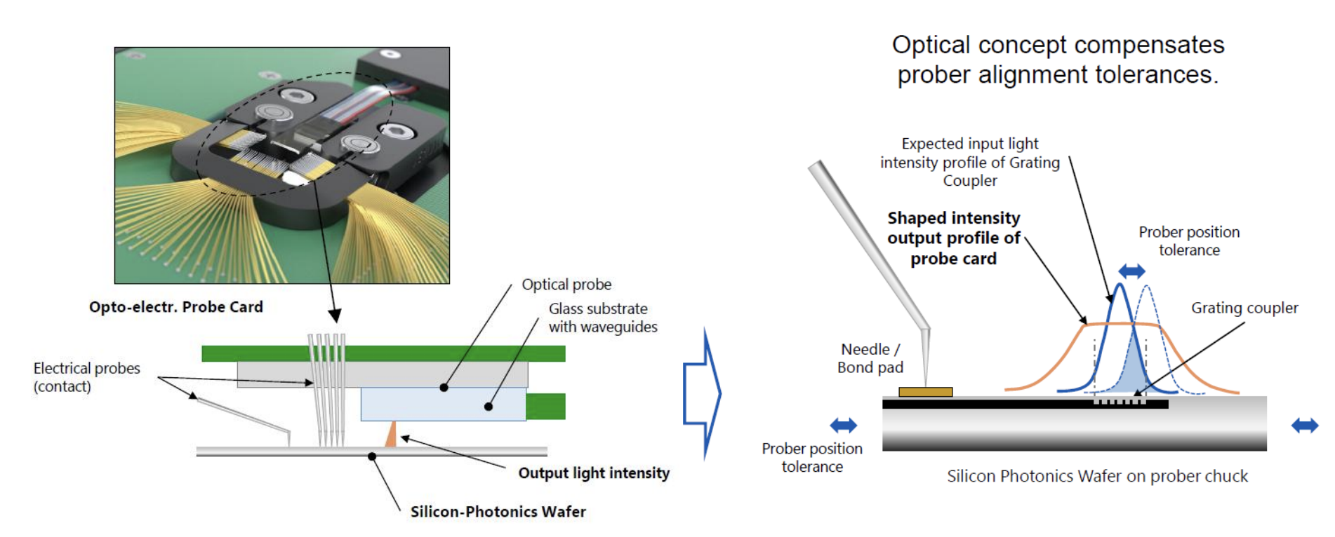
In June 2024, Advantest, Jenoptik, and Ayar Labs jointly launched the UFO Probe Card, integrating both electrical and optical probes on a single card for simultaneous electro-optical testing. Its key innovation is alignment tolerance compensation technology: the optical probe’s output beam is specifically shaped, allowing the optical signal to enter the PIC coupler even with slight prober positioning errors, greatly reducing alignment time.
 Source: Advantest
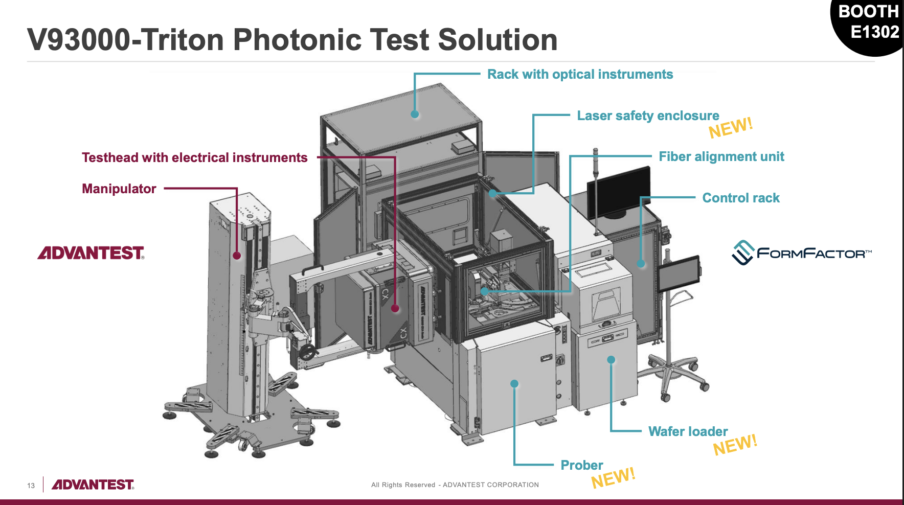
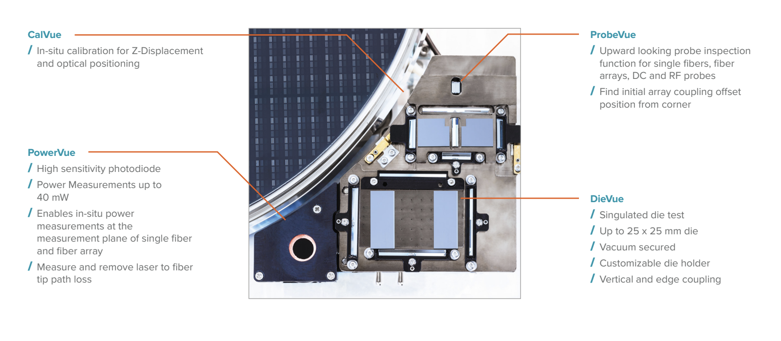
In April 2025, Advantest and FormFactor launched the V93000-Triton photonic test system, featuring 9-axis photonic alignment and FormFactor’s OptoVue Pro optical alignment system. Its CalVue technology enables in-situ calibration of Z-axis displacement and optical positioning by observing the fiber array via uniquely designed retro-mirror technology and applying automated machine-vision algorithms in real time, reducing fiber alignment time.
 Source: Advantest
 Source: FormFactor
Teradyne & ficonTEC
In March 2025, Teradyne and Germany’s ficonTEC (now a subsidiary of China’s Robo Technik) announced the industry’s first high-volume 300 mm double‑sided wafer probe test system for silicon photonics. ficonTEC provides the WLT‑D2 double‑sided wafer test platform, which features 50 nm‑range precision alignment, while Teradyne supplies the UltraFLEXplus ATE and IG‑XL system software.
A key feature of ficonTEC’s WLT‑D2 is its dual‑sided test capability, enabling simultaneous electrical testing on the top surface and optical testing on the bottom surface of the wafer, thereby improving test efficiency. The subsequent DLT‑D1 is a dual‑sided die‑level test system that can connect up to three parallel test heads simultaneously, increasing throughput and reducing test cost. With the addition of the DLT‑D1, ficonTEC now offers a complete CPO test product portfolio from wafer‑level to die‑level.
Chroma
Chroma is the global leader in SLT equipment. Its photodiode burn‑in and reliability test systems, the Model 58604/58604‑C/58606 series, are designed for reliability testing of PIC components such as 3D sensing devices, LDs, PDs, and modulators. The Model 58606 provides 256 SMU channels per module layer, and can be configured with up to 7 layers, for a total of 1,792 channels. Leveraging its optical test expertise at the SLT stage, Chroma has also announced that it is investing in the development of CPO test equipment.
Keysight
Keysight, the global leader in measurement instruments, is well known for its high‑speed test equipment and also provides a complete PIC wafer‑test solution. Keysight’s PIC wafer‑test solution is integrated with FormFactor, and is compatible with FormFactor’s Velox prober control software.
Keysight’s N778x series polarization synthesizers can rapidly switch the incident light among different States of Polarization (SOP), and, together with the N7700100C Polarization Lambda Scan (LS) software, uses matrix methods to derive IL, PDL, TE/TM IL, and other parameters. Therefore, this solution does not need polarization‑maintaining fiber (PMF), nor does it require prior manual polarization correction at multiple wavelength points, greatly increasing test efficiency. In addition, its SOP stabilization technology can lock the input light’s polarization state at a specific point, ensuring stable optical coupling throughout the entire wavelength sweep.
Enlitech
In September 2025, Enlitech partnered with iST to launch Night Jar, a SiPh chip testing platform. Designed as an add-on hyperspectral imaging analysis system, it can be directly mounted onto probe stations of any brand across various testing stages (WAT, CP, FT, etc.). This platform addresses long-standing industry pain points: previously, light leakage locations in optical waveguides could only be roughly estimated using reflected light, yielding only total or average optical loss values.
The Night Jar platform is distinguished by its ability to precisely pinpoint light leakage and measure quantitative IL values for specific waveguide segments or optical components. By visually mapping these metrics and supporting wafer-level optical loss mapping, the platform enables R&D personnel to identify defects more accurately and rapidly, ultimately improving production yields.
Market Opportunities
As chip designs grow increasingly complex, the difficulty of SoC testing has risen significantly. The number of test stations and the overall testing time required for a single chip continue to increase, driving up the share of test equipment within total semiconductor equipment capital expenditures. As CPO chips are integrated into product portfolios, the semiconductor sector’s capital expenditures on test equipment are expected to climb even further.
The CPO test equipment market is taking shape, and knowing the competitive landscape matters. For the comprehensive supply chain and market analysis, access the full report:
CPO Testing Revolution: Market Opportunities in Co-Packaged Optics Validation
第二部分:解析(深度解读)
一、这篇文章为什么重要
市场普遍认为 CPO(共封装光学)的产业化瓶颈在”能不能把光引擎做出来、封装好”,但这篇文章把视角拉到了被严重低估的环节:测试(Testing)。TrendForce 的核心判断是——CPO 从实验室走向量产,真正的卡点是”检测与测试”,而不是芯片设计或封装本身。
为什么这个判断关键?因为 CPO 的产业链价值分布会被重新定义。当 TSMC 的 COUPE 平台在 2026 年进入量产,意味着上游制造(foundry、封测)开始成熟,但下游”能不能以可接受的成本和良率把合格光引擎筛出来”会成为新的稀缺能力。谁能解决测试瓶颈,谁就能在 CPO 放量周期里吃到设备资本开支(Capex)的增量蛋糕。
这与 2025—2028 的 AI 基础设施超级周期直接相关:AI 集群对数据搬运(data movement)的渴求把铜互连推到物理极限,CPO 是公认的下一代入口方案之一。当大家都在盯光模块、硅光芯片、光源(laser)时,测试设备是一条”卖铲子”的确定性赛道——无论最终哪家 CPO 方案胜出,都要买测试机台。
二、核心论点拆解
文章主线可以拆成三个层次:为什么难 → 测什么、在哪测 → 谁在布局。
| 维度 | 核心论点 | 关键数据/事实 |
|---|---|---|
| 难在哪 | PIC 含大量光学元件,测试横跨电学、光学、光电交互,无统一标准 | 测试参数涵盖 IL / PDL / 响应度 / 波导传输损耗 / 光串扰 |
| 耦合之难 | 单模光纤纤芯截面 ~78.5µm² vs 波导 ~0.099µm²,相差近 800 倍 | 需纳米级对准精度,否则耦合损耗巨大 |
| 效率之痛 | 单颗 PIC 100% 检测平均 >100 秒,且高度依赖人工 | 这是 CPO 量产的核心瓶颈之一 |
| 四大阶段 | PIC 晶圆级测试(OWAT)、EIC-PIC 晶圆级、OE 级、先进封装模组级 | OWAT 最关键:在键合昂贵 EIC 前筛掉坏 PIC |
| 格局 | 传统 ATE 由 Advantest、Teradyne 双寡头主导,需联手 PIC 探针专家 | Advantest+FormFactor;Teradyne 收购 Quantifi Photonics(2025)+ficonTEC |
| 增量玩家 | Chroma(SLT 龙头)、Keysight(仪表龙头)、Enlitech+iST(缺陷成像) | 各凭原有优势切入 CPO 测试 |
文章的”胜负手”判断在于:OWAT(PIC 晶圆级测试)是四个阶段中最关键的一环。逻辑很硬——PIC 多用成熟制程、EIC 多用先进制程,如果在晶圆阶段就筛掉缺陷 PIC,就能避免把昂贵的 EIC 白白报废。这是典型的”测试前移(shift-left)”降本逻辑,也是设备商差异化竞争的主战场。
三、关键概念 / 技术解读
1. Optical Engine(OE)与 COUPE 结构。 CPO 把 PIC(光子集成电路)和 EIC(电集成电路)键合在一起叫 OE。TSMC 的 COUPE 用 SoIC Face-to-Face(F2F)混合键合,把 EIC 直接叠到 PIC 上,并集成浅介孔(TDV)、嵌入式微透镜、金属反射镜——这些是光从 EIC 侧向波导高效耦合的关键微结构,也是测试要对准的物理目标。
2. 光学耦合(Optical Coupling)与对准精度。 这是全篇最硬的工程约束:单模光纤纤芯截面约 78.5µm²,波导仅约 0.099µm²,相差近 800 倍。形象地说,相当于要把一束光精准地灌进一根比自己细近 30 倍(线性尺寸)的”针管”里,误差在纳米级。这就是为什么光纤阵列探针必须保持精确间隙、微调角度,并在不同波长区间顺序测量——也解释了为什么单颗检测要 100 秒以上。
3. 四大测试阶段各自的职责。
- (1) PIC 晶圆级(OWAT):DC 电学 + 基础光学(功率/损耗/暗电流)。
- (2) EIC-PIC 晶圆级:调制功能(电-光、光-电、光-光)、高速、S 参数。
- (3) OE 级:全流程校准、DC、高速、光环回(loop-back)、S 参数——确认”Known Good Optical Engines(KGOE)”的关键站。
- (4) 先进封装模组级:全系统功能验证 + 光环回。
4. 偏振相关损耗(PDL)与偏振合成器。 光芯片测试要测 IL(插入损耗)、PDL(随偏振态变化的损耗)、TE/TM 模式 IL。Keysight 的 N778x 偏振合成器在不同偏振态(SOP)间快速切换,配合 N7700100C 偏振波长扫描软件用矩阵法直接解算这些参数——好处是不需要保偏光纤(PMF),也不需要人工逐波长点校准偏振,效率大幅提升。其 SOP 稳定技术还能在整个波长扫描中锁住输入光的偏振态,保证耦合稳定。
5. 双面对准与”双面测试”。 ficonTEC 的 WLT-D2 做到 50nm 级精度、300mm 双面晶圆探针:上面测电、下面测光,同期进行。DLT-D1 进一步做到晶粒级双面对测,最多并联 3 个测试头提吞吐。这是”并行化”降本的另一条技术路径。
6. 缺陷可视化(Enlitech/iST Night Jar)。 传统上波导漏光位置只能靠反射光粗略估计,只能得到总损耗或平均损耗;Night Jar 用附加的高光谱成像直接挂到任意品牌探针台上,能精确定位漏光点、给出具体波导段/元件的量化 IL,并支持晶圆级光损耗分布图——直击良率提升的痛点。
四、与本站其他 CPO / 硅光系列文章的链接
- CPO 最大瓶颈:高良率测试(cpo-biggest-bottleneck-high-volume-testing):与本文主题高度互补,本文从设备商格局切入,该文聚焦量产良率测试难题。
- CPO 幻象?CPO 专题终章(the-illusion-of-cpo-cpo-special-final):理解 CPO 商业化预期与现实的落差。
- 光学入门(三):共封装光学(optics-primer-part-3-co-packaged):补充 CPO 结构与封装基础。
- TSMC 领先 CPO、三星第三芯片(tsmc-ahead-in-cpo-samsung-third-chip):对照 COUPE 平台量产节奏,理解本文”2026 量产”判断的制造侧背景。
- 硅光链路预算与光学非理想性(silicon-photonics-link-budget-and-optical-nonidealities):深入 IL / 损耗预算,与本文测试参数呼应。
五、投资意义
文章指向一条”卖铲子”的确定性赛道——CPO 测试设备。无论最终 CPO 采用哪家方案(NVIDIA、Broadcom、TSMC COUPE 等),量产都绕不开测试机台,因此测试设备商的订单弹性与 CPO 放量强相关。
- Advantest(TYO: 6857):与 FormFactor、Jenoptik、Ayar Labs 合作的 UFO Probe Card + V93000-Triton(9 轴对准、OptoVue Pro、CalVue 在线校准),是直接受益的 ATE 龙头。
- Teradyne(NASDAQ: TER):通过 2025 年收购 Quantifi Photonics + 联手 ficonTEC(WLT-D2/DLT-D1 双面测试),补齐硅光测试能力,与 Advantest 形成双寡头竞争。
- FormFactor(NASDAQ: FORM):探针卡与 OptoVue Pro 光学对准系统,是 Advantest/Keysight 方案的关键拼图,双面/光学对准的卡位价值突出。
- Keysight(NYSE: KEYS):仪表与 PIC 晶圆测试方案龙头,N778x 偏振合成器 + SOP 稳定技术构成差异化壁垒。
- Chroma(TW: 2360):SLT 龙头,58606 高达 1792 通道 SMU,凭 SLT 阶段光测经验切入 CPO 测试,是台股潜在受益标的。
- Enlitech / iST(TW: 3289):Night Jar 缺陷成像平台,提供晶圆级光损耗分布,良率提升工具属性强。
- ficonTEC:已被中国 Robo Technik 收购,其双面测试平台是 Teradyne 方案的核心;关注国产设备供应链替代机会。
对 A 股/台股/日股投资人而言,测试设备的”前移(OWAT)”与”双面并行”是两条最值得跟踪的技术路线,对应设备商的订单兑现节奏与 ASP(平均售价)提升空间。
六、风险提示
- 量产节奏风险:本文假设 TSMC COUPE 2026 年量产,若 CPO 规模化延期,测试设备 Capex 增量将后移,相关设备商业绩兑现慢于预期。
- 标准缺失风险:文章明确指出行业尚无统一测试标准,标准走向可能让部分早期方案被淘汰或需二次投入。
- 人工依赖与降本不及预期:单颗 PIC >100 秒、高度人工的现状若自动化突破慢,将拖累 CPO 整体良率与成本曲线。
- 竞争格局变化:双寡头(Advantest/Teradyne)之外,Chroma、Keysight、Enlitech 及中国设备商(如 ficonTEC 中资背景)可能改变份额分布,估值已部分反映预期。
- 下游集中度:CPO 测试需求高度依赖少数 hyperscaler / 芯片厂(NVIDIA、Broadcom 等)的导入决策,客户集中带来订单波动风险。
以上解读基于原文信息整理,不构成投资建议。