通往 CPO 之路上的 NPO:高带宽需求下的高能效互连 — NewPhotonics NPC50503 解读
NewPhotonics 的立场文:电墙在 200Gbps/lane 已逼近极限,NPO 用可插拔、可维护的近封装光引擎做过渡;NPC50503 1.6T 以光域信号处理替代 DSP,主张功耗降 20%、补偿 12dB RF 损耗。文中逐条标注厂商主张与待验证边界。
来源:NewPhotonics — On The Road to CPO: NPO for High-Demand Bandwidth in Energy-Efficient Interconnect 原文链接:https://newphotonics.com/on-the-road-to-cpo-npo-for-high-demand-bandwidth-in-energy-efficient-interconnect/ 原文发布日:2026-01-13(2026-01-14 更新)| 作者:Amelia(NewPhotonics) 本页内容:Part 1 英文原文全文 + Part 2 中文深度解读 ⚠️ 立场提示:本文是 NewPhotonics 官方博客,主旨是推介自家的 NPC50503 1.6T NPO 发射器。文中所有性能数字均为厂商自述,未经独立第三方验证。解读部分(Part 2)会逐条标出哪些是可直接采信的产品定义、哪些是需要外部复现的营销主张。
第一部分:正文(Original Article / 英文原文)
On The Road to CPO: NPO for High-Demand Bandwidth in Energy-Efficient Interconnect
The race to evolve beyond the electrical limitations of Moore’s Law is on. All attention has turned to bringing complex new CPO systems to market that will maximize data consumption in more power-efficient data center infrastructure.
In the future, co-packaged optics will be the linchpin for AI factory expansion, from predominantly electrical to full-scale electro-optics. But AI isn’t waiting. Data centers need bandwidth and power efficiency to serve up the historic volume of artificial intelligence generated and demanded today, and it has to be scalable.
We’re taking a progressive approach to a serviceable laser-based solution: our product roadmap charts innovative technologies that address the complexity and market pressures characterized by demand-side speed and bandwidth expansion, alongside design-side requirements for a more energy efficient laser package. And we’re doing it without compromising reliability. The photonics-based data center is no longer a distant projection; we have designed silicon photonics chips to address the physical requirement for the AI factory right now.
At NewPhotonics, hyperscalers are discovering a pragmatic and partner-driven approach to high-bandwidth density at market-disrupting speed and power performance. While co-packaged optics continues along a path to maturity, we’ve introduced a near-packaged optics answer for the expanding data center need to meet AI driven demand. The NPC50503 1.6T NPO transmitter is designed to bridge the optical domain interconnect path from pluggable to CPO solutions in a more developed co-package ecosystem.
图1|NewPhotonics NPO 产品线题图(NewPhotonics 官方图片)
The Electrical Wall: Why We Must Move Closer to the ASIC
The standard, decades-old approach to data center networking can no longer rely solely on “front-panel” optics. In this model where digital electrical signals originate at the source (be it a GPU, Switch, or HPC processor), the high-speed data and performance expectations prevent it from efficient travel across the PCB to the front panel and through that standard OSFP module to converts the signal to optical – even for short versus long-haul transport.
The efficiency paradigm is starting to break now as speeds reach 200Gbps per lane and will cease to function entirely as we enter and go beyond the 400Gbps era. The physical distance the electrical signal must travel still matters, and as frequency increases, the “reach” of copper traces on a PCB continues to shrink. Maintaining signal integrity with greater data volumes at higher speeds even over a few inches is less and less effective – and certainly less energy efficient.
Rather than innovating to reduce power, contemporary architectures such as the addition of digital re-timers along the electrical path or replacing the PCB with direct copper cables simply preserve the existing state by utilizing high energy components and BOM cost that are not scalable.
While the CPO movement seeks to drive the E/O (electrical-to-optical) conversion point as close as possible to the ASIC to eliminate traces, moving directly from electrical to CPO introduces a new set of risks.
The NPO Advantage: Shortening the Stride to CPO
Near-packaged optics (NPO) represents a tactical evolution. By placing a pluggable optical engine with a socketed, near-packaged configuration, we achieve the signal integrity benefits of proximity without the reliability nightmares of full integration.
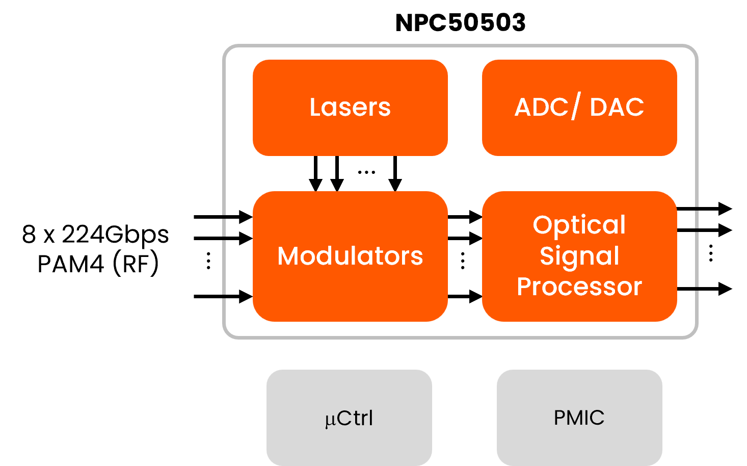
图2|NPC50503 框图:集成的 OSPic™ 全光信号处理器是方案差异化核心(NewPhotonics 官方图片)
The pluggable market offered significant advantages in compatibility and serviceability that CPO is struggling to meet. Consider a misbehaving optical link: with a hot-pluggable OSFP, a technician can simply swap the module. Current CPO designs, however, are far more complex. It may take a field technician a full day to shut down a rack, access the tray, and disassemble the entire system to reach an integrated optical module—some of which are soldered directly to the board.
The NPC50503 changes this calculation. It fits a serviceable plug that sits close enough to the source to maintain electrical integrity while retaining the modular characteristics of an OSFP. And it provides 1.6T interoperability at performance beyond today’s LPO-MSA compliance standards. This allows hyperscalers to immediately improve power efficiency while gaining crucial operational experience with integrated optics.
Breaking Capacity and Energy Constraints
Every innovation cycle since the Industrial Revolution has driven a “bubble-like” conundrum. The early telecom bubble was driven by infrastructure overbuild; the handheld compute bubble was driven by cloud demand. Today, we are experiencing a shift from CPU to GPU hardware that has created massive demand with limited gains in energy efficiency.
We are now entering a decade where the shift from electrical to Optical is mandatory. The transition from a 90/10 electrical/optical architecture to an optical-dominated scale is evolving faster than the power capability of our physical infrastructure. Real estate and rack space are finite, and the energy required to turn on more capacity often exceeds the power limitations of the local grid.
Industry leaders like NVIDIA are proclaiming new performance targets for hardware at 5x power reductions and 10x higher resiliency. However, these leaps often focus on the “Giant Data Center” of the future. They don’t account for optimizing the infrastructure where AI is running now.
With an NPO solution, advanced optical signal processing can affect power reductions of 20%, freeing that power to increase compute accessibility in the 500GW data centers currently nearing completion.
Introducing The NPC50503 laser integrated transmitter with integrated OSPic™ all-optical signal processor
The heart of our innovation is the NPC50503 1.6T NPO laser integrated transmitter chiplet featuring our OSPic™ all-optical signal processor. Unlike traditional solutions that rely solely on DSPs to correct signal impairments, our engine performs these functions in the optical domain. This direct connection to the SerDes is crucial to avoid DSP power consumption.
Laser integration carries many advantages like simpler assembly process, lower part count and higher yield, but prior attempts to integrate lasers directly inside a switch package were perceived as a substantial reliability risk. A single laser failure would necessitate replacing an entire, expensive switch ASIC.
Our approach offers a progression toward CPO with our laser-integrated solution. We utilize a reliable, low-loss coupling modality that is swappable with simple access to the ASIC fiber interface. This eliminates the need for an External Laser Source (ELSFP), which is often bulky, expensive, and complex to manage.
Our integrated laser provides higher reliability, with known-good-die and eliminates the need for system-wide re-architecture.
The Serviceability Dilemma: Minimizing Light Failure Risk
For hyperscale data center architects, the lack of modularity in early CPO designs was a “non-starter.” The NPC Series introduces the first-tier opportunity to deploy serviceable optical modules in the switch without significant cost or uptime losses.
By applying the new paradigm of optical domain signal processing, the NPC50503 chiplet combats the largest power and latency culprits: DSP, CDR, and Electrical Equalization. A critical advantage of this power reduction is cooler run temperatures.
By reducing heat at the source, we lower the added power drain imposed by aggressive liquid cooling technologies, creating a “ripple effect” of efficiency across the entire rack.
Flexibility: Programmable Optical Equalization and Interoperability
In a multi-vendor environment, interoperability is the ultimate requirement. The NPC50503 leverages programmable, self-maintained optical filters with optimized channel equalization capabilities. This allows for the mitigation of both RF and optical impairments in the communication link, enhancing signal fidelity regardless of the hardware on the other end.
Using the equalization capabilities of our programmable photonic filters, we significantly improve the flatness of the channel transfer function. We emphasize the signal spectral components at the Nyquist frequency to compensate for up to 12dB of RF losses.
In measuring Optical Modulation Amplitude (OMA) and Transmitter and Dispersion Eye Closure Quaternary (TDECQ), we have shown a gain of two orders of magnitude in Bit Error Rate (BER) and a 5dB sensitivity improvement.
With the introduction of independent programmability, each channel equalizer is can be monitored and adjusted to amplify high-frequency components, effectively compensating for the low-pass characteristics of the physical medium.
Summary: Drawing Optics Closer to the Core with NPO
The NPO prologue hinges on the features we are introducing today. The NPC50503 enables a migration path from scale-out to scale-up networking with a fully integrated PIC-based platform that avoids wire bonding for cleaner production and higher signal integrity. That same laser integration eases the transition to Near-packaged solutions benefiting from both serviceability and lower power advantages.
For hyperscalers, NPO is a pragmatic bridge. The NPC50503 1.6T NPO transmitter recoups power consumption deficits while enabling speed and bandwidth density scaling in interoperable standard-compliance. It provides a way to cope with the immediate AI data explosion while laying down the groundwork for the resource planning and management of full-scale CPO.
The all-optical advantage is a future-proof alternative to waiting for full-stack CPO. The NPC50503 is a real-world solution with energy efficiency and deployability gains that provide a low-risk glimpse into subsequent degrees of scale.
第二部分:解析(中文深度解读)
一、核心论点摘要
| 维度 | 内容 |
|---|---|
| 文章性质 | NewPhotonics 官方博客/产品立场文,主角是自家 NPC50503 1.6T NPO 发射器 |
| 核心判断 | 「电墙」已至:200Gbps/lane 是效率拐点,400Gbps 时代前面板光模块方案彻底失效 |
| 路径选择 | 不走「直接跳到 CPO」,而是 NPO——把可插拔光引擎放在近封装位置,取邻近性的信号完整性收益,避开全集成带来的可靠性风险 |
| 差异化技术 | OSPic™ 全光信号处理器:把损伤补偿从 DSP 搬到光域;可编程光子滤波器做通道均衡 |
| 可维护性账 | OSFP 故障热插拔换模块 vs CPO 需停机、拆机架、拆整机(约一整天) |
| 宣称收益 | 功耗降 20%;BER 改善两个数量级;灵敏度提升 5dB;补偿最高 12dB RF 损耗;去掉 ELSFP |
一句话概括:这篇文章的主张是「先要服务性,再要集成度」——CPO 是把光搬到 ASIC 旁边,NPO 是把光搬到 ASIC 附近但还拔得下来的地方,而 NewPhotonics 认为后者才是当下能立刻部署的那一步。
二、关键概念解读
1. 电墙(The Electrical Wall):200Gbps/lane 是效率拐点
原文给出的判断很具体:速度达到 200Gbps/lane 时效率范式开始破裂,进入 400Gbps 时代后彻底不可用。
物理机制并不复杂:PCB 上的铜走线是低通传输线,损耗随频率上升。为了补偿高频衰减,传统做法有两种,而原文把这两种都判为「不可扩展」:
| 现行做法 | 原文评价 | 为什么不可扩展 |
|---|---|---|
| 加 digital re-timer 沿电通道中继 | 只是「维持现状」 | 引入高功耗器件与额外 BOM 成本 |
| 用铜缆(DAC)替代 PCB | 只是「维持现状」 | 同样依赖高能耗、高成本路径 |
这里的关键论点是:这两条路都在优化「让电信号跑得更远」,而不是在缩短电信号必须跑的距离。 而 reach 随频率收缩是物理规律,工程优化只是在和时间赛跑。
2. NPO 不是 CPO 的降级版,而是「可维护性优先」的中间态
原文对 NPO 的定义值得逐字读:
By placing a pluggable optical engine with a socketed, near-packaged configuration, we achieve the signal integrity benefits of proximity without the reliability nightmares of full integration.
拆开看是三层含义:
- pluggable optical engine——光引擎本体仍是可插拔件,沿用可插拔生态的制造与供应链;
- socketed configuration——通过插座(socket)而非焊接实现连接,这是「拔得下来」的物理前提;
- near-packaged——位置贴近 ASIC,从而获得接近 CPO 的信号完整性。
所以 NPO 的取舍是明确的:用「电通道还有几厘米」换取「维护只需换一个插座模块」。这个取舍在 hyperscaler 的视角下往往不是折中,而是必要条件——原文提到早期 CPO 设计缺乏模块化,对数据中心架构师而言是「non-starter(一票否决)」。
3. OSPic™ 与光域信号处理:把均衡从 DSP 搬到光域
这是全文技术含量最高的主张,也是最需要外部验证的一条。
传统方案的逻辑是:光信号在传输中受到 RF 与光学损伤 → 用 DSP 做数字均衡、用 CDR 做时钟恢复、用电均衡补偿高频衰减。代价是这三者恰好就是原文点名的「最大功耗与延迟元凶」。
NewPhotonics 的方案是让 OSPic™ 在光域完成损伤补偿,并把这段「直接用 SerDes 连接」以规避 DSP 功耗。具体手段是用可编程、自维持的光学滤波器做通道均衡:
- 提升 Nyquist 频点处的信号频谱分量,以补偿最高 12dB 的 RF 损耗;
- 改善通道传递函数的平坦度(flatness);
- 每个通道的均衡器可独立编程、监控、调节——这是「多厂商异构环境下互操作」的技术依据。
据此给出的量化结果:在 OMA(光调制幅度)与 TDECQ(发射机色散眼闭合四电平)两项指标上,BER 改善两个数量级、灵敏度提升 5dB。
值得注意的方法论问题:光域均衡并不是新概念,但把它做成「可编程 + 自维持」并宣称能覆盖 12dB 的 RF 损耗,是有实质工程难度的——因为光滤波器通常比电均衡更难做动态、宽带、低插损的调节。这部分一旦被第三方复现,会是真正的差异化;在此之前只能当作厂商主张。
4. 激光集成 vs ELSFP:把「一颗激光毁掉整颗 ASIC」的顾虑拆开
原文坦率地承认了激光集成的历史包袱:
A single laser failure would necessitate replacing an entire, expensive switch ASIC.
把激光放进交换机封装内,一旦激光失效,报废的是整颗昂贵 ASIC——这是行业长期抗拒激光集成的核心原因。NewPhotonics 用两个设计来回应:
- known-good-die(已知良好裸片)——集成前先筛掉不良激光,降低体内失效概率;
- 可更换的耦合方式——「reliable, low-loss coupling modality that is swappable with simple access to the ASIC fiber interface」,即通过光口可达性把「更换」这件事变简单。
顺带得到的一个结构性好处是省掉 ELSFP(外置激光源)。原文对 ELSFP 的评价是 bulky(笨重)、expensive(昂贵)、complex to manage(难管理)——这其实也是当下 CPO 主流方案(外置激光源)正在承受的成本结构问题,把它点出来对读者有参考价值。
5. 20% 功耗下降与 500GW 数据中心的隐含前提
原文这一段是全文最「营销化」的部分,需要拆解条件:
With an NPO solution, advanced optical signal processing can affect power reductions of 20%, freeing that power to increase compute accessibility in the 500GW data centers currently nearing completion.
三个隐含前提必须点明:
- 基准是什么? 20% 是相对什么下降?相对前面板可插拔(含 retimer)方案,还是相对某一具体代际?原文未说明。
- 边界在哪里? 是单模块功耗、单链路功耗,还是整机架/整数据中心的功耗?
- 500GW 的口径:500GW 是全站 IT + 制冷总功率,还是某个超大规模集群的规划容量?原文未界定。
同一段里还有一处值得注意的论证方式:原文引 NVIDIA 的「5x 功耗下降、10x 可靠性提升」目标,然后指出这些目标「focus on the Giant Data Center of the future」,不解决「AI 正在跑的这批基础设施」的优化问题。这是一个有效的定位策略——把自己放进「今天就能部署」的时间窗里,而不是和未来的 CPO 正面比指标。
三、厂商主张 vs 可采信部分
| 原文主张 | 性质 | 判断依据 |
|---|---|---|
| NPC50503 是 1.6T NPO 发射器、含集成激光与 OSPic™ | 产品定义,可采信 | 可与产品线文档/框图交叉核对 |
| 可插拔 OSFP 换模块 vs CPO 拆机架约一天 | 定性对比,方向可信 | 与 NPO/CPO 服务性差异的行业共识一致,具体时长因部署而异 |
| 去掉 ELSFP、采用 known-good-die | 架构描述,可采信 | 属设计选择,非性能声明 |
| 功耗降 20% | 营销数字,待验证 | 未给测量条件与基准 |
| BER 改善两个数量级 + 5dB 灵敏度提升 | 实验室数据,待复现 | 未给测试条件、设备与第三方报告 |
| 补偿最高 12dB RF 损耗 | 技术声明,待复现 | 属可编程光子滤波器的能力边界,需独立实测 |
| 「performance beyond today’s LPO-MSA compliance standards」 | 竞争优势声明 | 反过来说,其性能超出既有标准范围,互操作性需实测确认 |
四、技术趋势判断
NPO 的产业叙事正在从「CPO 的过渡方案」升级为「独立路线」。 本文通篇不提「等 CPO 成熟就换掉 NPO」,而是把 NPO 描述为「a migration path from scale-out to scale-up」并强调同一套激光集成能「ease the transition」。换句话说,厂商在把 NPO 讲成可长期存在的架构,而不只是权宜之计。这与本站 NPO State of the Union 中讨论的产业格局相互印证。
差异化战场从「光引擎」转向「信号处理」。 光引擎本身正在快速商品化,真正拉开差距的是链路损伤补偿的方式:DSP(传统 DPO)→ 光域可编程滤波(本文方案)→ 或无补偿线性直驱。这个层面上的竞争,决定了 NPO 能否在功耗上真正压过 DPO。
服务性重新成为一等指标。 本文把「拆机架一整天」当作核心论据,说明 hyperscaler 的采购逻辑里,可维护性权重已经不低于能效。这也解释了为什么 ECOC 2026 上 SENKO/Advantest/VIAVI 要把 CPO 的可拆卸测试接口单独拿出来攻关(见 SENKO/Advantest/VIAVI CPO 模块级测试)——两条路线都在补各自的「可维护性」短板。
「scale-up 用 NPO、scale-out 用 DPO、CPO 更晚」的三段式正在成形。 本文明确提到 scale-out → scale-up 的迁移路径,与 What Will It Take To Deploy CPO At Scale? 中关于制造与运营门槛的讨论可以连起来读。
五、风险提示(阅读时必须保留的边界)
- 本文是厂商产品博客,不是中立技术评测。 全部性能数据来自 NewPhotonics 自述,未提供测试装备、测试条件、样本量或第三方验证报告。
- 「20% 功耗下降」缺少基准定义,在不同口径(单链路/单模块/整机架)下含义差别极大,不可直接引用为产业数据。
- 「超出 LPO-MSA 合规标准」是一把双刃剑。 它既可能是性能优势,也可能意味着脱离既有互操作框架——在多厂商环境下,超标准的性能需要用实测的互通性来兑现,而不是由标准合规性背书。
- OSPic™ 的光域均衡能力是核心卖点,也是最应被复现验证的部分。 光域动态均衡在带宽、插损、调节速度上的工程约束通常比电域更紧。
- 对 CPO 的负面描述(拆卸耗时、焊接到板上)是竞争性叙述。 早期 CPO 原型确实存在这些问题,但该领域正快速演进(可拆卸接口、测试联盟等),不宜把 2026 年初的判断当成 CPO 的稳态特性。
- 原文本身有两处笔误(已按原文逐字保留):
that standard OSFP module to converts the signal to optical(应为 to convert)、each channel equalizer is can be monitored(应为 can be monitored)。
小结:这篇文章的价值不在于 NPC50503 的具体指标(那些都需要复现),而在于它把 NPO 的工程逻辑讲清楚了——用「电通道还能跑几厘米」换「模块还能拔下来」,并用光域信号处理替代 DSP 作为功耗下降的来源。把它的量化主张与本文的「厂商主张 vs 可采信」表对照使用,可以避免把营销数字当成产业基线。