NPO State of the Union — NPO 的五个 W 与产业格局
Chipstrat 梳理 NPO(近封装光学)在财报季的密集信号:从 GF 到 Macom 的措辞变化,以及 NPO 作为 CPO 前置中间步骤的产业逻辑。
来源:Chipstrat — NPO State of the Union: When NPO? Who NPO? Where NPO? Why NPO? Winners, losers, and more. 原文链接:https://www.chipstrat.com/p/npo-state-of-the-union 原文发布日:2026-08-21 | 作者:Austin Lyons(Chipstrat) 说明:本文为英文原文(公开部分)全文转载,附中文深度解读。⚠️ 原文后半部分(各公司受益/受损分析、MSA 解读)位于付费墙之后,未包含在本文中。解读部分为整理归纳,不代表原作者观点。
第一部分:正文(Original Article)
The scale-up optics trade used to focus on the question “when does CPO displace copper?” But the times they are a-changin’, and this earnings season the industry is clearly articulating NPO as an intermediate step to CPO.
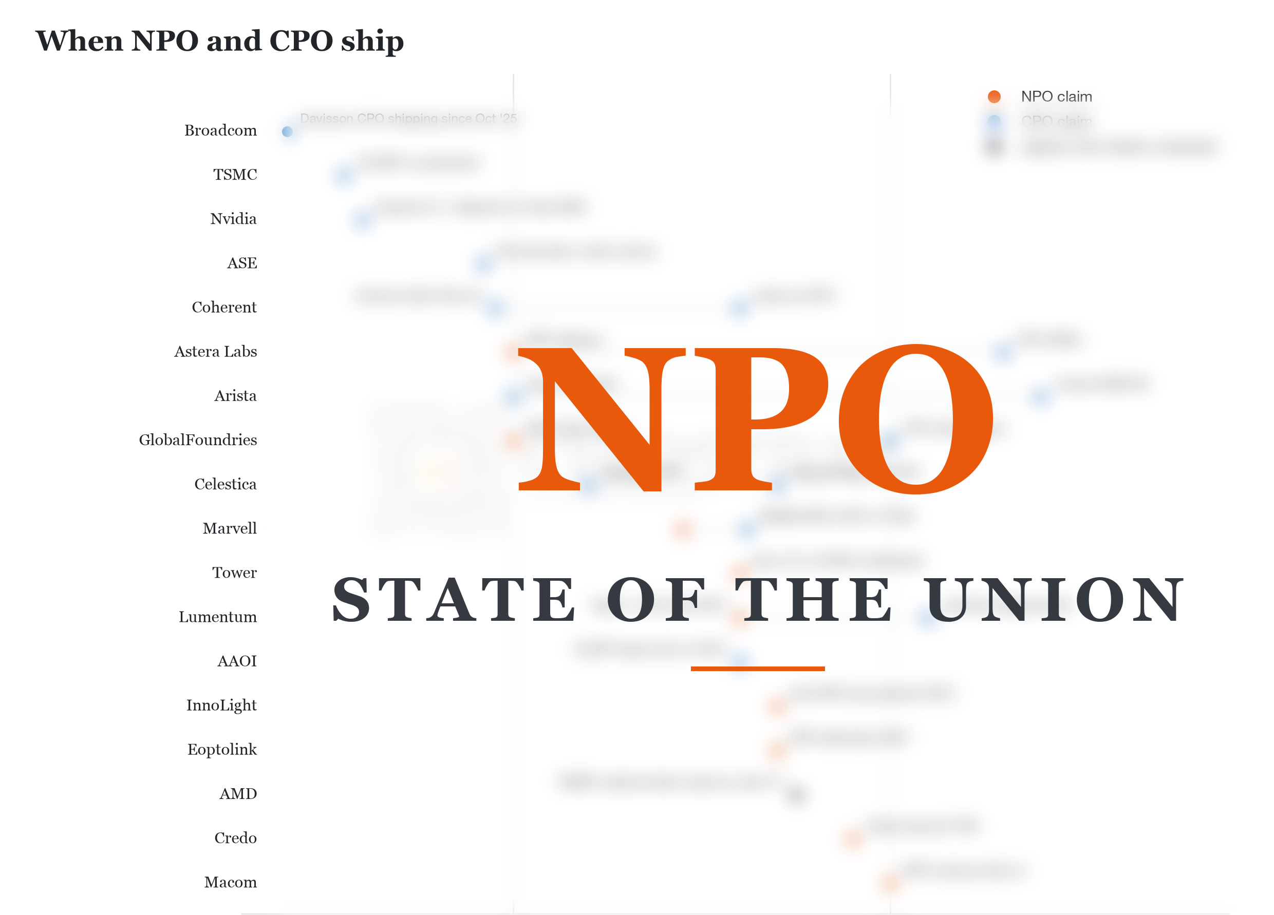 图01|原文配图(Chipstrat)
It’s coming up a lot on earnings calls. From GlobalFoundries:
Karl Ackerman, BNP Paribas: For my follow-up, if I may, could you discuss what portion of those 7 customers on your SCALE platform are working on NPO or near-packaged optics – and I guess how should we think about the timing of your NPO opportunity?
Tim Breen, GF CEO: Yes. Maybe just to take a step back, and I think there’s obviously a year ago, the industry wasn’t talking a lot about NPO – now it’s talking a lot about it.
Let me remind newer folks quick about NPO.
Today’s pluggable transceiver is the industry’s workhorse, but it burns a lot of power. The module connects at the switch faceplate (far from the switch chip), so a long copper trace on the board is needed. High-frequency signals over copper degrade, so a power-hungry digital signal processor (DSP) sits in the transceiver, cleaning up and retiming signals in both directions, transmit and receive.
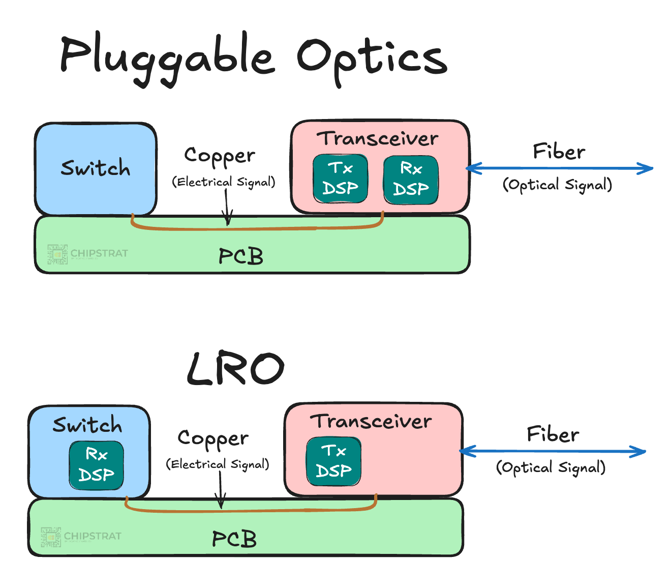 图02|原文配图(Chipstrat)
Linear optics such as LRO above give that cleanup work to the switch ASIC’s own SerDes. The transceiver can shed the DSP silicon (LRO sheds the receive half; LPO sheds all of it), and the power spent per transmitted bit drops.
Co-packaged optics take this to the logical conclusion and move the optical engine onto the chip’s own package.
NPO is the middle step. The optical engine moves onto the board a few centimeters from the chip, into a socket, but remains outside the package:
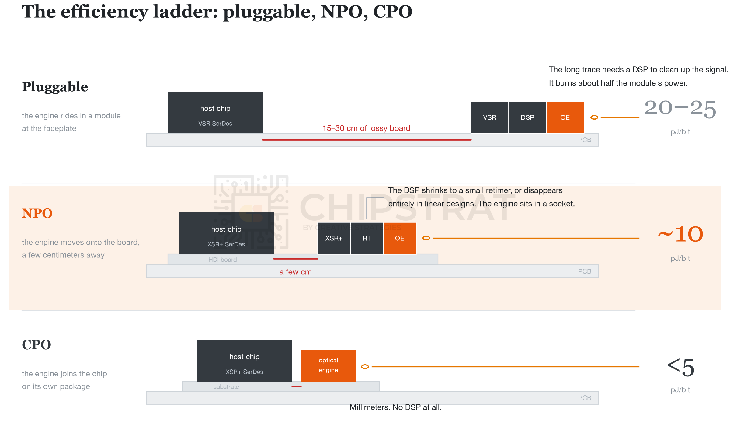 图03|原文配图(Chipstrat)
A nice two min video about this from my chat with Tom Barber:
(嵌入 Twitter 内容:Why are data centers moving from pluggables to co-packaged optics (CPO)? It’s a ladder of efficiency. • Pluggable: 20-25 pJ/bit (35dB loss) • NPO: ~10 pJ/bit (15-20dB loss) • CPO: <5 pJ/bit (<6dB loss) GlobalFoundries’ Thomas Barber on the physics driving the change.)
So “What is NPO?” is one of the five Ws, and now you might now be wondering about the other four Ws:
- WHEN NPO?
- WHERE NPO?
- WHO NPO?
- WHY NPO?
Well, more context.
Remember that the CPO switches in the news like Nvidia’s Quantum-X and Broadcom’s Davisson are CPO used in scale-out. And a quick reminder that scale-out doesn’t simply mean “rack-to-rack” and scale-up doesn’t simply mean “within a rack” as lots of folks tend to say online.
GPUs/XPUs/AI ASICs want to access each other’s memory so fast that the remote memory feels like their own. Accelerators on the same “scale-up domain” can do just that. They wish they had more HBM, but for now it’s just you get whatever is attached to your board and that’s it, so the hack is to access your neighbors as if it was your own. This landscape will change with HBM pooling btw, but that’s a topic for another day.
If accelerators aren’t on the same scale-up domain, then they communicate over the scale-out network.
Scale-up has historically lived within a server node first (e.g. just 8 GPUs in a scale-up domain) then within a rack (72 GPU domain). But the scale-up domain can span neighboring racks too! NVL576 connects eight racks of 72 Rubin Ultra GPUs into a single NVLink domain. We even see Kyber rack NVL1152 taking it to eight racks of 144 GPUs, with optical links between racks.
So the first CPO products are switches on the scale-out network. Not GPUs. The optical engine moves onto the switch substrate, and nothing changes on the GPU side; the endpoints still run pluggables and copper. This is just like the images above where the O/E is moving closer to switch ASIC.
OK, with that in mind, back to what the industry is saying about when, where, who and why.
We can see a shift in language from various industry participants; for example, back in February, Macom CEO Stephen Daly positioned Macom’s products as “optimized for co-packaged and highly integrated architectures, like CPO and NPO”. Ah ok, both NPO and CPO are a-comin’
In May the prepared remarks carried the same script line in different words, and it was the only CPO mention in the call. By August, the line read “highly integrated architectures like NPO and XPO”. What? Where is CPO? And XPO?! And that call also mentioned NPO nine times. Macom now talks about NPO and XPO, not CPO.
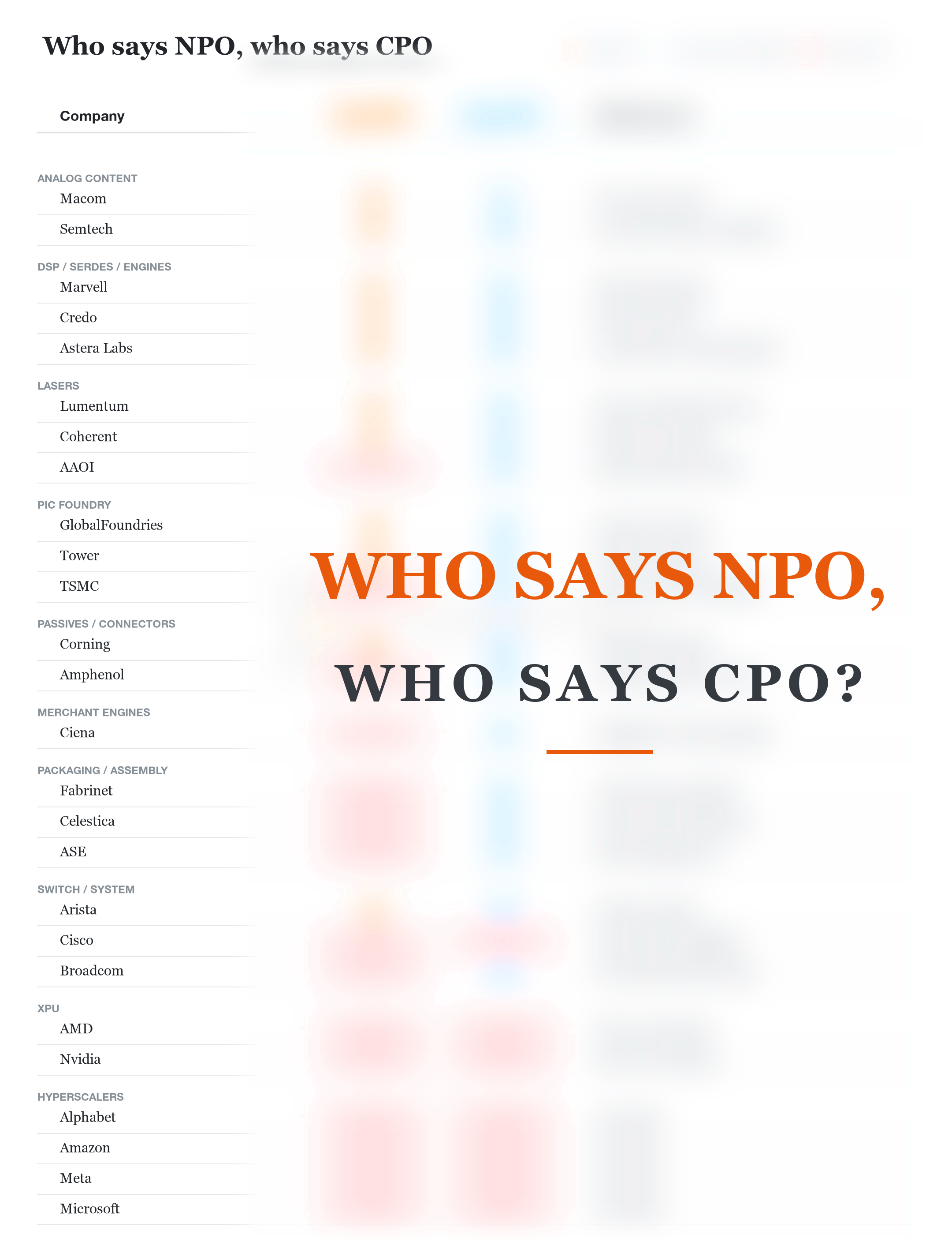 图04|原文配图(Chipstrat)
This raises follow-on questions.
- When is NPO ramping? And why didn’t this NPO-before-CPO come up sooner?
- Does NPO push CPO back entirely, or only in certain sockets?
- Who benefits from NPO? Who doesn’t?
- How much of the “CPO” shipping today is actually NPO? Is marketing at hand here?
- Is NPO accretive or cannibalistic? For whom?
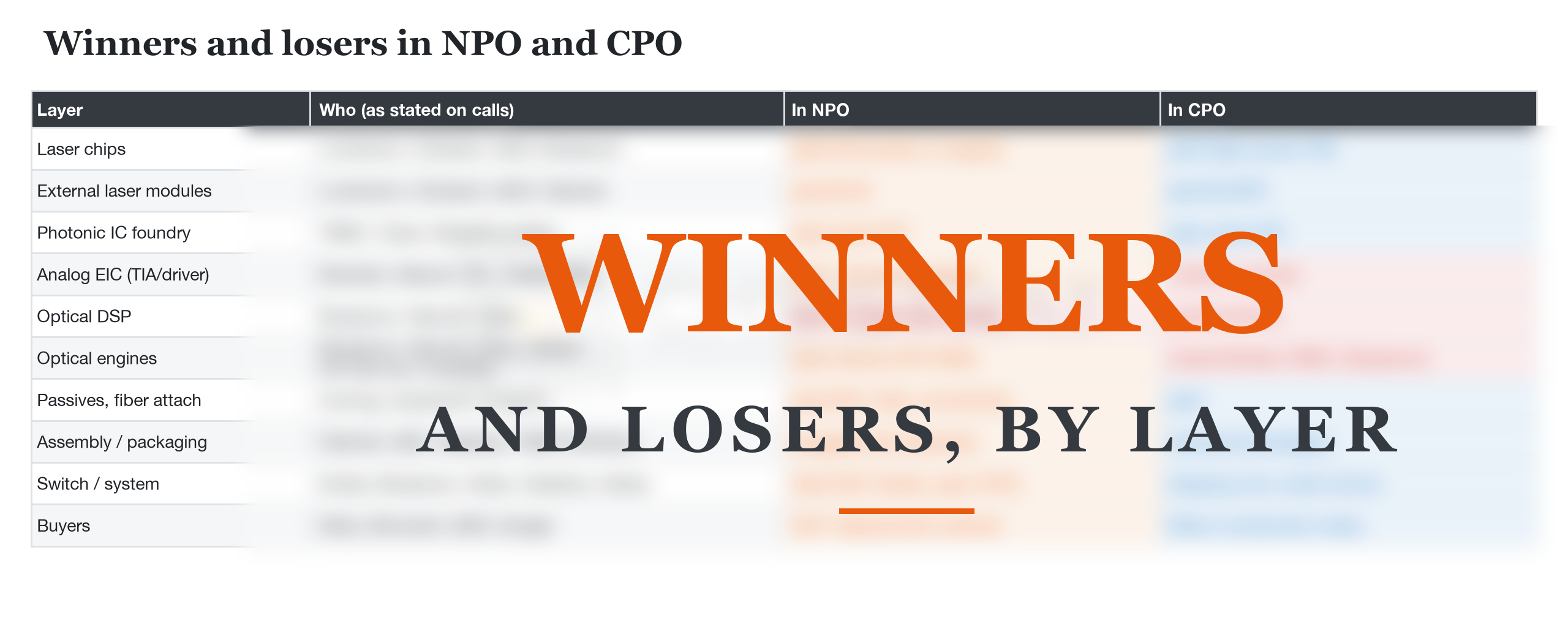 图05|原文配图(Chipstrat)
We’ll answer those below for subscribers.
We’ll also unpack the related MSAs and what they tell us.
We’ll touch on many companies including GlobalFoundries, TSMC, Tower, Lumentum, Coherent, AAOI, Macom, Semtech, Credo, Astera Labs, Marvell, Nvidia, AMD, Broadcom, Arista, Ciena, ASE, Celestica, Fabrinet, InnoLight, Eoptolink, HG Genuine.
(以下内容位于原文付费墙之后,未包含在本文转载范围内)
第二部分:解析(深度解读)
核心论点摘要
Chipstrat 这篇文章捕捉到 2026 年财报季最重要的措辞变化:NPO(近封装光学)已经从行业暗语变成了财报电话会的正式词汇。三个证据链:
- GlobalFoundries CEO 亲口确认:「一年前行业还不怎么谈 NPO,现在谈得很多了」——GF 的 Fotonix/SiPho 平台正在承接 NPO 光引擎的代工需求。
- Macom 的 CPO 措辞消失:2 月还是「CPO 和 NPO」,8 月变成「NPO 和 XPO」,且单场电话会提到 NPO 九次。模拟器件厂商的产品叙事已经完成切换。
- 能效阶梯的物理事实(GF Tom Barber 视频数据):可插拔 20-25 pJ/bit(35dB 损耗)→ NPO ~10 pJ/bit(15-20dB)→ CPO <5 pJ/bit(<6dB)。NPO 拿到了大约一半的 CPO 收益,但只需要一小部分工程代价。
关键概念解读
- 五个 W 的框架:NPO 是「光引擎搬到板上、距芯片几厘米、可插拔插座化、但仍在封装之外」。它是 DSP 可插拔(现状)与 CPO(终局)之间的中间台阶——比可插拔先进,比 CPO 保守。
- scale-out 与 scale-up 的澄清(作者特意纠正网络流行误读):第一代 CPO 产品(Quantum-X、Davisson)是 scale-out 交换机上的 CPO,GPU 端不受影响;scale-up CPO 要等 Feynman 世代。NVL576 已把 scale-up 域扩展到 8 机架,Kyber NVL1152 更是机架间走光互连——这正是 NPO 的用武之地。
- Macom 措辞切换的信号价值:模拟/PHY 器件商离系统设计最近,他们停止说 CPO 而改说 NPO+XPO,通常意味着客户实际下单的形态已经变了。
分层拆解表
| 光互连形态 | 每比特能耗 | 通道损耗 | 工程代价 | 商业成熟度 |
|---|---|---|---|---|
| 可插拔模块(DSP) | 20-25 pJ/bit | 35dB | 最低(现网存量) | 完全成熟 |
| LPO/LRO 线性直驱 | 中 | 中 | 去掉 DSP,依赖交换机 SerDes | 早期放量 |
| NPO 近封装 | ~10 pJ/bit | 15-20dB | 光引擎上板+插座化,免动封装 | 当前叙事主角 |
| CPO 共封装 | <5 pJ/bit | <6dB | 良率/散热/可维修性全要重做 | 交换机侧首发 |
技术趋势判断
NPO 的本质是把 CPO 的收益曲线切成两段收割:先用插座化、模块化的近封装形态拿到一半能效收益(且不碰先进封装良率),等混合键合、ELS、光引擎可靠性全部成熟后再进封装。对供应链而言,这意味着光引擎、SiPho、TIA/driver、激光器、光纤连接的需求被提前了,而不是被替代。本站此前对 CPO 规模化条件的分析见《What Will It Take to Deploy CPO at Scale》,对 NPO/CPO 财报解读另见《Optical Illusion: CPO is Dead, Long Live NPO》与《July NPO/CPO Update》。
风险提示
原文的受益公司名单与 MSA 分析在付费墙之后,本文未转载,请勿基于截断内容做完整推断;NPO 与 CPO 的边界本身仍在漂移(部分厂商把 NPO 产品也宣传为「CPO 家族」),存在营销口径混肴风险。本文不构成投资建议。