Hot Chips 2026: Tuning into Memory Vibes — 存储三巨头同台对比
Vik's Newsletter 逐家点评 Hot Chips 2026 存储三巨头:Micron 平淡、三星凭逻辑工艺 base die 讲出三阶段路线图、SK hynix 直面 MR-MUF 优势在混合键合时代终结的问题。
来源:Vik’s Newsletter — Hot Chips 2026: Tuning into Memory Vibes — Micron, Samsung, SK Hynix. 原文链接:https://www.viksnewsletter.com/p/hot-chips-2026-tuning-into-memory 原文发布日:2026-08-24 | 作者:Vik’s Newsletter(SemiExponent) 说明:本文为英文原文全文转载(免费文章),附中文深度解读。解读部分为整理归纳,不代表原作者观点。
第一部分:正文(Original Article)
This is my first time attending the Hot Chips conference and the overall vibe was a small, tight knit conference with a lot of interactions. No parallel tracks running and continuously having to choose what to attend. The talks from big companies, especially the big three, were pretty detailed; think of it as a collection of heavily technical keynotes.
In this quick note, we will cover presentations from the big three memory players. These are only initial captures from my notes. There is a lot to think about regarding implications and what the proceedings mean for the roadmap, but that takes time.
Contents:
- Micron
- Samsung
- SK Hynix
Micron: We’re so important, we make HBM
This talk was definitely the most unimpressive of the big three, so let’s get it out of the way first. Most of the talk was about the regular culprits like the memory wall, standard roofline curves, and how stacking enables high memory bandwidth. For an audience tuned to AI (aka, most of the lecture hall), this is not news. Only a few things stood out, and we’ll mention those quickly.
The slide below was one of the more informative comparison slides between the different HBM generations. Most tables like these only cover the overall memory bandwidth, capacity, and stack height. This one compares number of channels, pseudo-channels, burst length, processor controller (PC) width, and bitrate per lane, in addition to the usual numbers. The level of detail is admirable. We will not get into what they all mean here, but the main thing to note is that HBM has a lot more technical metrics that matter to performance than meets the eye on marketing slides.
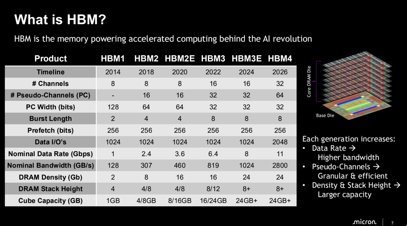 图01|HBM 各世代规格对比(Micron 演讲幻灯片)
We have discussed why HBM is so hard to manufacture in an earlier post. Of note was the fact that HBM is the 2nd most important root cause of training-run interruptions, apart from the GPU being faulty itself. Software and networking were #3 and #4, respectively. You can read the whole study here.
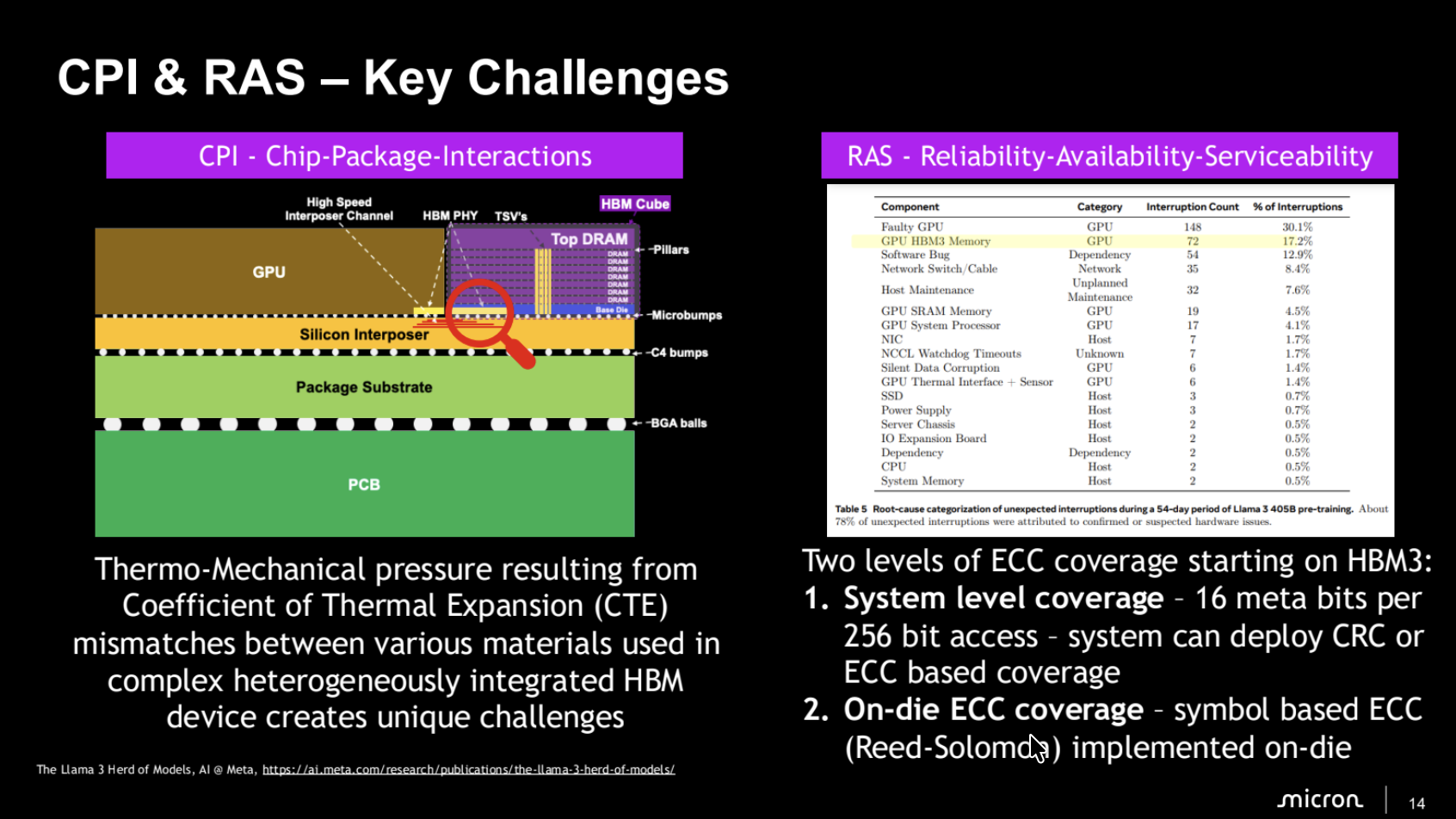 图02|训练中断根因分析:HBM 是仅次于 GPU 故障的第二大因素
Notably a few things were absent from Micron’s talk:
- Scaling to higher stacks (16-hi/20-hi) and the future roadmap for hybrid bonding.
- Any mention of custom base die, and why that is important going forward.
- Cooling solutions as HBM lane rates get faster.
At the surface, this might seem like a downside. Given the recent rumors of HBM stack height downgrades, it is questionable if some of these are even required in the future. Except custom base die. That is important, and will continue to exist in logic node implementations — I argue even in lower stack height implementations. Samsung will explain why next.
Samsung: Custom base die on logic nodes because we can
I enjoyed Samsung’s talk so much that I live tweeted the key takeaways from the conference. We’ll briefly expand on these topics here.
Interestingly, they had some charts showing how HBM5 would evolve in terms of spec. Even though nothing is set in stone, it’s fun to see charts up and to the right.
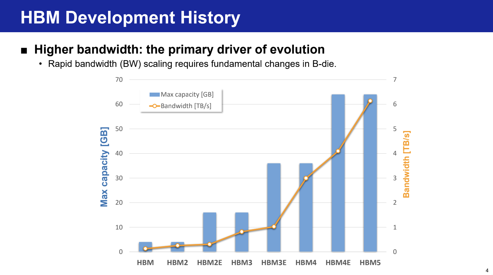 图03|Samsung 展示的 HBM5 规格愿景
HBM5 with a capacity of 60GB and 6 TB/s bandwidth would be nice. Let’s calculate some numbers here. 6 TB/s with 2,048 lanes would mean 23.5 Gbps per pin. We are currently at 16 Gbps state-of-the-art, and that is a significant step up that is likely possible with an advanced logic node. For 60 GB capacity with 3 GB per die, that would put the stack height at 20 high.
In a separate slide, Samsung confirms that HBM4E is running at 16 Gbps per pin. HBM5 calculations we did above are also validated in the chart below.
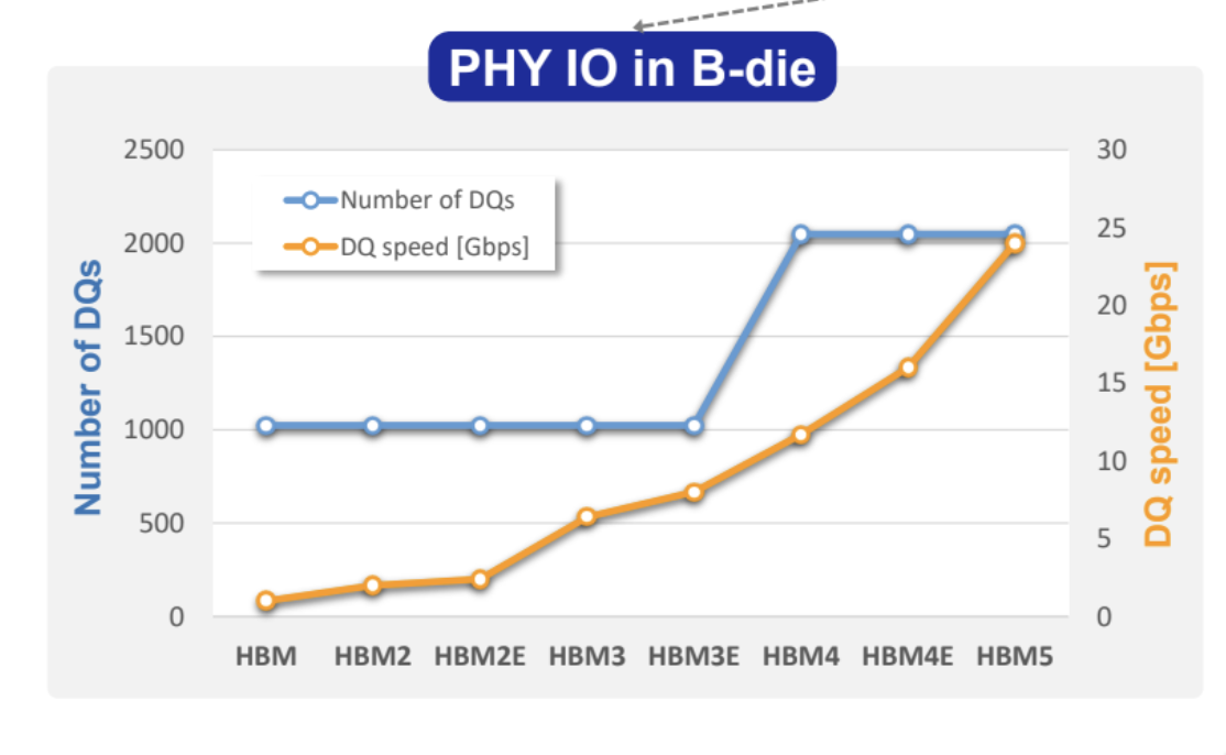 图04|Samsung 确认 HBM4E 跑在 16 Gbps/pin,并验证 HBM5 计算
Samsung’s clear advantage is that they have a logic node in-house unlike Micron and SK Hynix who need to partner with somebody to get it. They were sure to play up their advantages here by explaining how custom base die is important going forward. Samsung is using 1c node for memory and 4nm node for logic. It results in a significant power reduction in the base die. The slide below is a silent dig at Micron who used DRAM nodes for logic die in HBM4.
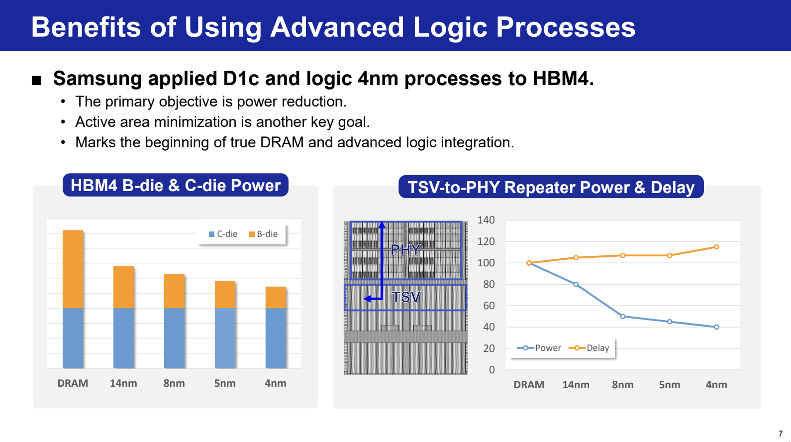 图05|Samsung:1c 存储节点 + 4nm 逻辑节点带来 base die 显著降功耗
What was even better was how Samsung broke up the roadmap into three clear phases. We’ll cover each one.
Phase 1: The Low Hanging Fruit
When there is a logic node in the base die, the physical footprint of the HBM PHY block reduces in area and also becomes more energy efficient. This means that the block that works on die-to-die connects between HBM and XPU gets smaller. This has two positives:
- Increases the area in XPU for more compute
- Increases available area in HBM base die for more advanced functions.
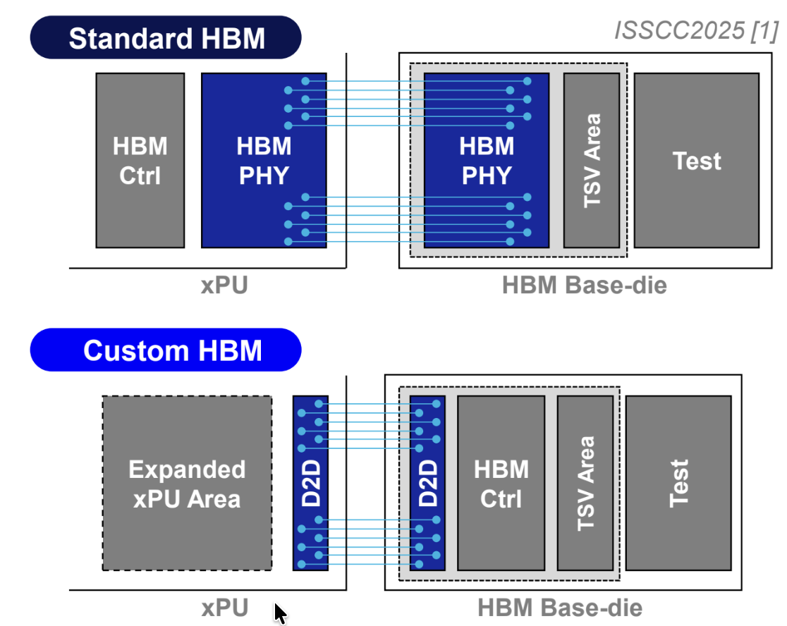 图06|逻辑工艺 base die 使 HBM PHY 面积缩减、能效提升
The downside of the shrinking size is more thermal density in these regions. It was interesting that they provided actual sizes of their PHY blocks in various HBM generations.
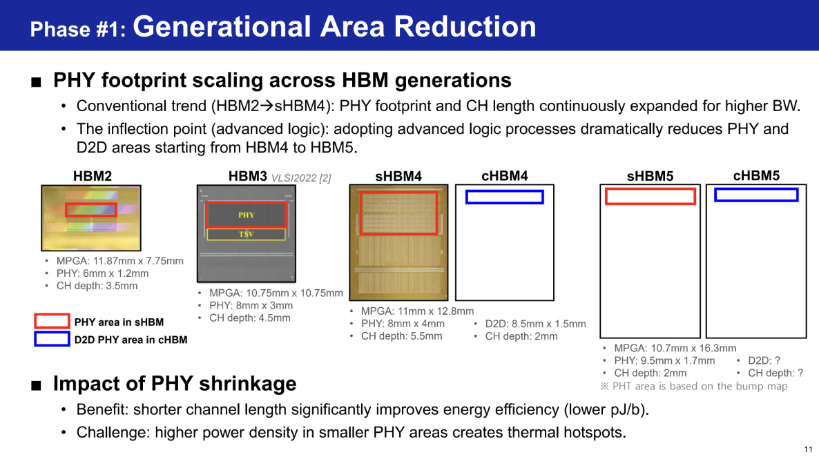 图07|Samsung 公布各 HBM 世代 PHY 块的实际尺寸
Samsung also mentioned that they were not inclined to use UCIe for their D2D link because of larger size and poorer energy per bit. They said that their custom PHY implementation was better in performance. When moving to HBM5, they showed the concept of an integrated Heat Path Block (HPB) to cool the D2D PHY region.
The next big advantage is memory controller offloading which can be moved from the XPU to the custom base die. This reclaims area in the XPU die which can then be used to drive up flops.
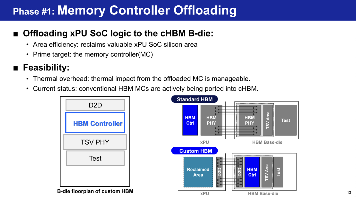 图08|内存控制器从 XPU 卸载到 base die,腾出算力面积
The new benefit of having a logic node in the base die is that you can have SRAM. If a particular cell in the DRAM stack is broken, the information in that cell can instead be stored in SRAM and the memory controller will look up SRAM for those cells instead of failed DRAM cells. Think of SRAM as a spare notebook which acts as a scratchpad to hold data that could otherwise not be held in defective DRAM cells.
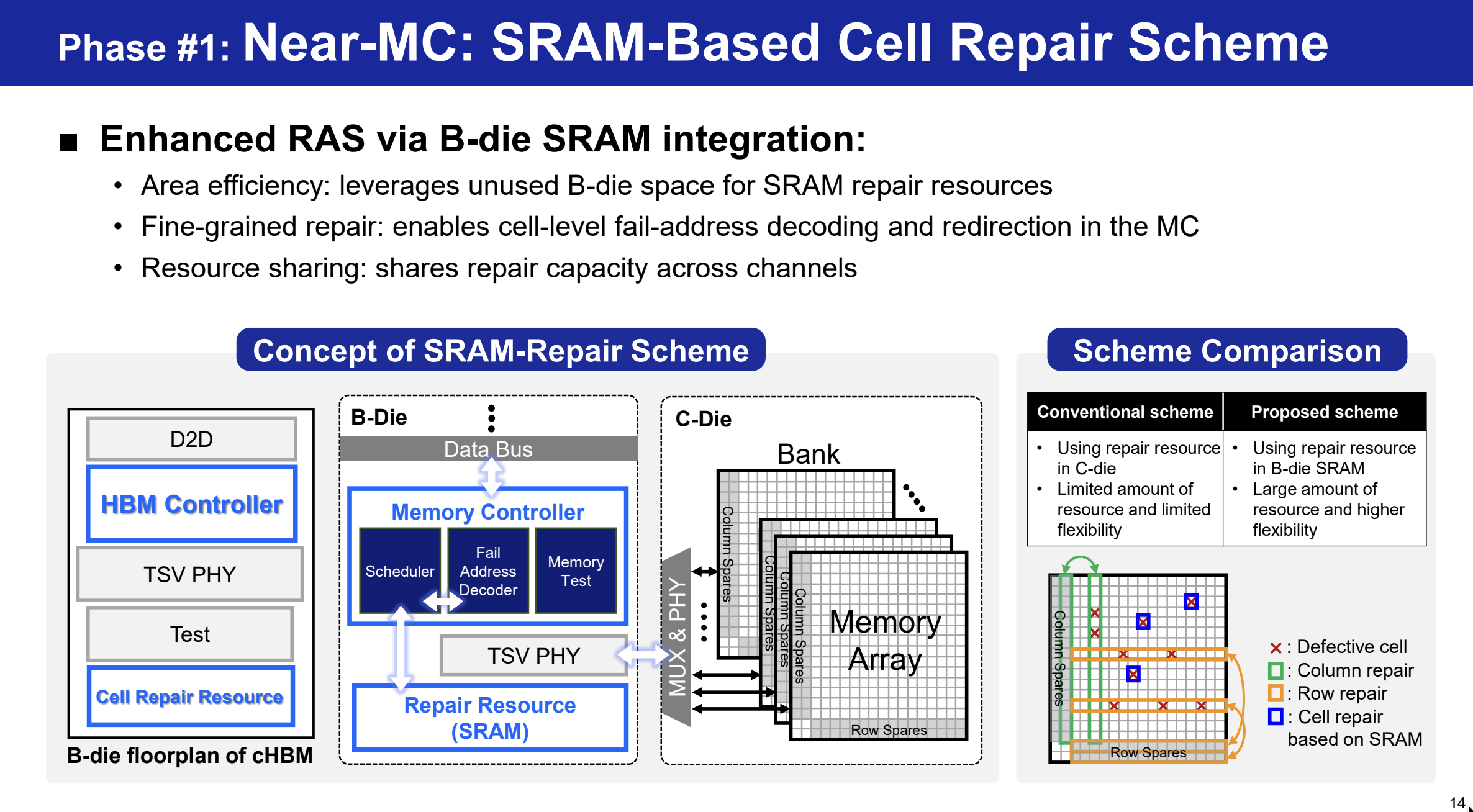 图09|base die 上的 SRAM 充当坏 cell 的冗余存储
Phase 2: RAS, Test, Extension, Processing
The use of a logic node for base die means that silicon area used for a lot of these functions is smaller if the transistors are smaller. The extra space available is useful for a few things like Repairability-Availability-Serviceability (RAS), testing, and collecting telemetry data about the health/status of the HBM memory stack. HBM telemetry data will be very useful given that it is the #2 thing to kill a training run.
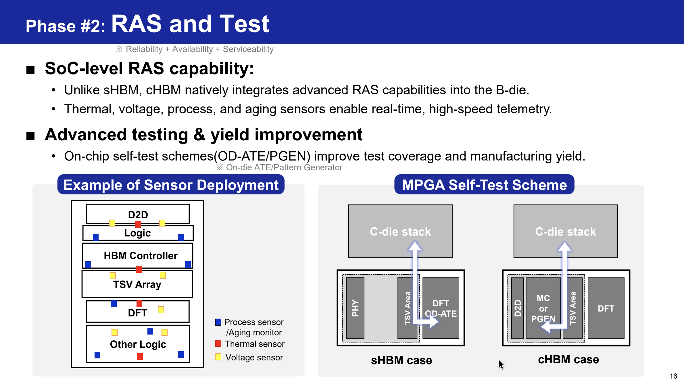 图10|RAS、测试与 HBM 健康遥测
If there is even more silicon area left over, then one can build another memory extension controller to connect another HBM stack behind the first one or put in a DRAM chip to extend memory.
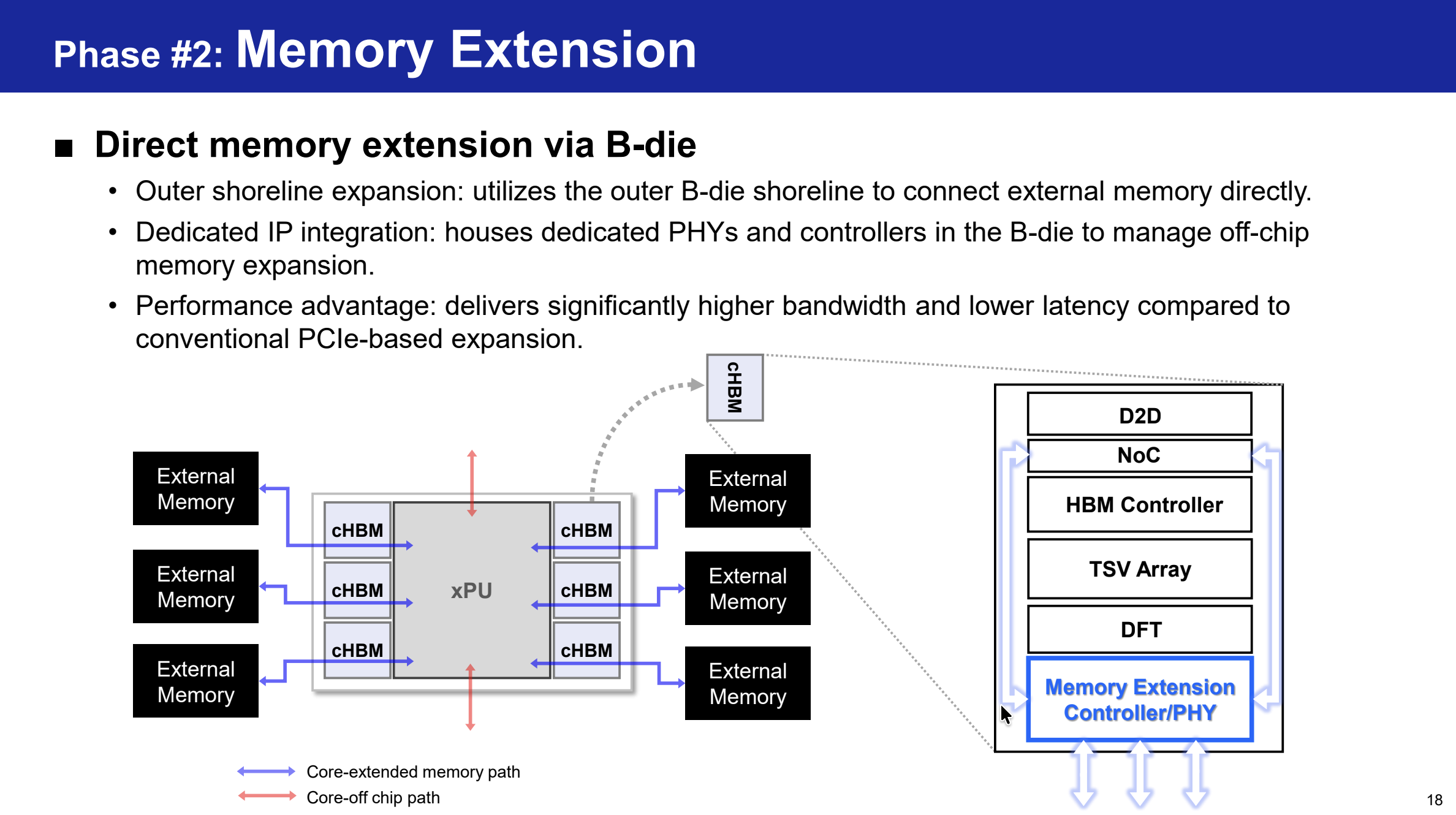 图11|内存扩展控制器:串联第二个 HBM 堆栈或 DRAM
Finally, if logic transistors are available, then why not throw in some compute within the base die too? The benefit is that some compute like matrix compression or encoding can be done on the logic die without ever leaving this base die. This has latency and efficiency advantages.
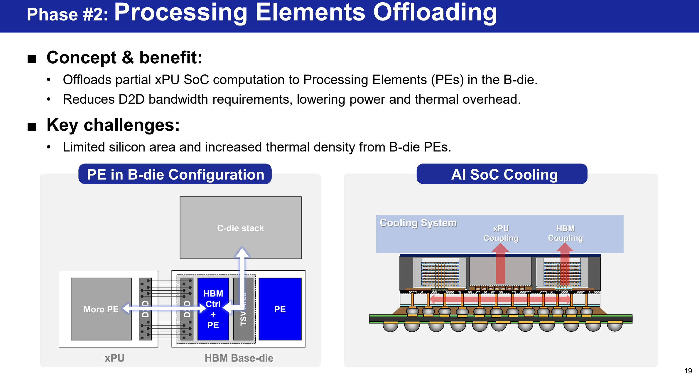 图12|在 base die 内做矩阵压缩/编码等计算
If that all works out, then one can in theory construct the nice little accelerator on the bottom right. It is easy to draw block diagrams like this, and conceptually nice to imagine, but its real performance benefits are questionable.
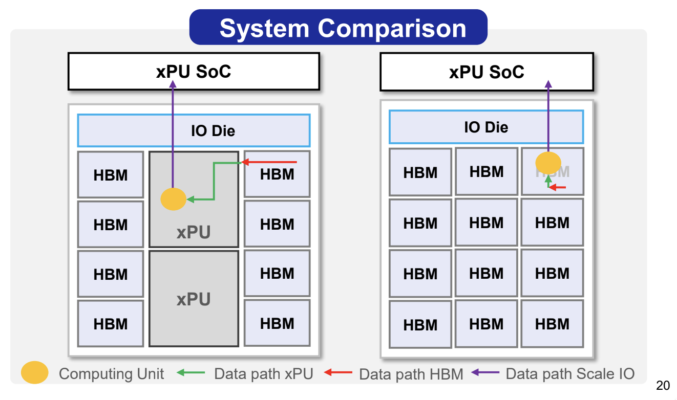 图13|理论上可在 base die 上构建的微型加速器
Phase 3: Going vertical
The final phase is use the custom base die + HBM and stack it on top of the logic die. The distance between compute and memory is short, and thus bits need to be shuffled across much shorter distances which gives power efficiency benefits and increased memory bandwidth due to the ability to use more parallel data paths across the chip area rather than just the beach front.
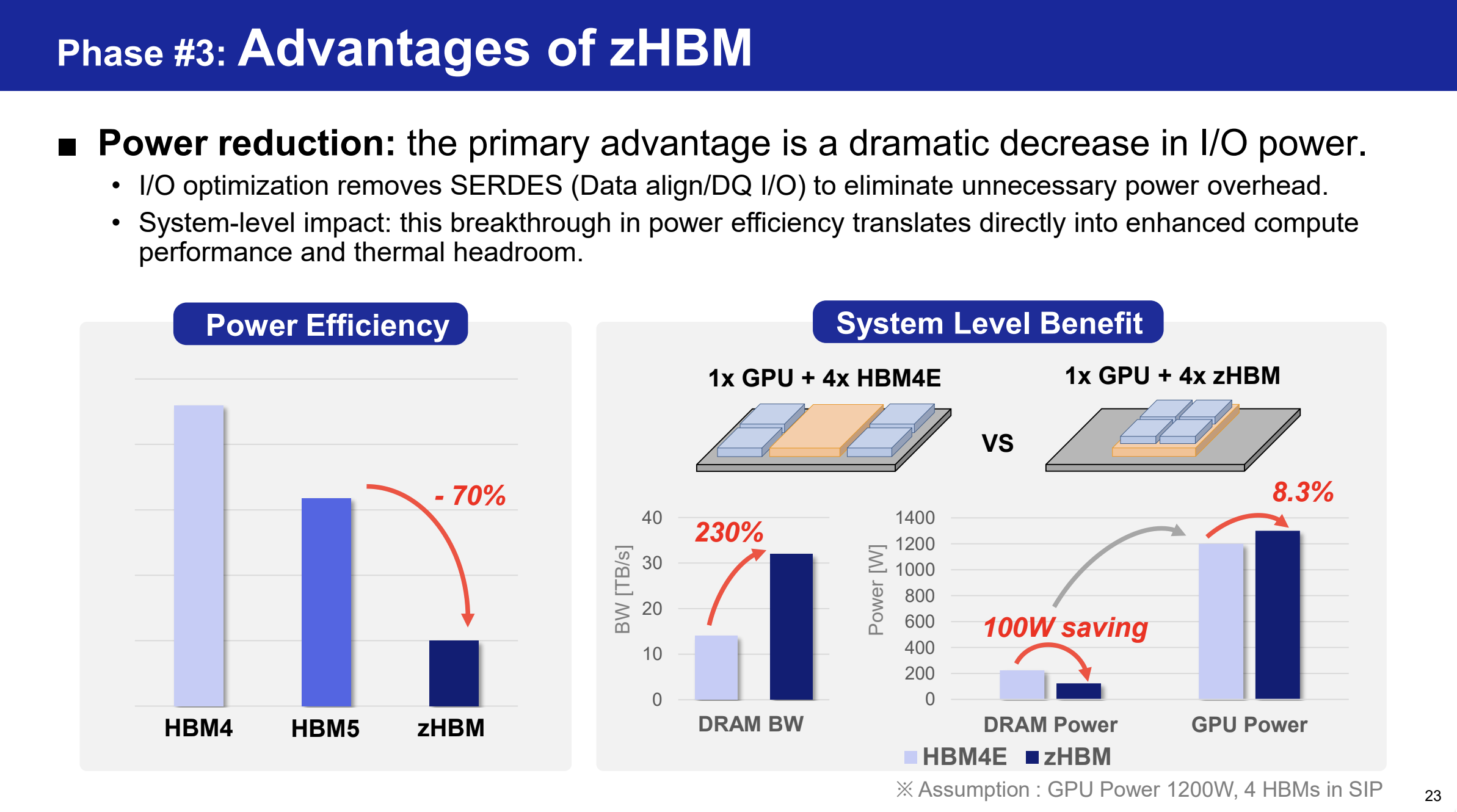 图14|Phase 3:HBM 堆叠到逻辑 die 之上
None of this is easy, but it is important for a company to have a roadmap ahead to improve technology. It proves that they have a path to an improved product in the future, and that is good to see in a company. Whether the market is ready to uptake that product is a different argument.
SK Hynix: MR-MUF advantage ends with Hybrid Bonding
SK Hynix’s performance advantage in HBM has always been their use of Mass-Reflow Mold-UnderFill (MR-MUF) technique which provides them with a unique advantage over Thermo Compression Bonding (TCB) we have discussed in detail in the past on this newsletter.
The slide below from SK Hynix highlights this advantage.
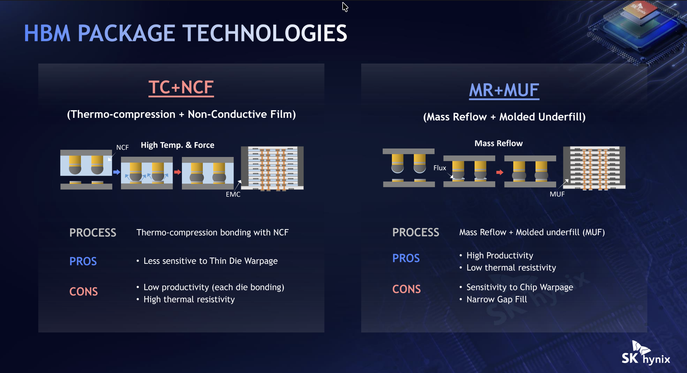 图15|SK hynix 强调 MR-MUF 相对 TCB 的优势
In fact, they have no problem in boldly claiming that MRMUF method works well for 16-high HBM, but that it would require 775 microns of overall stack height. The JEDEC spec was actually revised to support the larger height, so it does add up.
 图16|16-Hi MR-MUF 需要 775μm 总堆高,JEDEC 已为此修订标准
The question is: where does this MRMUF advantage go in the era of hybrid bonding, assuming that we ever get there and there is still a need for 20 high HBM.
Note that there is a chance that we will never get there because each DRAM wafer used for HBM purposes sucks up 3-4 times more wafers per bit. Given that the cost of memory alone is well above half the overall cost of a rack, the industry is trending to rely less on HBM if possible. This is where the news of de-specing HBM from 12-high to 8-high, and possibly even 4-high for some SKUs is coming from.
The slide below shows the benefit of MRMUF over TCB, where the thermal resistance is lower, and consequently results in better removal of heat from the middle regions of the stack. When hybrid bonding is used, the “secret sauce” of SK Hynix with MRMUF is no more, and everybody’s hybrid bonded HBM falls to the same level. If it comes down to this, it comes down to execution.
 图17|MR-MUF 热阻低于 TCB;混合键合时代这一优势将消失
The thermal management slide from SK Hynix below has an unusual comparison table that shows how Micron is the only one without an external heat removal solution. Samsung has Heat Block Path (HPB), and SK Hynix has Integrated Cooling Engine (ICE). Micron is just going to “improve circuit design” to get there. If that were the case, Samsung and SK Hynix would be doing it too instead of external cooling blocks.
 图18|散热方案对比:三星 HPB、SK hynix ICE,Micron 无外部散热方案
So it is either that Micron is behind on its next generation development, or has concluded that HBM will never reach those levels of stack height or per lane speeds that would require the development of advanced cooling solutions. It is not clear which one it is at the moment.
Lastly, there is an interesting mention on Intel’s EMIB on SK Hynix’s slide, noting that there are some customers using their memory with Intel’s packaging.
 图19|SK hynix 幻灯片罕见提及 Intel EMIB:已有客户用 Intel 封装搭配其 HBM
Final Thought
Even if stack heights do not go to 12, 16, or 20 in production environments, the use of custom base die on leading edge logic nodes is going to become important. It enables a higher data rate per pin, and we can see it being used even with lower stack heights due to all the advantages that Samsung pointed out.
The use of custom base die is, in a sense, decoupled from the stack height because it materially provides a plethora of advantages over a standard base die developed in a memory technology. In this regard, Samsung has the advantage in this playing field due to the availability of in-house advanced logic processes.
Lastly, I really love beautiful 3D renders of HBM sitting next to GPUs. SK Hynix’s look the best.
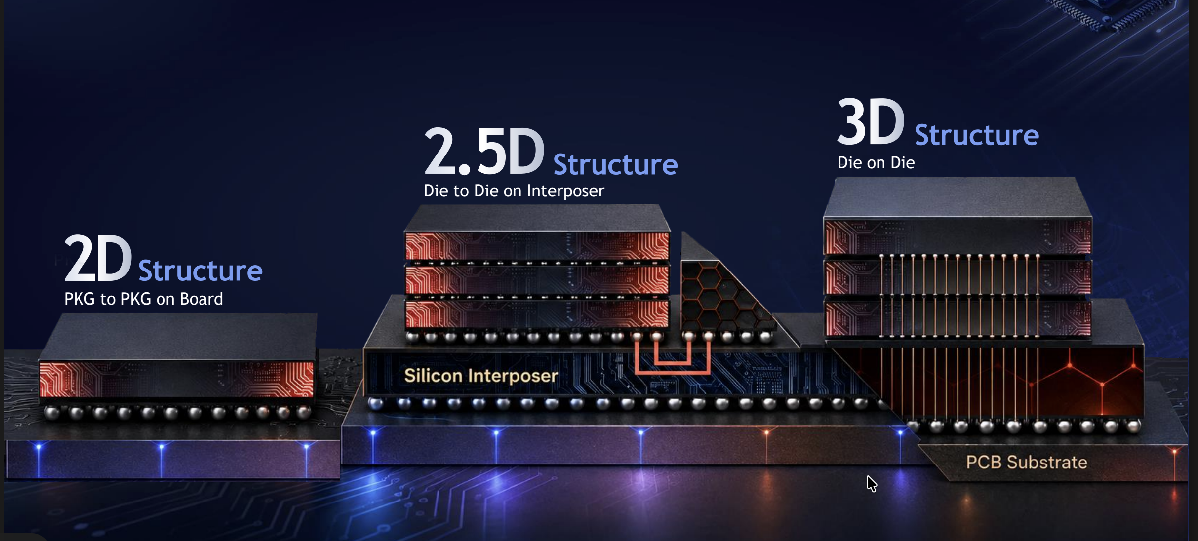 图20|SK hynix 的 HBM+GPU 3D 渲染
第二部分:解析(深度解读)
核心论点摘要
Vik 的现场笔记给出了 Hot Chips 2026 存储专场的三档评价:
- Micron:最无亮点。讲的还是 memory wall、roofline 曲线等陈词;且被点名缺席三个关键议题——16/20-Hi 与混合键合路线、定制 base die、散热方案。尤其散热:三星有 HPB、SK hynix 有 ICE,Micron 只说「改进电路设计」——要么落后,要么判断堆叠高度根本走不到那一步。
- Samsung:凭逻辑工艺讲出全场最佳。1c 存储 + 4nm 逻辑 base die 的三阶段路线图:Phase 1 PHY 面积缩减+内存控制器卸载+SRAM 冗余修复;Phase 2 RAS/遥测/内存扩展/base die 内计算;Phase 3 垂直堆叠到逻辑 die 上。HBM5 愿景:60GB、6TB/s、2048 lane 下 23.5Gbps/pin(当前 16Gbps)。
- SK hynix:直面自己的护城河倒计时。MR-MUF 在 16-Hi 仍成立(代价 775μm 堆高),但混合键合时代「秘方失效、人人平等」;Intel EMIB 出现在其幻灯片上——有客户已用 Intel 封装搭载 SK hynix HBM。
关键概念解读
- HBM5 的算术:6TB/s ÷ 2048 lane = 23.5Gbps/pin,相对当前 16Gbps 的跃升「很可能需要先进逻辑节点才能实现」——这句把 base die 逻辑工艺从可选项变成必选项。60GB(3GB/die)→ 20-Hi 堆叠。
- 「HBM 去规格化」的经济学根源:每 bit 的 HBM 要消耗 3-4 倍 DRAM 晶圆;内存成本已超过机架总成本一半 → 行业趋势是能少用就少用,12-Hi 降到 8-Hi 甚至 4-Hi 的传闻由此而来。堆高竞赛与成本约束在反向拉扯。
- base die 与堆高解耦:即使堆高不再上探,逻辑工艺 base die 的收益(PHY 面积、控制器卸载、SRAM 修复、遥测、内计算)依然成立——这是作者全文最重要的结构性判断。
- 训练中断根因:HBM 是仅次于 GPU 本身故障的第二大训练中断根因——base die 上的 RAS/遥测能力因此具备真金白银的价值。
分层拆解表
| 厂商 | 核心叙事 | 独有优势 | 暴露的短板 |
|---|---|---|---|
| Micron | 常规技术综述 | HBM 世代规格对比表(信息量大) | 无散热方案、无混合键合/堆高路线、base die 缺位 |
| Samsung | 逻辑工艺 base die 三阶段 | 自有 4nm 逻辑产线(Micron/SK 需外协) | 概念图多于实测;20-Hi 市场需求存疑 |
| SK hynix | MR-MUF 现阶段优势 + 坦承混合键合后归零 | 16-Hi 量产执行力、EMIB 客户背书 | 优势有时限;775μm 堆高挤占系统设计空间 |
技术趋势判断
本场演讲合并读出的产业信号:HBM 竞争的决胜变量正从「堆叠工艺」转移到「逻辑工艺 base die」。三星是唯一逻辑+存储都在手里的玩家(作者原话:because we can);SK hynix 与台积电/Intel 的绑定因此更加性命攸关——这与本站《SK hynix 先进封装路线图》(EMIB/CoWoS 并列出现、power TSV 遍布)互为印证。内存架构层面的更大图景(zHBM、PIM、CXL、内存池化)见《The Battle for the Next AI Memory》。
风险提示
作者的点评基于现场速记,自称「initial captures」;HBM5 规格为三星单方愿景(nothing is set in stone);「HBM 降规格」传闻尚未获原厂确认;base die 内计算的性能收益被作者自己标注「存疑」。本文不构成投资建议。