Google's TPU Supply Chain — 中文解读
DataGravity 拆解谷歌 TPU 从自研 ASIC、代工、HBM、CoWoS 封装到光模块与整机的供应链骨架。
来源:DataGravity — Google’s TPU Supply Chain 原文链接:https://www.datagravity.dev/p/googles-tpu-supply-chain 原文发布日:2026-06-02 | 作者:DataGravity 说明:本文为英文原文全文转载,附中文结构化解读。原文以英文写就,未作翻译;解读部分为整理归纳,不代表原作者观点。
第一部分:正文(Original Article)
Google’s Tensor Processing Unit program is no longer a side project to keep GPU costs down. It is the structural foundation of how Google intends to own AI compute economics for the next decade. The signal most investors missed: in 2026, Alphabet conducted its first equity raise since its 2004 IPO , pulling in $80 billion — a move that only makes sense if the capital requirements of this infrastructure buildout exceed what operating cash flows can absorb. Alphabet spent $91.4B in capex in 2025 (up from $52.5B in 2024) and has committed $175–185B for 2026.
 图01|原文配图(DataGravity)
We first started writing about hyperscaler ASIC programs and the Google TPU back in early 2024. The ASIC programs have expanded massively since. This post maps every layer of the TPU supply chain: silicon design, fabrication, packaging, memory, optical interconnects, and system assembly — with the key beneficiaries at each layer.
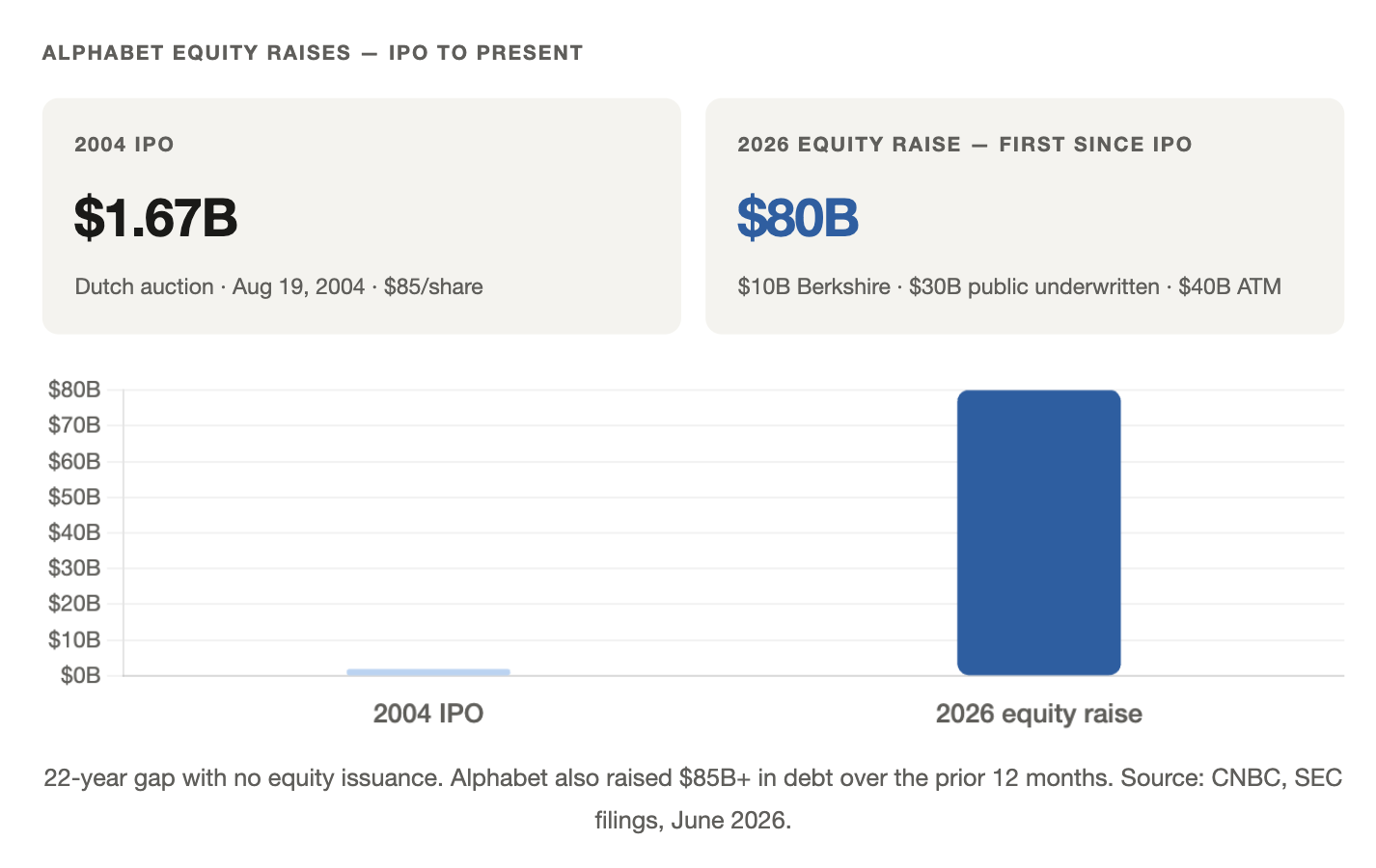 图02|原文配图(DataGravity)
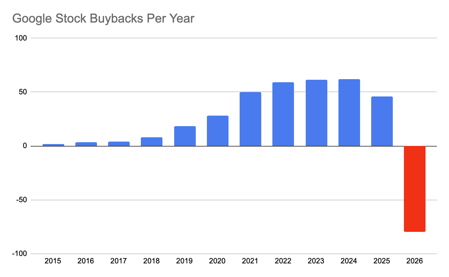 图03|原文配图(DataGravity)
The popular narrative is that Google does everything themselves. The reality? Their infrastructure relies on a quiet, but critical, ecosystem of hardware partners. The architecture is Google’s. The implementation is not.
These design partners feed into a five-layer supply chain extending from chip architecture through to server rack assembly across six countries.
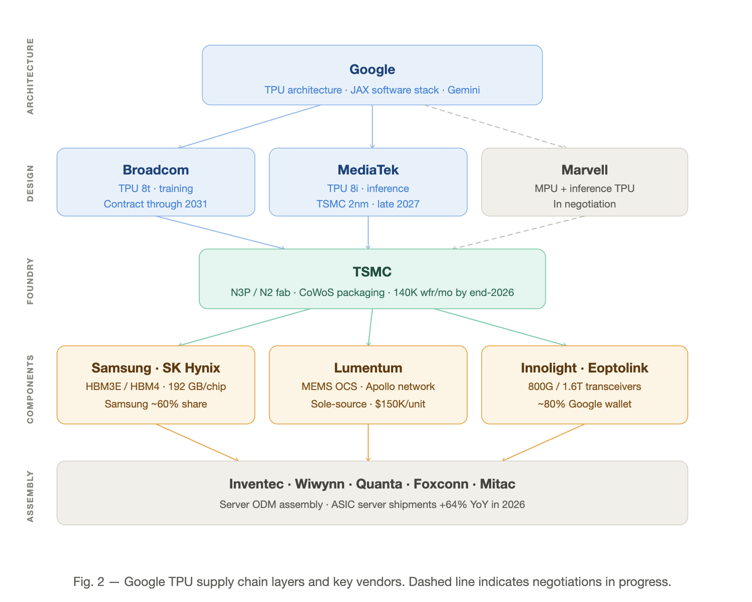 图04|原文配图(DataGravity)
Architecture: What Ironwood Actually Is
Before mapping the supply chain, the architecture matters. Google’s seventh-generation TPU — Ironwood (TPUv7) — represents a fundamental design break, and its choices determine who wins supply chain share.
Each chip delivers 4.6 petaFLOPS of dense FP8 — ahead of Nvidia’s B200 at 4.5 PFLOPS — with 192 GB of HBM3E at 7.4 TB/s bandwidth via eight stacks. Manufactured on TSMC N3P with CoWoS advanced packaging, Ironwood is a chiplet design with two dies connected via a 6x-speed die-to-die link. The defining architectural bet is the network: 9,216-chip superpods interconnected via a 3D Torus topology and Google’s Apollo Optical Circuit Switch (OCS) — an all-optical fabric where a single switch draws ~100W versus ~3,000W for traditional electronic switching. At pod scale, that delta is structural.
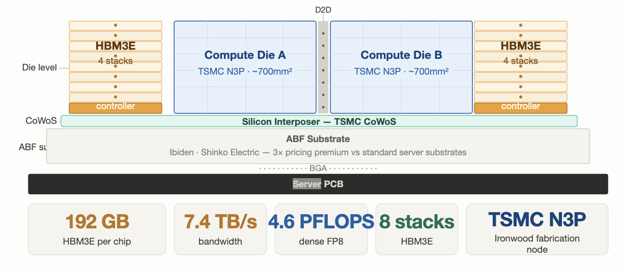 图05|原文配图(DataGravity)
2026 TPU shipment estimates span 3.3 million units on the supply-constrained end (DigiTimes Research, citing CoWoS packaging limits) to 4.6 million on the high end (Bank of America). The range reflects a genuine CoWoS allocation constraint, not demand uncertainty — Google’s order book is not the binding variable. ASIC server shipments overall are forecast to grow 64.2% in 2026 versus 43.8% for GPU servers, with Google accounting for the dominant share among hyperscalers.
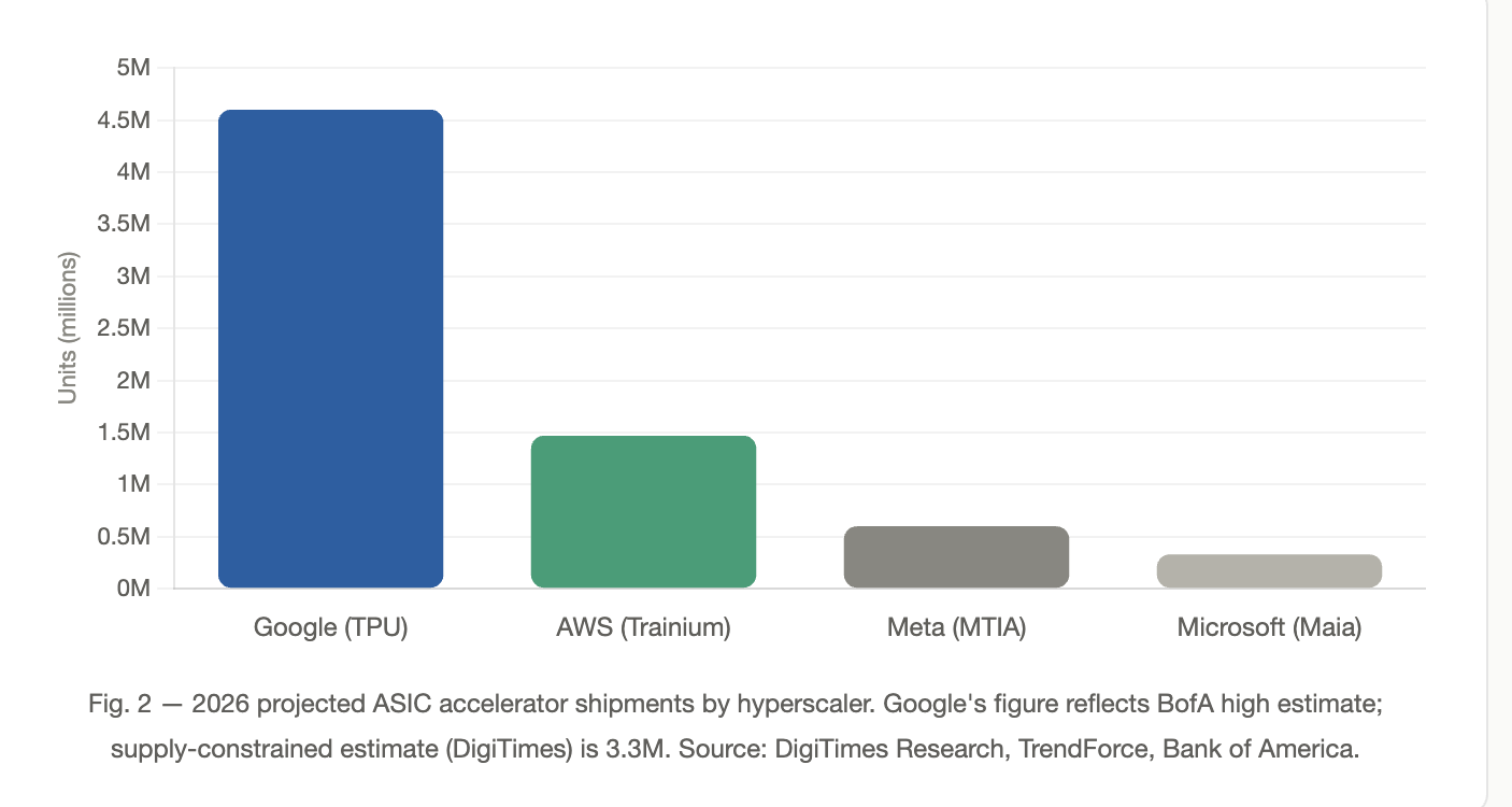 图06|原文配图(DataGravity)
2026 projected ASIC accelerator shipments by hyperscaler. Source: DigiTimes Research, TrendForce.
Silicon Design Partners
Google owns the TPU architecture and software stack. The implementation work is distributed across a growing set of ASIC design partners — all fabbing at TSMC — with deliberate competitive tension built in.
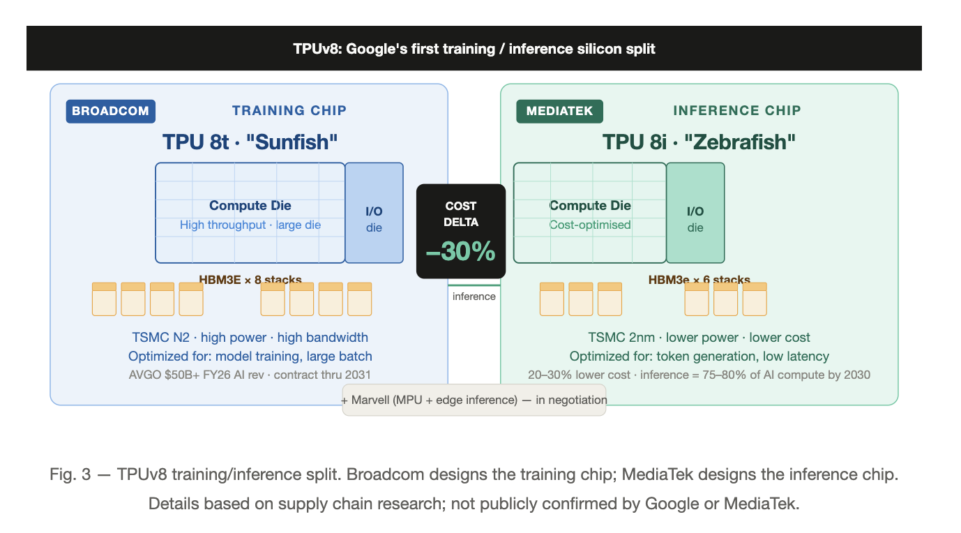 图07|原文配图(DataGravity)
Broadcom — primary design partner
Broadcom translates Google’s architecture into a manufacturable ASIC layout, contributes high-speed SerDes IP, handles power delivery, and coordinates CoWoS packaging with TSMC. The structural position is the story: the contract runs through 2031 , Broadcom carries a $73B AI backlog scheduled for delivery over the next 18 months, and the company holds >70% market share in custom AI accelerators globally. The financial trajectory follows from that position. Full-year FY2025 AI revenue reached $20B (+65% YoY) ; Q1 FY2026 came in at $8.4B (+106% YoY) , with Q2 guided to $10.7B. JPMorgan forecasts $50B+ for full-year FY2026 — ~150% growth. CEO Hock Tan has stated “line of sight to $100B in AI chip revenue in 2027,” with Google and Anthropic representing the dominant share.
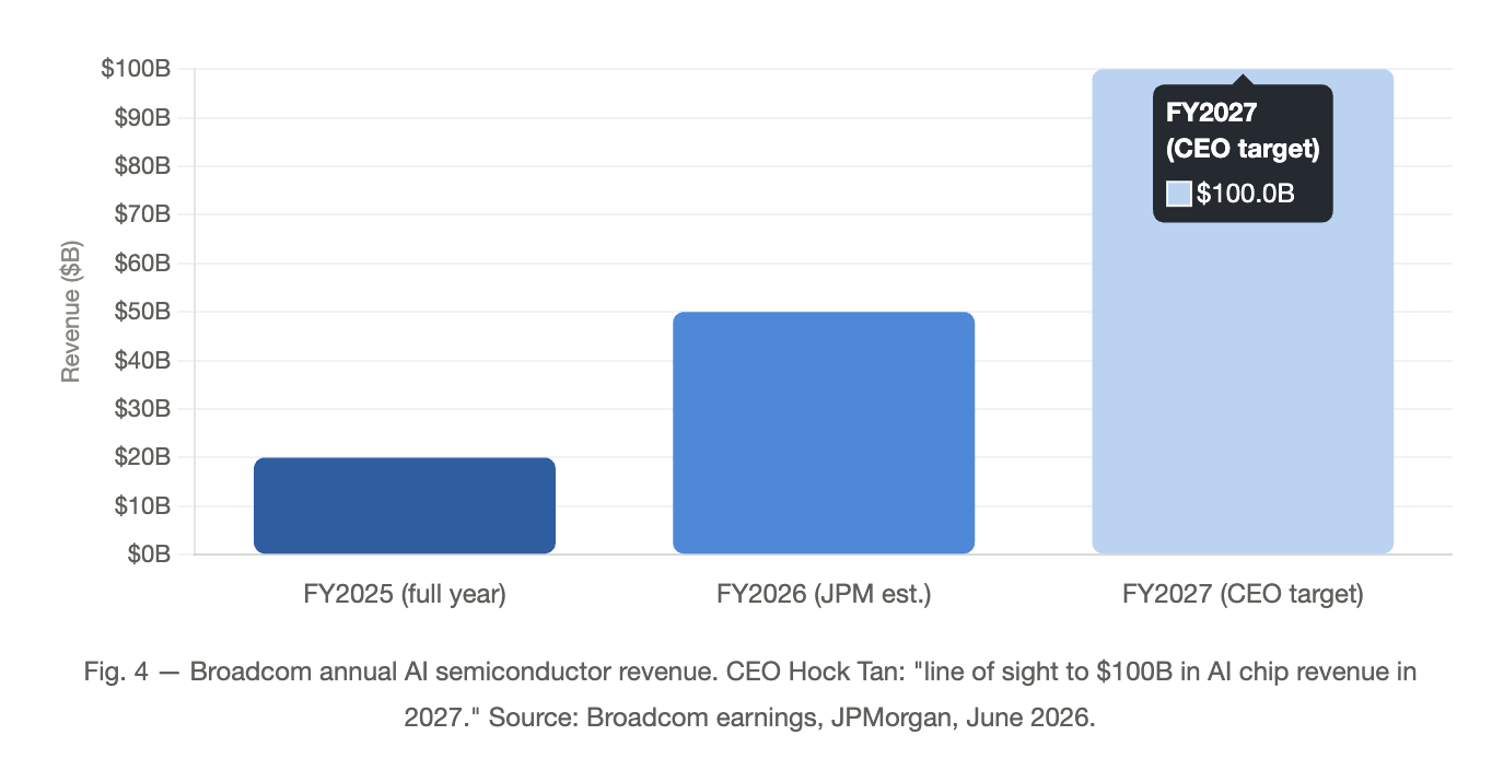 图08|原文配图(DataGravity)
MediaTek — inference design partner
TPUv8 splits training and inference at the silicon level. Based on supply chain research (neither Google nor MediaTek has made a public announcement), MediaTek is designing the TPU 8i (”Zebrafish”) — a single compute die plus one I/O die plus six HBM3e stacks, targeting TSMC 2nm in late 2027. The cost profile is the thesis: Zebrafish targets 20–30% lower cost than the training variant. As inference grows to 75–80% of all AI compute cycles by 2030 (per industry estimates), a purpose-built, cost-tuned inference die has durable demand. For MediaTek, it is the entry ticket into hyperscale custom silicon — a market TrendForce sizes at $118B by 2033.
Marvell — in negotiation
Google is in active discussions with Marvell for two chips: a memory processing unit and an inference-optimized TPU variant. No contract is signed as of mid-2026. Marvell’s custom silicon business runs at a $1.5B annual rate across 18 cloud-provider design wins. Adding Google would be transformative. The multi-partner strategy — Broadcom for training, MediaTek for inference, Marvell for edge inference and memory processing — creates pricing competition and eliminates single-source capacity risk.
Fabrication and Packaging
TSMC manufactures every Google TPU. Ironwood runs on N3P; TPUv8 targets N2, with tape-outs planned for 2026–2027. TSMC also handles CoWoS advanced packaging — the step integrating compute chiplets with HBM3e stacks. TSMC is targeting 140,000 CoWoS wafers per month by end-2026, a 4x expansion from early 2024. Even at that scale, CoWoS remains an allocation market — which is why supply chain researchers and Bank of America disagree on 2026 TPU volumes by more than a million units.
CoWoS packaging requires ultra-high-density ABF substrates. Ibiden and Shinko Electric dominate this layer. AI server substrates carry approximately 3x the pricing premium of standard server substrates due to layer count and routing complexity. New fab construction takes 2–3 years and hundreds of millions in capital — supply cannot respond quickly to demand.
High-Bandwidth Memory
Ironwood’s 192 GB per chip, 8-stack HBM3E configuration makes HBM arguably the most consequential component constraint in the program. The chiplet design — two compute dies connected via a die-to-die interface rather than one monolithic die — is partly dictated by TSMC’s reticle size limit at N3P, but it also maximizes the number of HBM stacks each die can directly service: four stacks per die, each connected via a dedicated 512-bit memory bus. That physical arrangement is why HBM supply, not compute logic, is the effective ceiling on Ironwood production volumes.
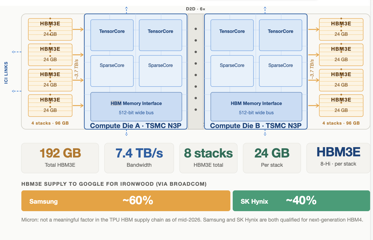 图09|原文配图(DataGravity)
Samsung holds approximately 60% of HBM3E supply to Google via Broadcom for Ironwood, with HBM4 already qualifying through Broadcom’s test process for the next generation. SK Hynix supplies the remaining ~40%. Micron is not a meaningful factor in this supply chain as of mid-2026.
Optical Interconnects — a differentiated layer
This is the layer most investors underestimate. Google’s Apollo OCS architecture is a full architectural break from conventional switching, and the qualified supplier base is narrow.
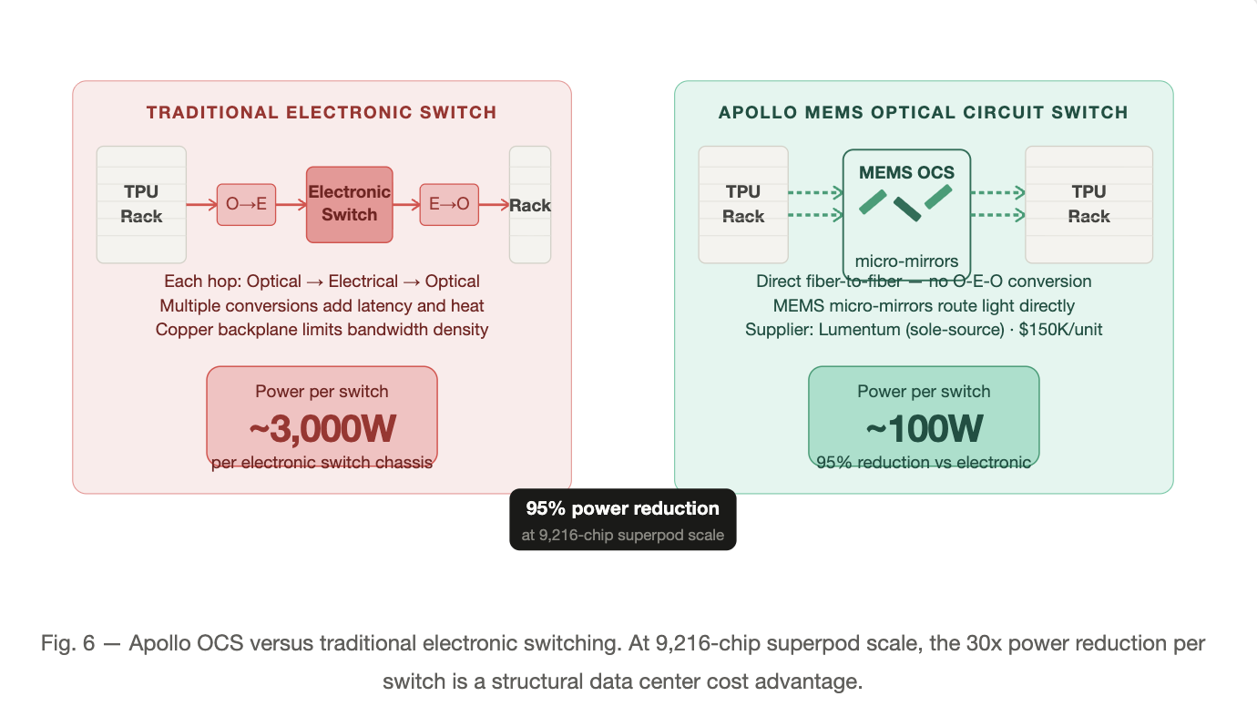 图10|原文配图(DataGravity)
Lumentum — Apollo OCS system
Lumentum supplies the MEMS-based optical circuit switches at the heart of Apollo. These switches use micro-mirrors to enable direct fiber-to-fiber connections, eliminating optical-electrical-optical conversions. A single Apollo switch draws ~100W versus ~3,000W for a comparable electronic switch — a 95% power reduction. Lumentum’s primary commercial product is a 300×300 OCS at approximately $150,000 per unit (~$500/port). In 2025, Google deployed an estimated 12,000–15,000 units. Lumentum is the sole-source supplier for this component; there is no qualified alternative in production.
Innolight and Eoptolink — 800G+ transceivers
Every cross-cabinet link in an Ironwood pod runs on 800G or 1.6T optical transceivers. TrendForce projects Innolight — the larger of the two and Google’s primary silicon photonics collaborator on 1.6T development — will capture ~80% of Google’s 800G+ optical module orders in 2026. Eoptolink captures most of the remainder; it is a second-tier supplier by volume but strategically important for supply chain resilience. The company posted 179% revenue growth in 2024, driven by cloud operator direct sales, and has built a manufacturing facility in Thailand specifically to serve North American demand outside Chinese export-control exposure. Collectively, Google’s Ironwood architecture is projected to push 800G+ transceiver share above 60% of all optical module demand by 2026 (TrendForce).
System Assembly — Server ODMs
TPU chips and optical components must be integrated into server platforms and racks. Taiwan-based ODMs dominate this work. Inventec is the most clearly confirmed primary ODM for Google’s TPU server builds, with management publicly expressing confidence in double-digit ASIC server shipment growth in 2026. Wiwynn (a Wistron subsidiary) is actively expanding SMT production capacity in Malaysia for ASIC server assembly. Quanta, Foxconn, and Mitac are all competing for additional allocation.
ASIC server shipments are forecast to grow 64.2% in 2026 versus 43.8% for GPU servers. The margin dynamic favors ODMs: ASIC servers carry lower unit prices than GPU platforms but require more customized design work and longer production runs, which compresses per-unit revenue while improving margin mix. The net effect is that ODM revenue from ASIC servers grows more slowly than volume, but profitability improves as ASIC share of the revenue mix increases.
Beneficiary Summary
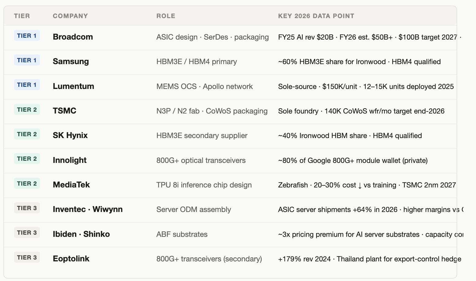 图11|原文配图(DataGravity)
Closing Thesis
The companies with clearest structural exposure are Broadcom (silicon implementation, locked through 2031), Samsung (HBM memory, primary qualified supplier), and Lumentum (optical switching, sole-source). These are not cyclical trades on AI capex — they are design partners with multi-year roadmaps and switching costs measured in years.
At $175–185B in committed 2026 capex and 3.3–4.6M projected TPU shipments, the question is no longer whether Google’s custom silicon program is real. The question worth stress-testing is what breaks the thesis. Three scenarios are worth watching: first, CoWoS yield issues at TSMC N2 that compress 2027 volumes below the 5M unit consensus — this directly impairs every vendor in the stack. Second, Samsung HBM4 qualification delays that concentrate more supply at SK Hynix and introduce a single-source risk Google has spent years trying to avoid. Third, Nvidia closing the inference cost-per-token gap faster than expected through Blackwell derivatives — this doesn’t threaten Broadcom’s training revenue, but it limits how aggressively Google can price TPU inference access externally, which is increasingly the commercial justification for the capex.
None of these scenarios break the supply chain. They delay it and compress near-term returns for the vendors most dependent on volume ramp. The structural position of the Tier 1 beneficiaries — design lock-in, sole-source components, multi-year agreements — survives all three. What changes is the timeline, not the destination.
Sources / Recommended readings: SemiAnalysis: Google TPUv7 — The 900lb Gorilla Google Cloud: Inside the Ironwood TPU codesigned AI stack The Next Web: Google assembles four-partner chip supply chain TrendForce: Global AI Server Shipments Forecast 2026 TrendForce: Google’s 800G+ Optical Transceiver Push KED Global: Samsung leads HBM for Google Ironwood (~60% share) DigiTimes: Google TPU stays strong, Inventec confident 2026 DigiTimes: Google TPU demand vs CoWoS and memory constraints Gazettabyte: Lumentum OCS for AI data centres Oplexa: Broadcom Google TPU Deal 2026 CNBC: Alphabet plans $80B equity raise Broadcom: FY2025 Annual Results Tom’s Hardware: Custom AI ASICs — state of play, May 2026
第二部分:解析(深度解读)
以下为基于原文的结构化中文解读,仅供学习交流,不代表原作者观点。
一、这篇文章在讲什么
DataGravity 这篇《Google’s TPU Supply Chain》拆解谷歌 TPU 从架构定义到量产的供应链骨架:自研 ASIC(TPU 芯片本身)、前道代工(TSMC 等)、HBM(SK hynix/三星/美光)、先进封装(CoWoS 类)、基板/PCB、光模块与网络、以及整机 ODM/云部署。文章把「算力」还原成一条横跨多家供应商、任何一环卡住都会拖累交付的长链。
二、关键概念拆解
- 自研 ASIC + 代工:TPU 由谷歌设计、TSMC 代工,节奏受先进节点产能与良率约束。
- HBM 是生死线:每代 TPU 带宽需求靠 HBM 堆高,HBM 供给(尤其 SK hynix)与 CoWoS 封装产能是 TPU 放量的硬瓶颈。
- 先进封装(CoWoS):2.5D 中介层产能长期紧张,是 AI 加速器交付的「卡脖子」环节。
- 网络与光模块:TPU pod 的纵向扩展依赖高速互连与光模块,供应链延伸到光器件。
- ODM / 云部署:从基板、散热、电源到整机与数据中心,交付是系统工程。
三、与本站其他文章的衔接
- AI 硬件 / 推理芯片:TPU 是云端自研 AI 芯片的范本,与本站 AI 硬件/推理芯片架构系列直接对应。
- HBM / 内存之战:本文的 HBM 瓶颈与 siliconatlas「下一代 AI 内存」七路径互补——TPU 侧是需求,内存侧是供给。
- 先进封装 / CPO:CoWoS 瓶颈与 CPO 路线同源;光模块/光互连是 TPU pod 扩展的物理底座。
四、趋势与投资映射
- 投资主线:AI 算力瓶颈从「芯片设计」转移到「制造与封装供应链」——TSMC 先进节点、HBM 三巨头、CoWoS 封装、基板与光模块任一环节都是 α 来源。
- 风险:供给端高度集中(HBM 与 CoWoS 双垄断),任何产能不可抗力都会放大交付风险;自研 ASIC 的代工与封装绑定也意味着地缘与产能双重暴露。