A Deep Dive of GeSi Electro-Absorption Modulators and Marvell/Celestial AI's OMIB for 200Gbps+ Interconnects — 中文解读
Silicon Co-Design 深潜 Marvell/Celestial AI 的 GeSi 电吸收调制器与 OMIB 光互连桥,面向 200Gbps+ 单波长互连。
来源:Silicon Co-Design — A Deep Dive of GeSi Electro-Absorption Modulators and Marvell/Celestial AI’s OMIB for 200Gbps+ Interconnects 原文链接:https://www.siliconcodesign.com/p/a-complete-deep-dive-of-marvell-gesi 原文发布日:2026-07-08 | 作者:Silicon Co-Design 说明:本文为英文原文全文转载,附中文结构化解读。原文以英文写就,未作翻译;解读部分为整理归纳,不代表原作者观点。
第一部分:正文(Original Article)
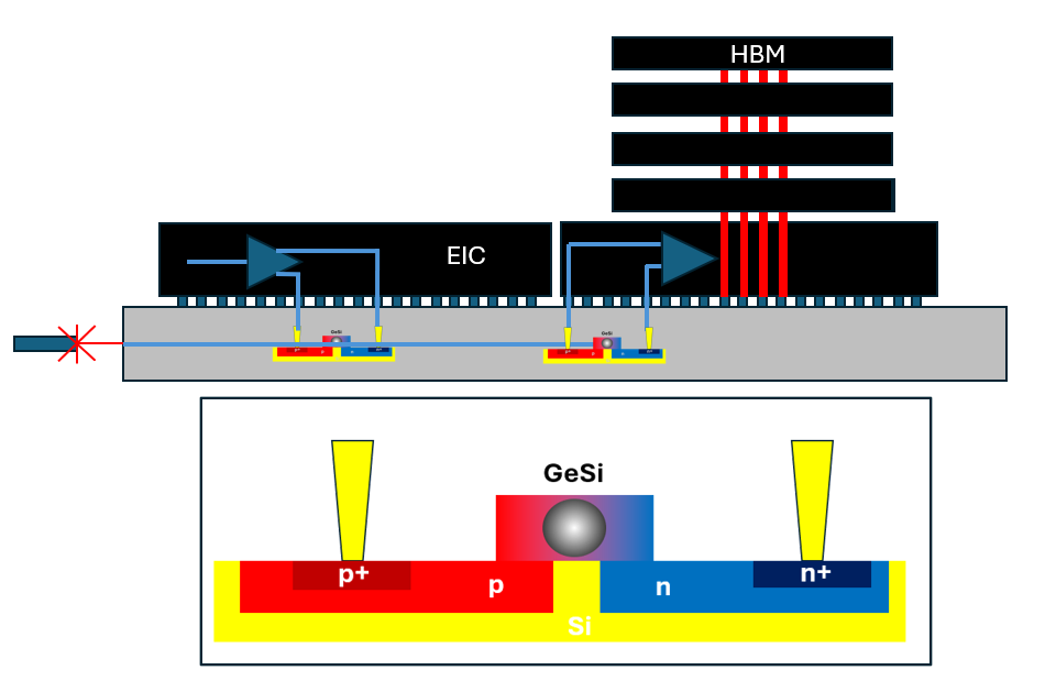 图01|原文配图(Silicon Co-Design)
I’ll be doing a deep dive into a few topics centered around Marvell/Celestial AI’s Electro-Absorption (EAM) approach to scaling optical interconnects. The outline of my post is as follows:
- Motivation behind Optical Interconnects
- An Overview of GeSi Electro-Absorption Modulator (EAM) Franz-Keldysh effect Comparison with other external modulation options
- 🔒Why Component Level Test Vehicles are Needed to Reduce Overall Integration Risk of 3D Heterogenous Integrated Packages
- 🔒An Introduction to Marvell’s Photonic Link: A Fully Integrated Solution for XPU, CPO, and HBM 🔒Marvell / Celestial OMIB: Overcoming Edge Density Constraints 🔒Photonic Fabric Test Vehicle of EIC, PIC, and FAU w/ measurement results 🔒Example 3D Packaged Application: Photonic Fabric Memory Module
- 🔒Key Co-design Integration Challenges 🔒Thermal Management 🔒EAM Thermal Stability 🔒Package Thermal Steady State Characteristics 🔒Package Thermal Transient Characteristics 🔒Power Delivery Challenges
- 🔒How NVIDIA DWDM and Marvell’s EAM technologies can be powerful together
Motivation behind Optical Interconnects
An Overview of GeSi Electro-Absorption Modulator (EAM)
- Franz-Keldysh effect
- Comparison with other external modulation options
Franz-Keldysh effect
Comparison with other external modulation options
🔒Why Component Level Test Vehicles are Needed to Reduce Overall Integration Risk of 3D Heterogenous Integrated Packages
🔒An Introduction to Marvell’s Photonic Link: A Fully Integrated Solution for XPU, CPO, and HBM
- 🔒Marvell / Celestial OMIB: Overcoming Edge Density Constraints
- 🔒Photonic Fabric Test Vehicle of EIC, PIC, and FAU w/ measurement results
- 🔒Example 3D Packaged Application: Photonic Fabric Memory Module
🔒Marvell / Celestial OMIB: Overcoming Edge Density Constraints
🔒Photonic Fabric Test Vehicle of EIC, PIC, and FAU w/ measurement results
🔒Example 3D Packaged Application: Photonic Fabric Memory Module
🔒Key Co-design Integration Challenges
- 🔒Thermal Management 🔒EAM Thermal Stability 🔒Package Thermal Steady State Characteristics 🔒Package Thermal Transient Characteristics
- 🔒Power Delivery Challenges
🔒Thermal Management
- 🔒EAM Thermal Stability
- 🔒Package Thermal Steady State Characteristics
- 🔒Package Thermal Transient Characteristics
🔒EAM Thermal Stability
🔒Package Thermal Steady State Characteristics
🔒Package Thermal Transient Characteristics
🔒Power Delivery Challenges
🔒How NVIDIA DWDM and Marvell’s EAM technologies can be powerful together
The research from this post comes from various Marvell’s papers from ECTC and their ISSCC forum presentation. I also incorporate relevant fundamental material from ISSCC short courses as well when developing the theory.
This post is aimed at more advanced understanding of some of the cross domain integration challenges that EAM is facing. Fortunately, I provide several references to several of my posts on advanced packaging, optical communications, and power architecture for all knowledge levels to understand the underlying fundamentals of Marvell’s Photonic Fabric Technology.
Before writing this, I wrote a similar deep dive on NVIDIA DWDM summarizing the challenges from both their ISSCC and ECTC papers, having attended both conferences myself. These posts come at a timely moment when NVIDIA recently announced they invested $2B into Marvell and Jensen announced at Computex that Marvell will be the next $1T company, causing the stock to soar.
I recommend you read my other NVIDIA post to put GeSi into its proper context and to read between the lines behind that stance:
Motivation behind Optical Interconnects
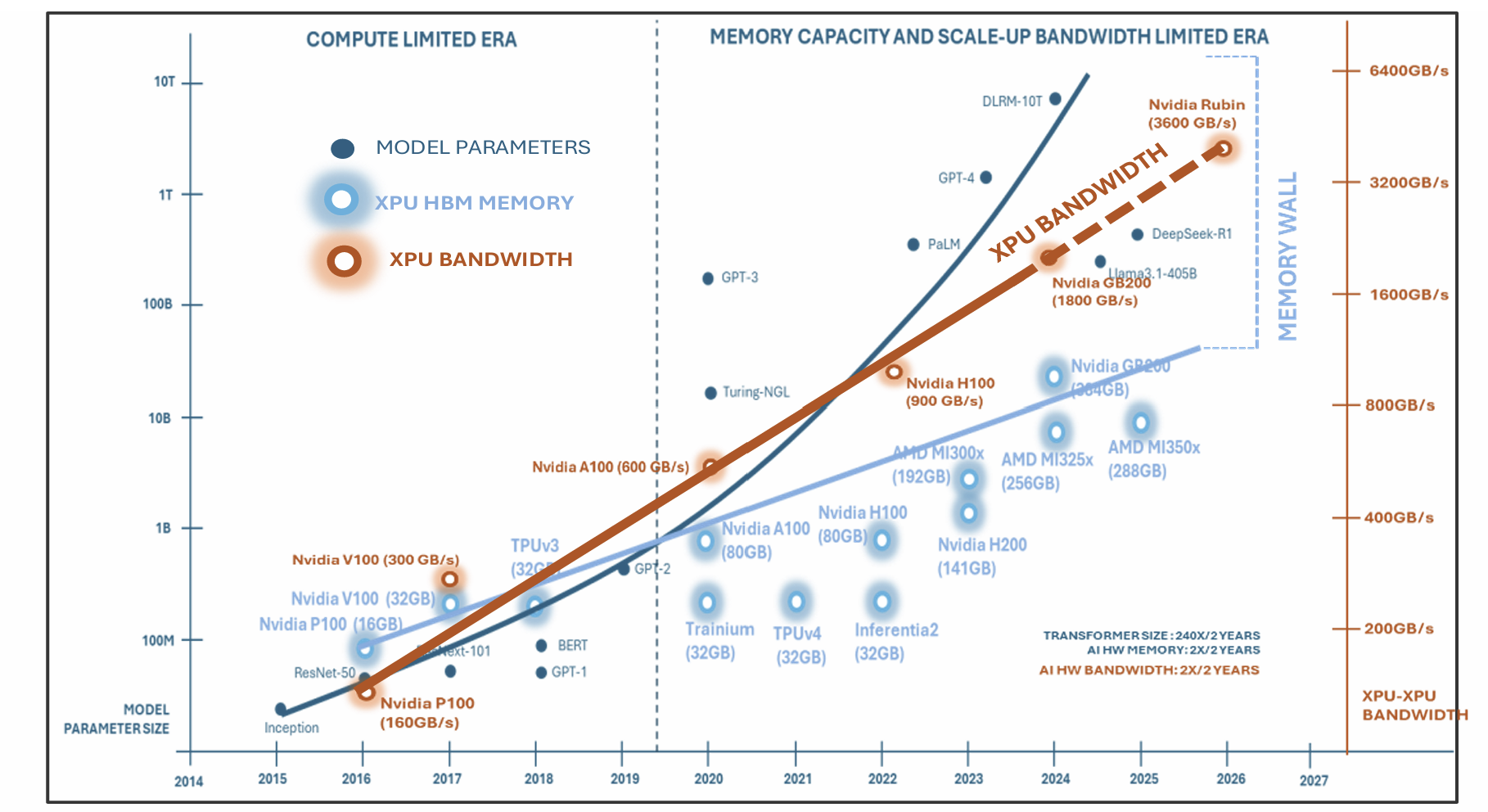 图02|原文配图(Silicon Co-Design)
Scaling AI compute has many different bottlenecks: power delivery, thermal, and high speed interconnect density. Industry standard interconnects such as PCIe have limitations for the workloads AI compute demands. As a result, there is demand for high bandwidth, long reach interconnects that makes optical communications such an attractive option.
Within the optical domain, lasers themselves can be directly modulated (such as VCSELs) or light coming from lasers can be externally modulated . There are three primarily ways to externally modulate a light in the optical domain: Mach-Zehnder Interferometers (MZI) , Ring , and Electro-Absorption . MZI modulates the phase of light travelling through two arms to cause destructive interference when recombined, and ring modulators act as band-stop filters for specific wavelengths of light.
I discuss these options in the following post:
GeSi Electro-Absorption modulators
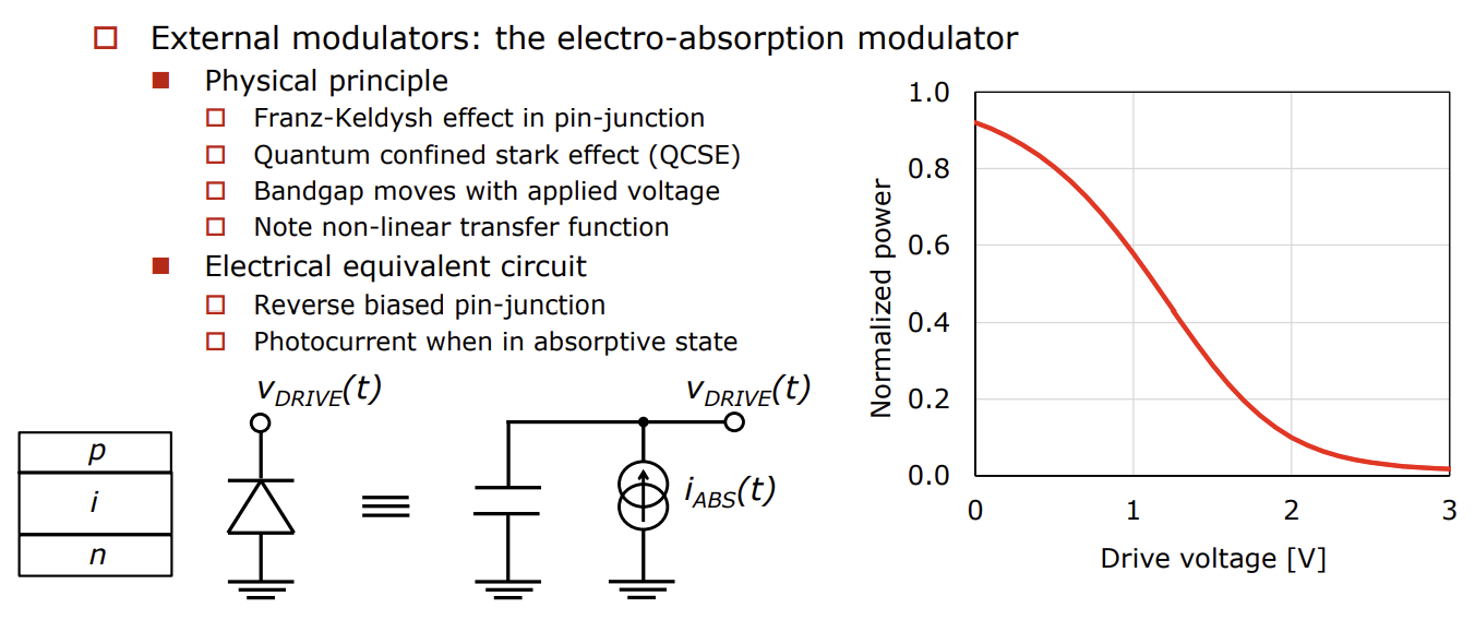 图03|原文配图(Silicon Co-Design)
EAMs operate by optical absorption of light through an electrically-controlled PIN junction at a single wavelength. A PIN Diode is a PN junction diode with an undoped intrinsic region to alter the PN diodes characteristics for the desired application, such as:
- High-frequency RF switches / attenuators (Si, GaAs, InP),
- High voltage tolerance by lowering the capacitance and thus increases breakdown voltage (GaN, SiC),
- Photodetectors by converting optical signals to electric current through generation of Electron-Hole pairs (InGaAs, Ge)
High-frequency RF switches / attenuators (Si, GaAs, InP),
High voltage tolerance by lowering the capacitance and thus increases breakdown voltage (GaN, SiC),
Photodetectors by converting optical signals to electric current through generation of Electron-Hole pairs (InGaAs, Ge)
In optical communications, EAMs device have a high bandwidth and a fairly compact footprint for CPO applications.
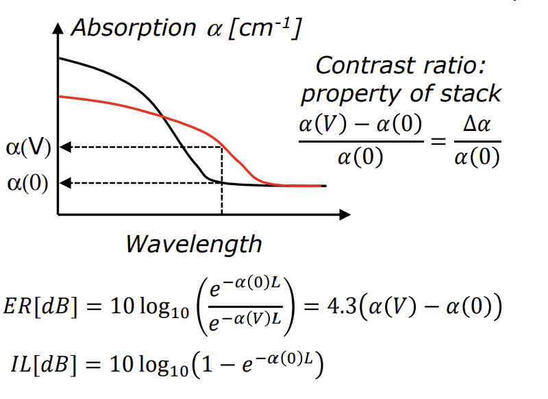 图04|原文配图(Silicon Co-Design)
EAMs have a property called the Franz-Keldysh effect which is where the optical absorption in a semiconductor changes when an electric field is applied. This is shown as the black curve above shifting to the red curve when a bias voltage is applied. This allows a fixed wavelength light to be externally modulated at high speeds by quickly switching the absorption curve at that wavelength to affect how much light goes through.
As shown in the equations above, the extinction ratio can be calculated as the ratio of the exponentials of the absorption factors of the two states, and the insertion loss can be calculated as the exponential of the absorption at 0V. Higher extinction ratio and lower insertion loss is desired.
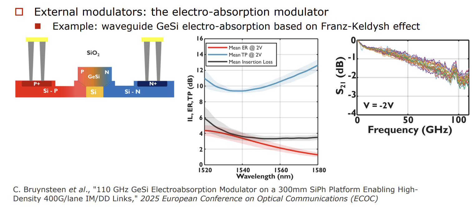 图05|原文配图(Silicon Co-Design)
GeSi is a common material used for the intrinsic region. The GeSi is epitaxially grown on top of a flat surface that is polished with CMP. Light is routed through the GeSi which has a higher refractive index than the surrounding SiO2, thus causing total internal reflection through the device.
One common FoM is the the transmitter penalty (TP) which is a measure of the loss due to the modulation itself and combines both the IL and ER:
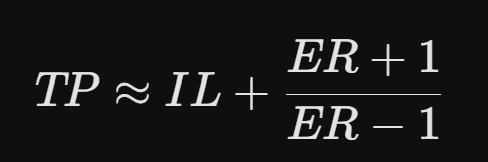 图06|原文配图(Silicon Co-Design)
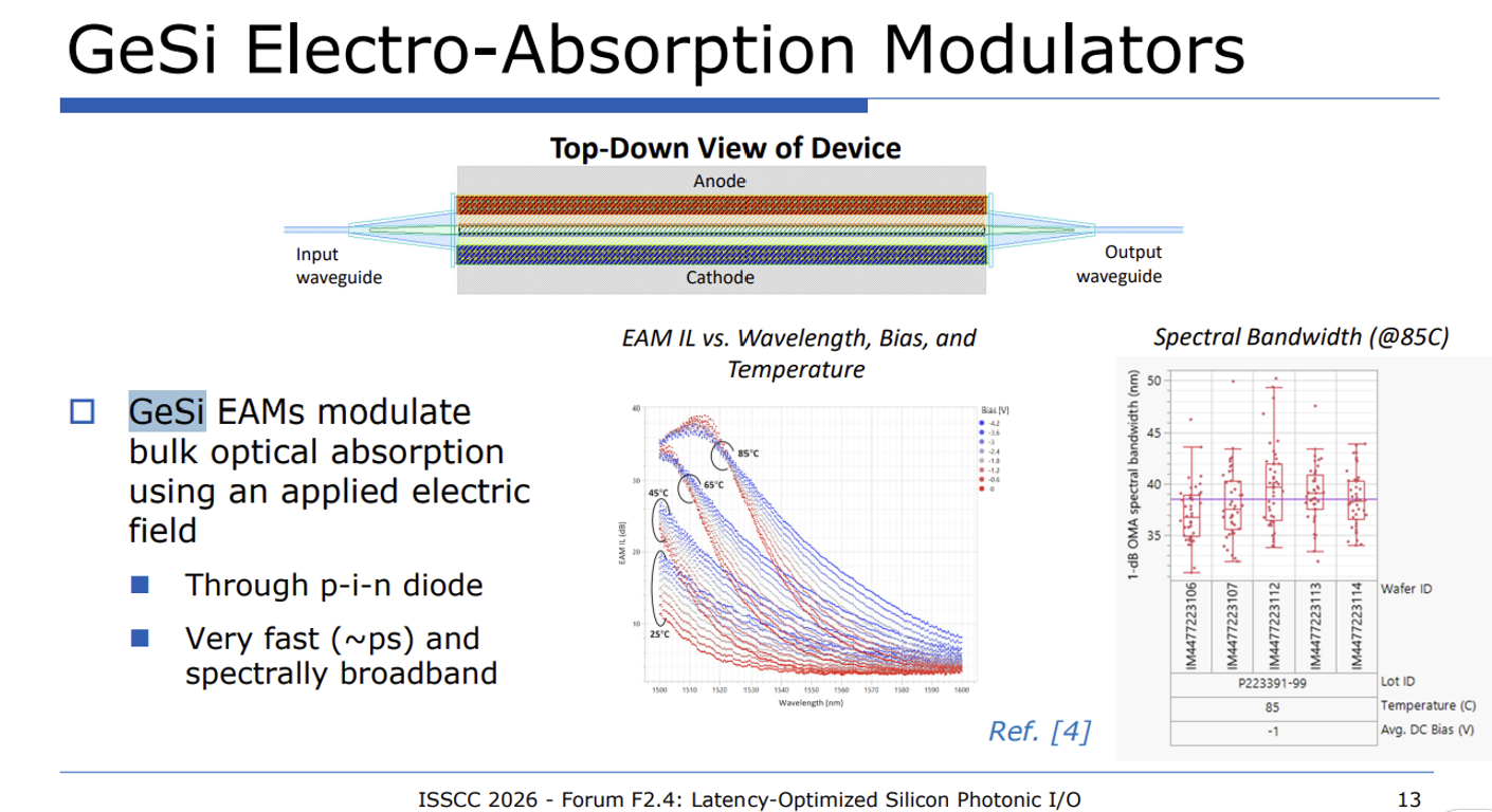 图07|原文配图(Silicon Co-Design)
Here we see some example characteristics of Marvell’s EAM IL over wavelength over bias voltage and different temperatures. High temperature causes the IL to shift up and affect the absorption that each signal level sees.
This means that temperature stability and thermal management is crucial to ensuring that EAM devices can operating consistently within its intended environment. Sophisticated mixed circuit control circuitry is necessary to anticipate and correct for rapid temperature swings in the GPU and package.
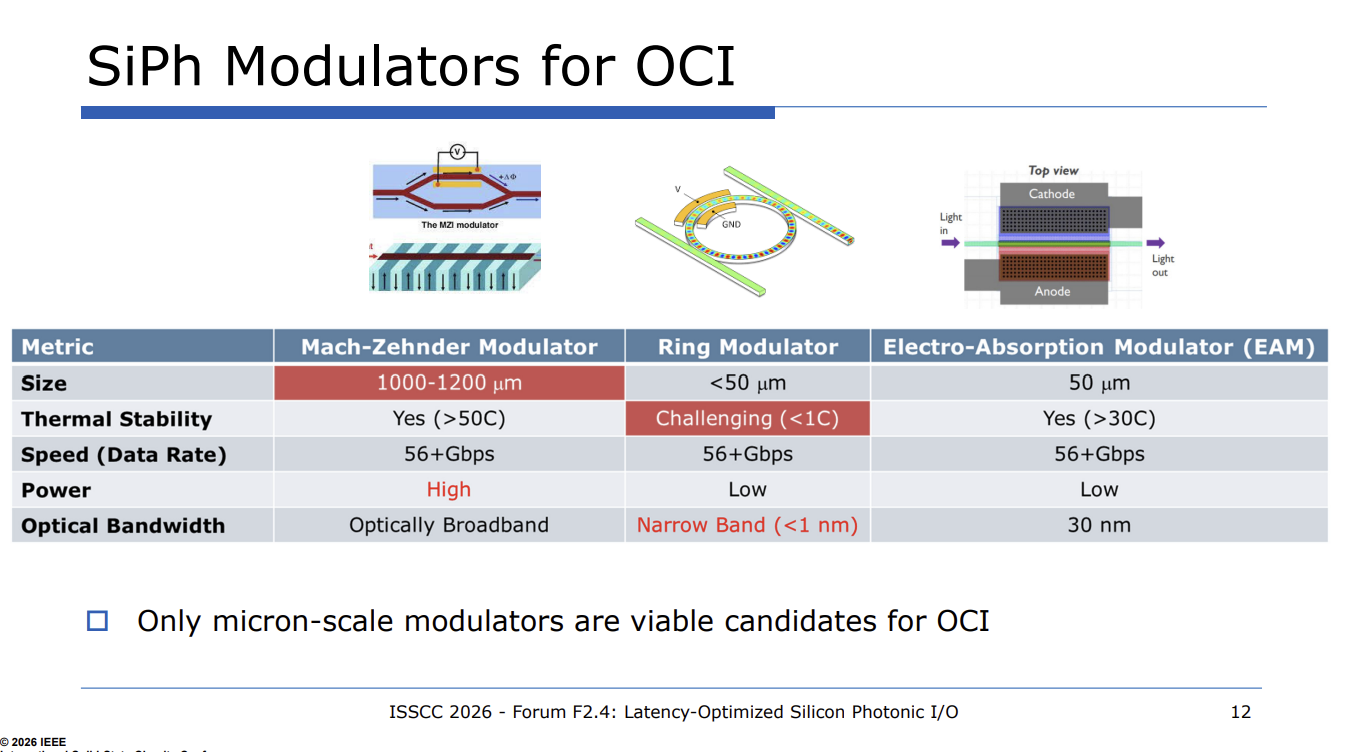 图08|原文配图(Silicon Co-Design)
While ring modulators face challenges with precise thermal control and MZI are quite large, EAMs offer a promising “middle range” alterative in high performance CPO applications. Advantages include:
- Relatively small size
- Good thermal stability
- High speed
- Low power
- High optical bandwidth
Relatively small size
Good thermal stability
High speed
Low power
High optical bandwidth
However, there are a few downsides:
- EAMs struggle from power handling because they absorb light, not phase shift it. There is an almost guaranteed 3dB loss from light passing through the EAM that must be accounted for in the link budget. I believe the link budget is an extremely important concept that anyone investing in or designing optics needs to know because it affects which components in the supply chain can be successfully integrated in real systems. I dive more into link budgets here in the free section:
- EAM devices are non-linear that, if uncorrected, affects the size of the individual eyes for PAM4 where the noise margin is governed by the smallest one. To combat this, pre-distortion circuits are needed to pre-distort the four voltage levels so that the signal can be sent through the channel and recovered as linearly as possible.
- EAM devices are difficult to reliably manufacture at scale. Growing the GeSi epitaxially requires a fairly flat surface and sophisticated means to control the crystal growth. High volume testing is needed to screen for KGD.
EAMs struggle from power handling because they absorb light, not phase shift it. There is an almost guaranteed 3dB loss from light passing through the EAM that must be accounted for in the link budget.
- I believe the link budget is an extremely important concept that anyone investing in or designing optics needs to know because it affects which components in the supply chain can be successfully integrated in real systems. I dive more into link budgets here in the free section:
I believe the link budget is an extremely important concept that anyone investing in or designing optics needs to know because it affects which components in the supply chain can be successfully integrated in real systems. I dive more into link budgets here in the free section:
EAM devices are non-linear that, if uncorrected, affects the size of the individual eyes for PAM4 where the noise margin is governed by the smallest one.
- To combat this, pre-distortion circuits are needed to pre-distort the four voltage levels so that the signal can be sent through the channel and recovered as linearly as possible.
To combat this, pre-distortion circuits are needed to pre-distort the four voltage levels so that the signal can be sent through the channel and recovered as linearly as possible.
EAM devices are difficult to reliably manufacture at scale. Growing the GeSi epitaxially requires a fairly flat surface and sophisticated means to control the crystal growth. High volume testing is needed to screen for KGD.
In short, GeSi offers several promising benefits for CPO, but does suffer from inherent device level challenges as well as circuit complexity challenges to control the characteristics of the PAM4 signal.
Why Component Level Test Vehicles are Needed to Reduce Overall Integration Risk of 3D Heterogenous Integrated Packages
There are several excellent research works being performed across the industry and academia on components that comprise integrated 3D packaging solutions:
- Different substrates : organic, silicon, glass
- Different bridge option : LSI, embedded bridge
- Interconnect options : C2, C4, and Hybrid bonding
- Different integration options : 2.1D, 2.3D, 2.5D 3D, 3.3D, 3.5D.
- Different optical component integration and waveguide routing options in each substrate
Different substrates : organic, silicon, glass
Different bridge option : LSI, embedded bridge
Interconnect options : C2, C4, and Hybrid bonding
Different integration options : 2.1D, 2.3D, 2.5D 3D, 3.3D, 3.5D.
Different optical component integration and waveguide routing options in each substrate
Here are several of my other posts that give you a fundamental understanding of the key tradeoffs in each of these areas:
第二部分:解析(深度解读)
以下为基于原文的结构化中文解读,仅供学习交流,不代表原作者观点。
一、这篇文章在讲什么
Silicon Co-Design 这篇深潜讲 Marvell 与 Celestial AI 的 GeSi(锗硅)电吸收调制器(EAM)与 OMIB(光互连桥)方案,面向 200Gbps+ 单波长互连。文章把「用 GeSi 做调制器」放回硅光平台的工程语境:如何在成熟 CMOS 工艺上集成低功耗、高带宽的电吸收调制,并以 OMIB 这类桥接结构把光引擎与计算/交换芯片共封装。
二、关键概念拆解
- GeSi EAM(电吸收调制器):在锗硅上实现电吸收调制,相比 Mach-Zehnder 更紧凑、更低电容,适合 200G+/波长的高速直调。
- 为什么是 GeSi:与硅光工艺兼容、可在同一 CMOS 线集成,潜在成本与良率优势;挑战在 Ge 应变、暗电流与带宽-损耗折中。
- OMIB(Optical Interconnect Bridge):把光引擎/光子层以桥接方式贴近主机芯片,缩短电走线、提升带宽密度与能效——是 CPO 的一种实现形态。
- 200Gbps+ 单波长:单波长速率提升直接摊薄光器件与封装成本,是线性/CPO 光链路的经济临界点。
- 与 CPO 的关系:OMIB 是「光引擎就近」思路的工程落地,呼应本站 CPO 系列「把 TRx 封进封装、剩余走光」的主线。
三、与本站其他文章的衔接
- CPO / 光互联系列:GeSi EAM + OMIB 是 CPO 在「调制器材料 + 桥接封装」层面的具体技术选项,与 SK hynix 路线图、PhotonCap、Intel 微环 DWDM 等互补。
- 先进封装:OMIB 本质是 2.5D/桥接式先进封装的光学延伸。
- SerDes / 速率:200G+ 单波长直接对标电 SerDes 的 224/448G 替代路径。
四、趋势与投资映射
- 投资主线:CPO 落地的「材料-器件-封装」三重卡点——GeSi/硅光调制器、低功耗光引擎、桥接/共封装结构;Marvell、Celestial AI 及硅光代工/器件厂是观察标的。
- 风险:GeSi EAM 的带宽-损耗-良率三角仍待量产验证;OMIB 类方案与 Intel 微环、其它 CPO 形态存在路线竞争,标准与生态未定。