Design for Testability (DFT): How Do We Know a Chip Actually Works? — 中文解读
入门科普:芯片流片后如何测出制造缺陷——从扫描链、ATPG 到 MBIST、OCC、测试压缩与 IJTAG。
来源:Chip-chat with Shyam — Design for Testability (DFT): How Do We Know a Chip Actually Works? 原文链接:https://heyitshyam.substack.com/p/design-for-testability-dft-how-do 原文发布日:2026-08-13 | 作者:Shyam(heyitshyam) 说明:本文为英文原文全文转载,附中文结构化解读。原文以英文写就,未作翻译;解读部分为整理归纳,不代表原作者观点。
第一部分:正文(Original Article)
Designing a semiconductor chip is not only about making it perform its intended function.
A chip may work perfectly in simulation, yet once it is manufactured, physical defects can occur during fabrication. These defects can cause a chip to fail even though the RTL design itself is correct.
So, an important question arises:
How do we test a manufactured chip and identify whether it has defects?
This is where Design for Testability (DFT) comes in.
What is DFT?
Design for Testability is a set of design techniques used to make an integrated circuit easier to test after manufacturing.
The basic idea is simple:
Design the chip in a way that allows us to control and observe its internal logic during testing.
Without DFT, many internal nodes and flip-flops of a complex chip would be difficult or even impossible to access directly from the external pins.
DFT adds structures that improve:
- Controllability — ability to control internal circuit nodes
- Observability — ability to observe internal circuit behavior
- Fault detection — ability to identify manufacturing defects
Where Does DFT Fit in the ASIC Flow?
DFT is not something that happens only at the end of chip development. Test structures need to be considered as part of the overall ASIC design flow.
A simplified flow looks like:
Specification → RTL Design → Synthesis → DFT Insertion → Floorplanning → Placement → CTS → Routing → Verification → GDSII
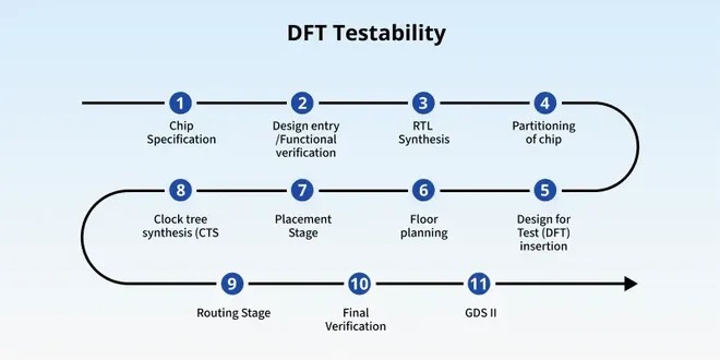 图01|原文配图(Chip-chat with Shyam)
During DFT insertion, additional test logic and structures are introduced into the design.
The final physical implementation must also consider these structures because scan chains, test logic, clocks, routing, timing, and area are all interconnected.
The Foundation: Scan Chains
One of the most fundamental DFT techniques is scan design.
In a normal functional design, flip-flops store the state of the circuit during operation. During testing, these flip-flops can be converted into scan flip-flops and connected together to form a scan chain.
Conceptually:
Scan In → FF → FF → FF → FF → Scan Out
During shift mode, test data can be shifted into the chain.
During capture mode, the circuit’s response to a test pattern is captured by the scan flip-flops.
The captured data can then be shifted out and compared with the expected response.
This gives testers a way to access and observe internal sequential logic.
What About ATPG?
Once scan structures are available, we need test patterns that can detect possible manufacturing faults.
This is where ATPG — Automatic Test Pattern Generation comes in.
ATPG tools generate patterns designed to detect fault models such as:
- Stuck-at faults
- Transition faults
- Bridging faults
- Other defect-related fault models
For example, a stuck-at fault assumes that a signal is permanently stuck at logic 0 or 1.
The ATPG tool attempts to generate an input pattern that activates the fault and propagates its effect to an observable point, such as a scan output.
DFT Goes Beyond Scan and ATPG
Scan and ATPG are only part of the larger DFT landscape.
As chips become more complex, different types of memories, clock domains, power domains, and embedded IPs require specialized test techniques.
Some important areas include:
MBIST — Memory Built-In Self-Test
Modern SoCs can contain a large number of embedded memories.
Testing these memories using only external test equipment can be difficult and expensive.
MBIST adds dedicated logic that can test embedded memories using predefined memory test algorithms.
It can detect memory-specific faults such as:
- Stuck-at faults
- Transition faults
- Address decoder faults
- Coupling faults
- Read/write related faults
OCC — On-Chip Clock Controller
Testing designs with multiple clock domains introduces additional challenges.
On-chip clock control structures help generate and control test clocks during scan and at-speed testing while maintaining the required timing relationships.
Test Compression
Large designs can contain millions of scan elements.
Shifting all test data directly through external pins can result in enormous test time and test data volume.
Test compression techniques reduce this overhead by compressing and decompressing test data.
IJTAG
As SoCs integrate more embedded instruments and test structures, accessing those instruments becomes increasingly important.
IEEE 1687 (IJTAG) provides a standardized methodology for accessing embedded instruments within an integrated circuit.
Why Is DFT Important?
A semiconductor manufacturing process can introduce defects that are not visible during normal functional simulation.
DFT provides a systematic way to test manufactured chips and improve defect detection.
It ultimately helps answer a critical question:
Did the manufactured silicon implement the intended design correctly?
The goal is not simply to make a chip functional.
The goal is to make the chip testable, diagnosable, and manufacturable at scale.
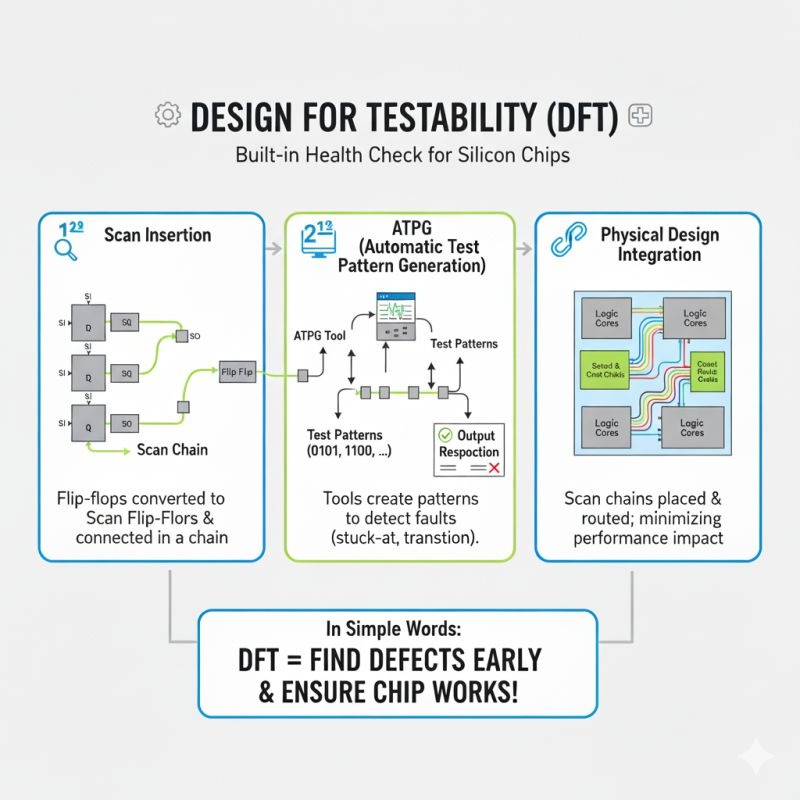 图02|原文配图(Chip-chat with Shyam)
What I’ll Be Exploring Here
This is the beginning of my journey into writing about VLSI and semiconductor engineering.
In upcoming posts, I’ll explore topics across:
DFT & ATPG
Scan chains, fault models, test compression, OCC, test points, IJTAG and more.
MBIST & Memory Testing
Memory architectures, fault models, MBIST controllers, test algorithms and practical implementation concepts.
RTL Design & Design Verification
Verilog/SystemVerilog, RTL design, simulation, assertions, UVM, CDC, formal verification and related concepts.
Semiconductor Industry Updates
A weekly roundup of important semiconductor news, technologies, companies, manufacturing developments and industry trends — explained from an engineering perspective.
My goal is simple:
«Learn. Build. Share.»
If you’re also interested in VLSI, DFT, MBIST, Design Verification, or the semiconductor industry, follow along. There is a lot to explore.
第二部分:解析(深度解读)
以下为基于原文的结构化中文解读,仅供学习交流,不代表原作者观点。
一、这篇文章在讲什么
Chip-chat with Shyam 的这篇入门科普讲清楚一个根本问题:芯片在仿真里是对的,流片后却可能因制造缺陷失效——怎么测出它到底有没有缺陷?答案就是 DFT(可测试性设计)。文章从 ASIC 流程切入,说明 DFT 不是最后补一刀,而是贯穿规格→RTL→综合→DFT 插入→布局→CTS→布线→验证→GDSII 的整体考量,并依次展开扫描链、ATPG、MBIST、OCC、测试压缩、IJTAG 等核心模块。
二、关键概念拆解
- DFT 三要素:可控性(control)、可观测性(observe)、故障检测(fault detection)——让内部节点与触发器能从外部引脚访问。
- 扫描链(Scan Chain):把功能触发器改成扫描触发器串成链,shift 模式灌入测试向量、capture 模式抓响应、再 shift 出来比对,从而观测时序逻辑。
- ATPG(自动测试向量生成):针对 stuck-at、transition、bridging 等故障模型生成能「激活并传播故障」到可观测点的向量。
- MBIST:片上专用逻辑用预设算法测嵌入式内存(stuck-at/transition/地址译码/耦合/读写故障)。
- OCC / 测试压缩 / IJTAG:多时钟域的片上时钟控制、海量扫描数据的压缩解压、IEEE 1687 标准化访问片上仪器。
三、与本站其他文章的衔接
- 先进封装 / 多 die:chiplet 时代裸片数量与类型暴涨,DFT/MBIST/IJTAG 是「裸片已知良率 + 系统级测试」的前提,与本站先进封装系列同频。
- AI 硬件 / 制造:大模型芯片面积与复杂度飙升,测试成本与良率直接决定 BOM 与毛利,是 AI 硬件量产的暗线。
- 半导体工艺(GAA/CFET):新工艺节点变异增大,DFT 与良率工程的权重同步上升。
四、趋势与投资映射
- DFT/ATPG/MBIST 是半导体「制造闭环」的刚需,EDA 测试签核(Synopsys/TetraMax、Siemens 等)与测试设备(ATE)长期稳健。
- 趋势:chiplet、3D 堆叠、多时钟/多电源域让测试从「单芯片」走向「系统级测试访问」,IJTAG/测试压缩价值提升。
- 风险:测试 IP 与 EDA 高度绑定大厂生态,新进入者门槛高;但 AI 与先进封装带来的测试复杂度上升是确定性增量。