CPO's Biggest Bottleneck Is Not Optics—It Is High-Volume Testing — CPO 的最大瓶颈不是光学,是量产测试
TSPA Semiconductor 深度分析:当 CPO 从实验室走向量产,真正的瓶颈不是光子芯片设计、不是封装,而是能否建立可重复、自动化、标准化、经济可行的光电混合测试体系。Advantest 在 SEMICON Taiwan 2025 的演讲指出了硅光/CPO 量产测试的四大关键方向与三大缺口。英文原文 + 中文深度解读。
本文整理自 TSPA Semiconductor (Substack) 的深度分析,原文发布于 2026-07-27(标题原文:CPO’s Biggest Bottleneck Is Not Optics—It Is High-Volume Testing)。 结构为 正文(英文原文)+ 解析(中文深度解读),方便中英对照阅读。 来源说明:内容经 Substack 公开页面获取,全文可读;本发布保留完整英文原文并附中文深度解读,仅作信息整理与学习用途,著作权归原作者所有,建议在 Substack 支持原作者订阅。
第一部分:正文(Original Article)
CPO’s Biggest Bottleneck Is Not Optics—It Is High-Volume Testing
TSPA Semiconductor · Jul 27, 2026

Artificial intelligence (AI), high-performance computing (HPC), and hyperscale cloud environments are driving data volumes to unprecedented levels. As GPU clusters and distributed inference engines multiply, the limitations of today’s 224 Gbps infrastructure are clear. The next milestone—448 Gbps per lane—will reshape how data centers are built, cooled, and interconnected. This evolution is about more than speed. It’s about density, power efficiency, and scalability across the entire signal chain.
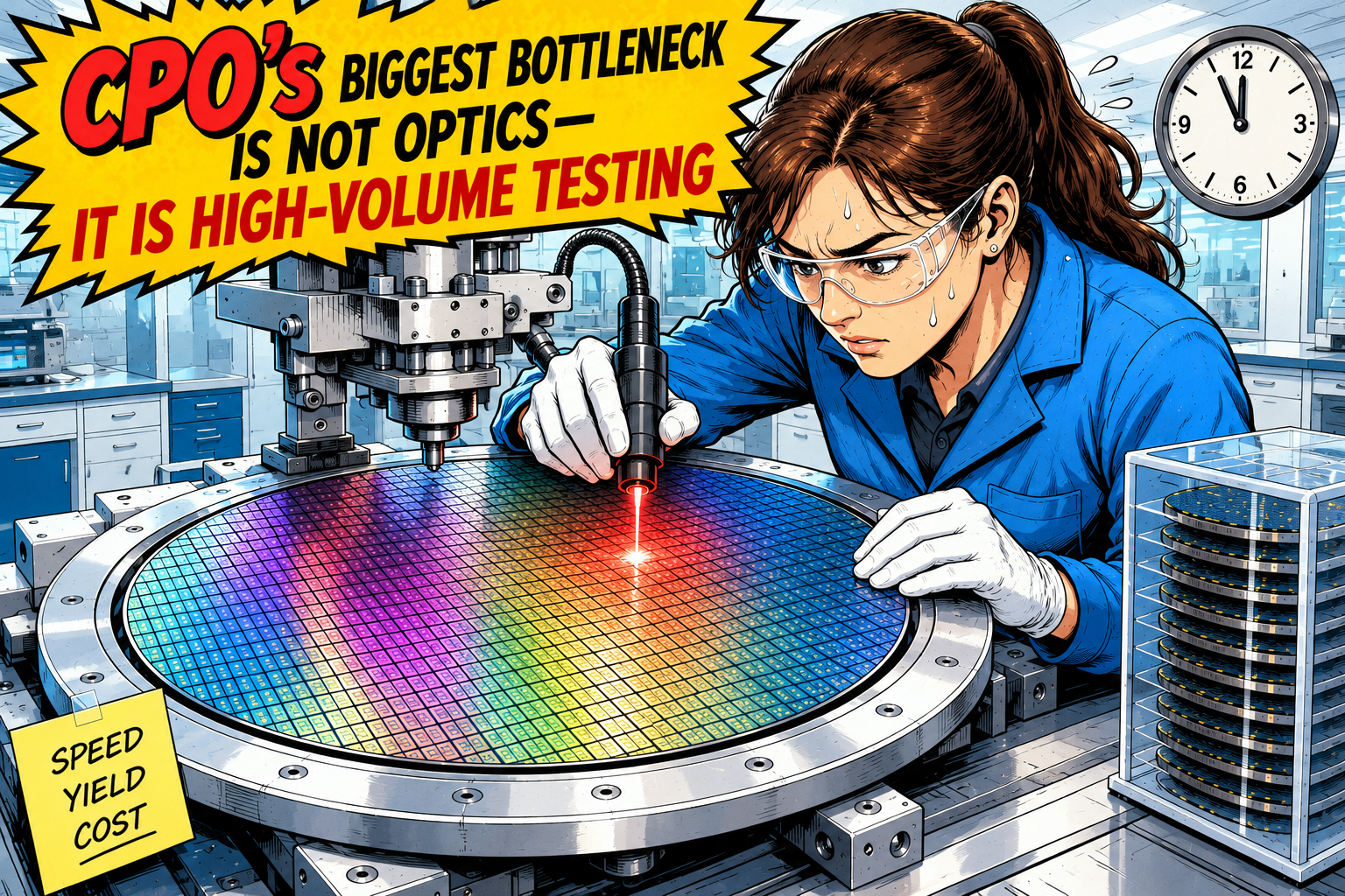
AI infrastructure is entering a new inflection point.
Over the past few years, the industry’s attention has been concentrated on GPUs, HBM, advanced packaging, CoWoS capacity, data center power delivery, and thermal architecture. However, as AI clusters expand from single-rack systems to multi-rack architectures, and from scale-out networking toward scale-up xPU fabrics, the real constraint on system efficiency is gradually shifting from “compute itself” to “how data moves within the system.”
In other words, the competitive focus of AI systems is moving away from the performance of a single chip and toward high-speed interconnect capability between chips, inside packages, and across racks.
This is why silicon photonics and co-packaged optics are moving from research topics into core issues for high-volume manufacturing. In its presentation at the SEMICON Taiwan SiPh Global Summit 2025, Advantest directly pointed out that SiPh/CPO has become a key enabling technology for future AI factories. Today, it is mainly applied in scale-out networking; the next stage will be scale-up xPU fabrics. In other words, optics will no longer be merely part of networking modules. It will move increasingly closer to ASICs, XPUs, and advanced packaging itself.
But this shift also brings a new challenge: once optics enters the package, testing can no longer follow the traditional logic of optical module production lines. Whether CPO can truly achieve mass production will not depend only on whether photonic chips can be designed, nor only on whether packaging can be completed. It will depend on whether the entire industry can establish a repeatable, automated, standardized, and economically viable electro-optical hybrid test system.
The evolution of AI servers is changing the position of the optical communications industry.
In traditional data center architectures, optical modules are mostly located outside the switch or rack, serving the role of long-distance, high-bandwidth data transmission. Optical modules have historically been peripheral I/O components of the system, with relatively clear boundaries separating them from ASICs, GPUs, HBM, and package substrates.
However, the development of AI data centers is breaking down this boundary. As the bandwidth requirements of GPUs, AI ASICs, HBM, and switch chips continue to rise rapidly, the key question is no longer simply whether the chip is fast enough. It is whether data can move in and out of the chip in real time.
The logic behind this shift is clear. Under high-speed, long-distance, and high-density conditions, copper interconnects face multiple challenges, including power consumption, signal integrity, thermal management, and package area constraints. As 800G, 1.6T, and even higher-speed standards become baseline requirements for AI data centers, relying solely on pluggable optical modules or traditional board-level interconnects is becoming increasingly insufficient for next-generation AI fabrics.
Therefore, the value of SiPh and CPO is not merely about converting electrical signals into optical signals. It is about redefining how data moves within computing systems.
In the past, optics mainly solved external system-level transmission problems. In the future, optics will increasingly address internal system interconnect problems. This means the battlefield for optical interconnects will gradually move from outside the rack, switch front panels, and optical module cages toward ASIC packages, interposers, substrates, and even chiplet interfaces.
This shift will have a profound impact on the semiconductor industry. Once optics enters the package, optical components are no longer independent and replaceable modules. Instead, they become part of the AI accelerator or switch chip itself. Future AI chip competition will not only be determined by logic process nodes, the number of HBM stacks, package size, or power delivery architecture. It will also depend on electro-optical conversion efficiency, optical I/O density, in-package optical routing design, fiber coupling stability, and test and yield management capability.
In other words, CPO is not simply an upgrade of optical communications. It is a reconstruction of AI system architecture.
Industry discussions around silicon photonics and co-packaged optics have traditionally focused on light sources, modulators, photodetectors, waveguides, packaging and coupling, laser integration, and system architecture. From a manufacturing perspective, however, the factor that will ultimately determine whether these technologies can enter the mainstream AI supply chain is the ability to establish a testing process that is scalable, automated, standardized, and economically viable.
Source: Advantest
This is one of the most underestimated challenges in the industrialization of CPO.
Building a functional optoelectronic device in a laboratory is fundamentally different from reliably testing hundreds of thousands—or even millions—of hybrid photonic-electronic devices on a production line. The former demonstrates technological feasibility; the latter demonstrates industrial capability. Laboratory validation can rely on engineers to tune equipment, perform calibration, and manually align optical interfaces. High-volume manufacturing, by contrast, requires automated equipment, standardized interfaces, stable calibration models, and high-throughput workflows.
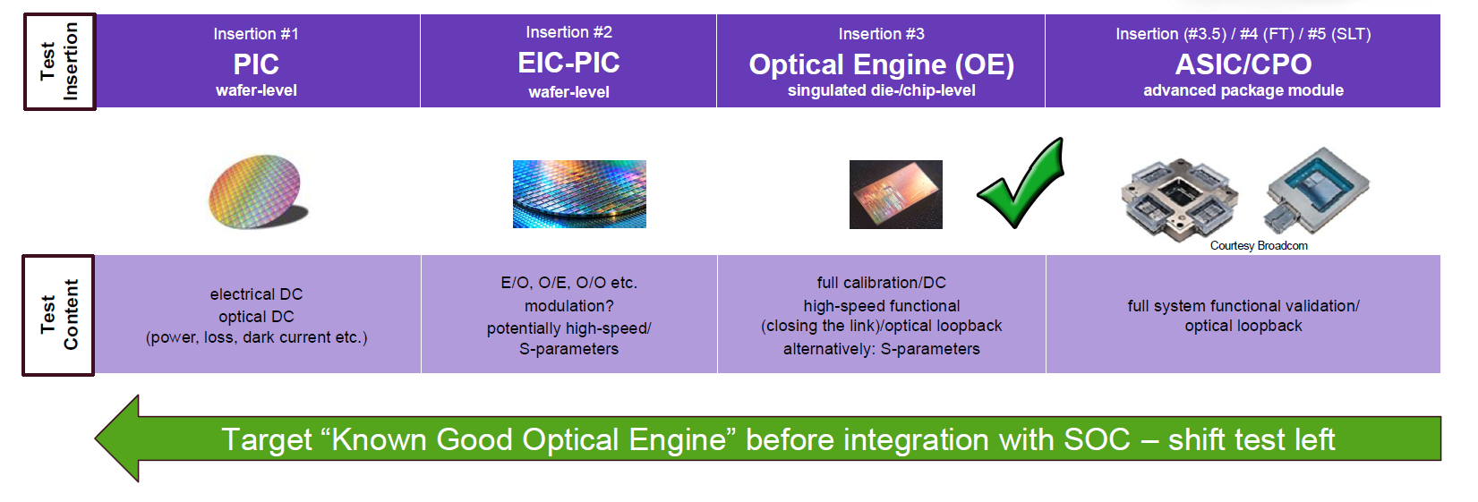
Advantest’s presentation divides the HVM test insertion points for PICs, optoelectronic devices, and CPO into several stages. The first is wafer-level testing of the photonic integrated circuit. The second is wafer-level testing of the integrated EIC-PIC structure. The third is testing of the optical engine at the singulated-die or chip level. Only after these stages does the process move to final testing or system-level testing of the advanced ASIC/CPO package.
The central objective is to establish a Known Good Optical Engine before the optical engine is integrated with the SoC. In other words, testing must be shifted left so that defective optoelectronic components can be identified before expensive packaging and system integration take place.
This is critically important for the AI semiconductor supply chain.
CPO and silicon photonics are not single-device technologies. They are highly integrated systems combining optical, electrical, thermal, mechanical, packaging, and software-control functions. Without visibility into yield at the wafer level or optical-engine level, the cost of downstream packaging failures can increase dramatically. In advanced packaging architectures such as CoWoS, EMIB, 3D ICs, and more complex xPU modules, the failure of a single optical engine could result in the loss of an entire high-value package.
This differs from the logic of conventional electrical IC testing. Traditional semiconductors can be screened progressively through wafer sort, final test, burn-in, and system-level test. In CPO, however, once optical components are integrated into the package, many defects may not be fully detectable through conventional electrical testing alone.
Optical-path loss, coupling efficiency, polarization sensitivity, temperature drift, laser stability, and fiber-alignment errors can all affect final system performance.
CPO mass production therefore requires more than simply adding another test station. It requires a fundamental redesign of the entire test insertion strategy.
In the era of advanced packaging, the concept of the Known Good Die has already become essential. In the CPO era, the industry will need to extend this principle to the Known Good Optical Engine.
The reason is straightforward: the more complex the package, the higher the cost of discovering failures at a later stage.
An AI accelerator package may integrate logic dies, HBM, an interposer, a substrate, a power-delivery network, a thermal solution, and optical engines. Each subsystem affects the final package yield. If an optical engine enters the packaging process without sufficient testing, defects such as excessive optical-path loss, unstable modulation performance, elevated photodetector dark current, or optical-loopback failure may only be discovered downstream, when opportunities for rework are already extremely limited.
This is why Advantest’s presentation places particular emphasis on shifting test left. The earlier a defect is identified, the lower the associated cost. The later it is discovered, the greater the financial impact.
For future AI systems, this will create a new question regarding the division of responsibilities across the supply chain: who is responsible for guaranteeing the quality of the optical engine? Is it the silicon-photonics foundry, the OSAT provider, the optical-engine vendor, the CPO switch supplier, or the hyperscaler defining and operating its own qualification framework?
This is not merely an engineering issue. It is also a commercial one.
Without common industry testing standards, each system customer may require different test items, calibration methodologies, yield definitions, and reliability conditions. This would directly increase supply-chain complexity and slow the commercialization of silicon photonics and CPO.
The future of CPO competition will therefore not be defined solely by component specifications. It will also be shaped by control over testing standards and by how responsibility for yield and quality is allocated across the supply chain.
The challenge facing high-volume SiPh/CPO testing today is not a complete lack of available tools, but rather the absence of a mature and standardized ecosystem.
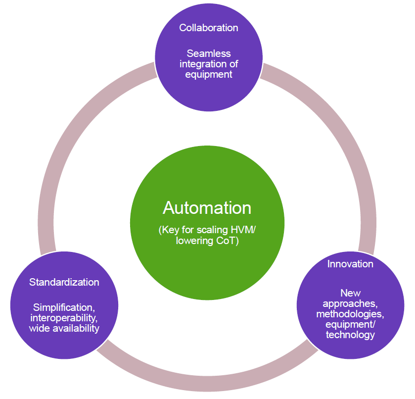
Advantest identified three major gaps.
First, there is still no true standard for optical probing. Current solutions continue to rely heavily on active multi-axis alignment, although passive alignment approaches are being explored.
Second, optical package fiber-connector handling remains largely unstandardized, with many processes still requiring manual intervention.
Third, optical instrumentation continues to depend heavily on rack-and-stack architectures, customized configurations, and complex optical-path calibration.
Source: Advantest
The fundamental issue is that optical testing has not yet fully adopted the operating model of semiconductor high-volume manufacturing.
Conventional IC testing emphasizes multisite testing, standardized fixtures, automated device handling, rapid calibration, and high throughput. Optical testing, however, introduces an additional layer of complexity: fibers, fiber-array units, waveguide facets, coupling efficiency, and optical-path loss can all affect measurement results.
Source: Advantest
In other words, the measured result may reflect not only the performance of the device under test, but also alignment accuracy, connector conditions, fiber-path loss, temperature drift, and calibration error.
This is one of the most difficult aspects of optical testing: the measurement system itself can easily become a significant source of error.
At the wafer-level probing stage, for example, electrical contact between the probe and the pad can be standardized relatively easily. Aligning an optical fiber with a grating coupler or edge coupler, however, requires precise control of three-dimensional positioning, angle, distance, polarization, and temperature.
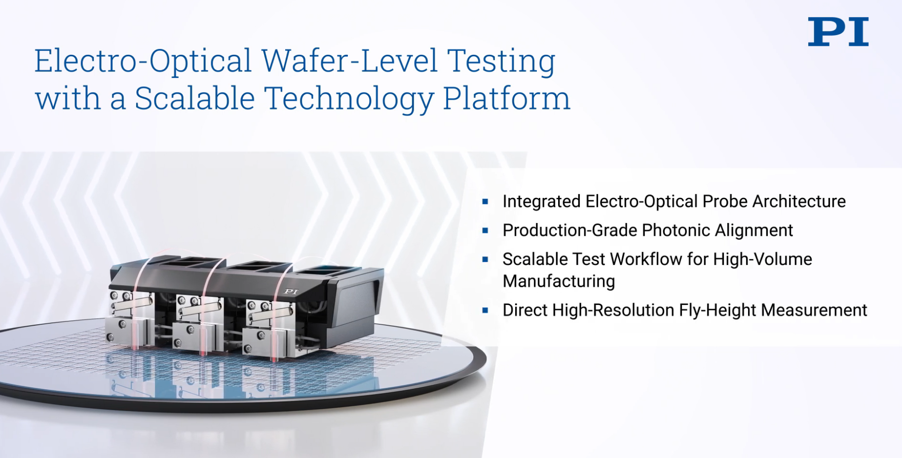
PI: Photonic wafer probing technology unifies both domains in a fully automated workflow, combining nanometer-level optical alignment with high-density electrical probing within a compact, ATE-compatible architecture. Miniaturized photonic alignment engines with precise actuation and advanced algorithms ensure stable optical coupling while sustaining production throughput. This approach reduces the cost of test through parallel workflows and offers a scalable path to high-volume manufacturing of electronic-photonic integrated circuits (EPICs).
If every test insertion requires time-consuming active alignment, high-volume manufacturing throughput will be constrained. If passive alignment is adopted instead, the optical structure, fixture tolerances, and insertion loss must all be controlled within ranges acceptable for mass production.
Similarly, once the optical engine moves into die-level or package-level testing, fiber-connector handling can become another major bottleneck. Conventional IC test equipment is highly capable of handling wafers, dies, substrates, and packaged devices, but it is not necessarily designed to manage fiber arrays, precision optical connectors, and optical-path calibration.
This means that the entire ecosystem of automated handlers, sockets, fixtures, and connectors will need to evolve.
For SiPh and CPO testing to enter true high-volume manufacturing, the industry cannot continue relying solely on laboratory-style optical measurement methods. Instead, it must build on the mature electrical IC testing ecosystem and integrate optical capabilities directly into that infrastructure.
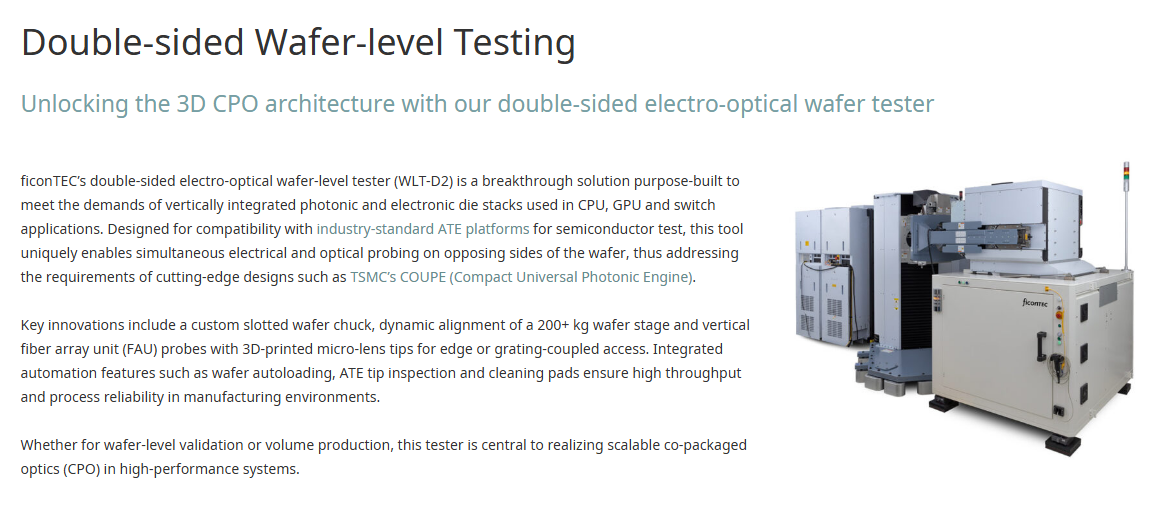
Source: ficonTEC
According to SemiVision’s research, wafer-level testing of a 12-inch PIC wafer can take up to 12 hours for the PIC portion alone. Developing faster and more scalable PIC testing methods will therefore be critical to determining whether silicon photonics can achieve true high-volume manufacturing.
From a supply-chain perspective, competition in SiPh and CPO will not be limited to foundries, photonic chip companies, or module manufacturers. It will evolve into competition between complete testing ecosystems.
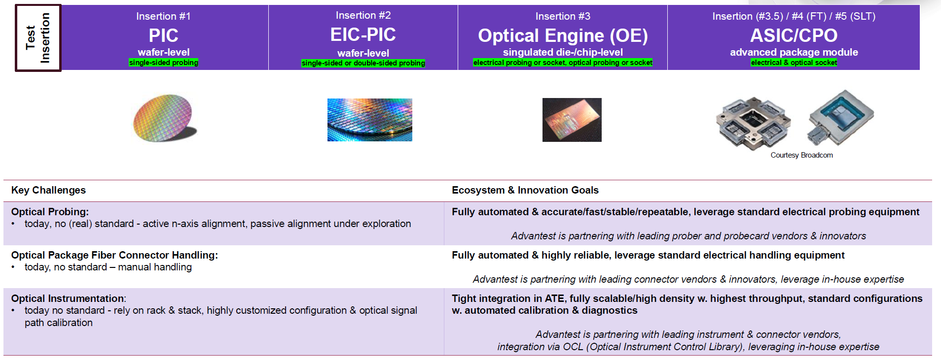
Advantest has outlined four key directions: Automation, Collaboration, Innovation, and Standardization. Its presentation clearly states that the industry needs to use standard electrical probers and handlers, combined with automation capabilities that support wafer and chip handling, as well as probecard and loadboard handling. These systems must then be integrated with standard ATE and high-density optical instrumentation to create a fully integrated test cell.
This means that the future barrier to high-volume SiPh and CPO manufacturing will shift from “Can the industry manufacture photonic chips?” to “Can photonic chips be tested using semiconductor manufacturing methods?”
This is a critical turning point for the industry.
Historically, the optical communications industry has relied heavily on engineering tuning and process-specific know-how. Many manufacturing, packaging, and testing steps remain highly dependent on specialized expertise. This model was viable when module volumes were relatively manageable, product cycles were longer, and specification upgrades followed a more linear path.
AI infrastructure, however, demands a fundamentally different operating model. The AI supply chain requires faster production ramp-ups, greater capacity flexibility, tighter consistency, and manufacturing efficiency that is much closer to the cadence of the semiconductor industry.
The CPO testing ecosystem must therefore converge toward semiconductor manufacturing practices.
This is also an area that Taiwan’s supply chain needs to watch closely. Taiwan has world-leading capabilities in wafer fabrication, advanced packaging, IC testing, and system integration. However, optical testing, FAU alignment, optical probing, connector handling, and optical calibration standards still require much deeper ecosystem-wide collaboration.
For Taiwan to maintain a leading position in the CPO and Optical I/O era, it cannot rely solely on TSMC, packaging houses, or optical module manufacturers. It must simultaneously build integrated electro-optical testing capabilities.

Future test providers will need to measure more than conventional electrical parameters. They must also be capable of performing optical DC, electrical-to-optical, optical-to-electrical, and optical-to-optical testing, as well as modulation characterization, S-parameter measurement, optical loopback testing, and full-system functional validation.
This transformation will gradually reposition test providers from back-end subcontracting partners into an integral part of system-level yield engineering.
CPO testing is not a problem that any single equipment supplier can solve independently.
A complete CPO high-volume manufacturing test cell may involve ATE, probers, handlers, probe cards, DUT boards, optical instrumentation, fiber-alignment units, connectors, sockets, software APIs, calibration models, thermal-control systems, and design-for-test architectures. Any one of these elements can become a bottleneck.
This is why Advantest emphasized in its presentation that, although SiPh and CPO are rapidly emerging, high-volume manufacturing—particularly testing—still faces numerous challenges. The industry requires close collaboration among participants across the testing ecosystem, together with full automation and interoperability among ATE, probers and handlers, probe cards and DUT boards, and auxiliary test instruments.
The significance of this statement goes beyond equipment integration. It points to a fundamental change in the industry’s collaboration model.
In conventional semiconductor testing, customers define the test specifications, ATE vendors provide the testing platform, probe-card suppliers provide the interface, and outsourced test providers execute volume production. In the CPO era, this workflow becomes considerably more complex because test results are closely linked to package design, optical-path architecture, DfT strategy, and fiber-coupling methods.
For example, if the design does not include sufficient optical loopback paths or on-chip monitors, it becomes difficult for back-end testing to quickly isolate the source of a failure. If the package-level fiber-coupling structure is not designed with high-volume testing requirements in mind, handler and socket development becomes extremely challenging. Similarly, if the instrument-control layer lacks standardized APIs, correlation between different test cells will deteriorate.
CPO production testing must therefore be considered from the earliest stages of product design.
Future DfT architectures will no longer be limited to electrical scan chains, BIST, JTAG, or memory testing. They will also need to incorporate optical DfT, optical-path calibration structures, loopback paths, monitor photodiodes, thermal sensing, and automated calibration methodologies.
As a result, CPO testing will become a jointly defined engineering discipline spanning design, manufacturing, packaging, and system integration.
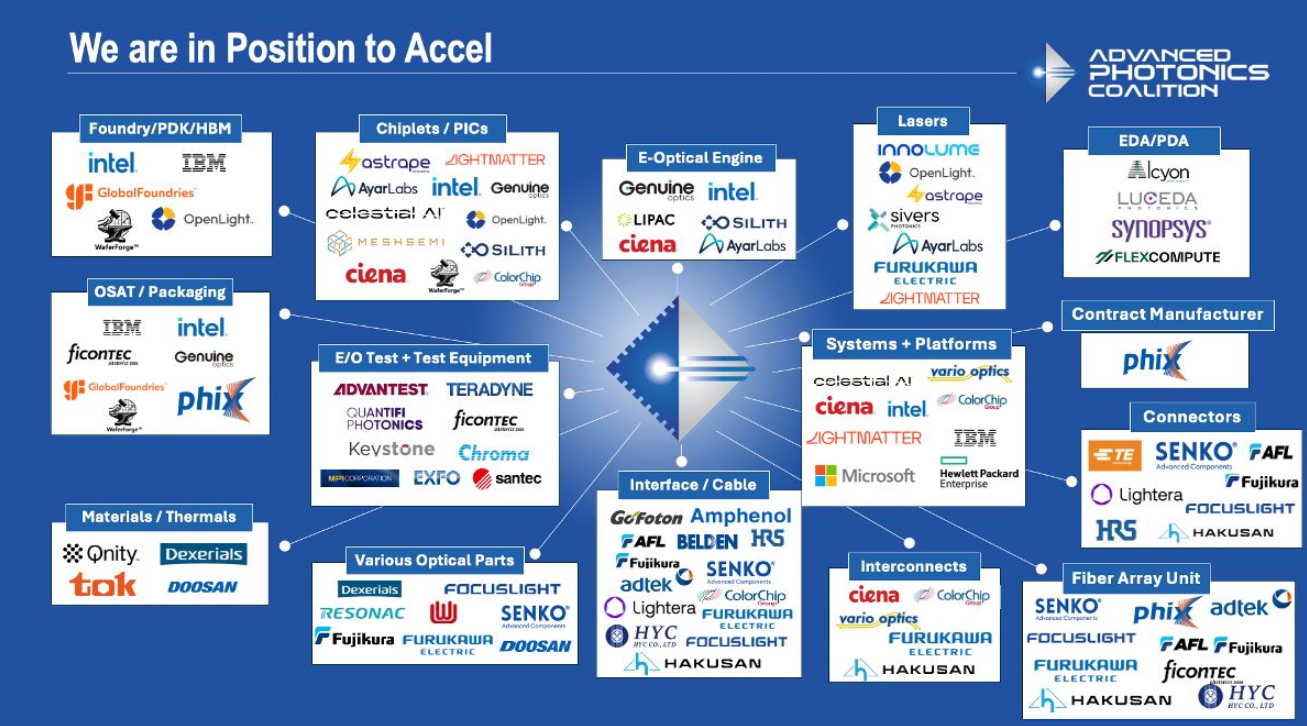
The Advanced Photonics Coalition Open Ecosystem changes and grows every month. We encompass every aspect of the Silicon Photonics + Co-Packaged Optics product formation supply chain, from beginning concept to fabrication. Below is our June 2026 Open Supply Chain Ecosystem as it stands today at almost 60 members.
The technological direction of SiPh and CPO is already relatively clear. However, whether these technologies can be deployed at scale in AI systems will still depend on three critical variables: yield, test time, and test cost.
第二部分:解析(深度解读)
一、这篇文章为什么重要
CPO 话题从去年开始持续升温,市场讨论的重心一直在”光能不能取代铜”“激光器用什么方案”“硅光芯片谁在做”这些话题上。但 TSPA Semiconductor 的这篇文章切了一个非常刁钻但实际的角度:CPO 真正的量产瓶颈不在设计和封装,而在测试。
这个判断与 Advantest(全球测试设备龙头之一)在 SEMICON Taiwan 2025 硅光峰会上释放的信号高度一致。Advantest 毫不掩饰地指出:光测试尚未形成半导体量产的成熟生态,这是 CPO 从实验室走向 HVM 的最大系统性风险。
二、核心论点拆解
2.1 “左移测试”(Shift Left Test)—— CPO 量产的命门
文章的核心概念是 Known Good Optical Engine(已知好光引擎),它是半导体行业”Known Good Die”概念在光引擎上的延伸。
为什么这么关键? 因为 CPO 封装极其昂贵。一旦光引擎被集成进 CoWoS/EMIB/3D IC 级别的先进封装中,任何一个光引擎的失效都可能废掉整个高价值封装体。传统电芯片可以在 wafer sort → final test → burn-in → SLT 链条上逐级筛掉不良品,但光引擎一旦进了封装,光路损耗、耦合效率、偏振漂移、温度敏感性问题就不可修复。
这意味着 测试必须前移,在下游封装发生之前就筛出有缺陷的光引擎。
图例:Advantest 定义的 HVM 测试插入点
| 阶段 | 测试对象 | 目标 |
|---|---|---|
| Wafer-level PIC test | 光集成电路晶圆 | 筛除制造缺陷 |
| Wafer-level EIC-PIC test | 电-光集成晶圆 | 验证光电协同 |
| Singulated-die optical engine test | 单颗光引擎 | 建立 Known Good Optical Engine |
| Final/system-level CPO test | 完整 CPO 封装体 | 系统级验证 |
2.2 三大缺口:光测试 vs 半导体 HVM 的鸿沟
Advantest 指出了三个生态缺口:
光学探针无标准:当前严重依赖主动多轴对准,而半导体量产需要被动对准。光纤与光栅耦合器/边缘耦合器的对接需要精密控制 3D 位置、角度、距离、偏振和温度——这与电探针的标准化程度完全不在一个量级。
光纤连接器处理未标准化:大量工序仍需人工干预。传统 IC handler 可以流利处理 wafer/die/substrate/package,但不擅长处理光纤阵列和高精度光连接器。
光仪表仍在”机架堆叠”时代:依赖定制配置、复杂光路校准,缺少半导体 ATE 那种标准化、多 site 并行、快速校准的生态。
一句话总结:光测试还没有拥抱半导体的量产逻辑。
2.3 12 小时测一张 12 英寸 PIC 晶圆
文中引用的 SemiVision 数据非常触目惊心:一张 12 英寸 PIC 晶圆的晶圆级测试,仅 PIC 部分就可能耗时 12 小时。 这跟传统 CMOS 晶圆的测试吞吐量相比是天壤之别。如果不能大幅加速,硅光就是”造得出来,测不起”的技术。
三、供应链分工重塑
CPO 测试带来一个新问题:谁对光引擎的质量负责? 是硅光 fab?是 OSAT?是光引擎供应商?是 CPO switch 厂商?还是 hyperscaler 自建验证体系?
这不仅是工程问题,更是商业模式问题。如果没有共同行业测试标准,每个客户要求不同的测试项目、校准方法、良率定义、可靠性条件,供应链复杂度会爆炸,CPO 的商业化节奏会被严重拖慢。
未来 CPO 竞争的格局可能变成:谁掌握了测试标准,谁就掌握了良率和成本的话语权。
四、Advantest 的四大方向:Automation / Collaboration / Innovation / Standardization
Advantest 把这四个词放在一起不是随便说的。背后逻辑是:
- Automation:把标准 electrical prober + handler + 自动化 wafer/chip 处理能力拉入光测试
- Collaboration:ATE + prober + handler + probe card + DUT board + 光仪表 + 光纤对准 + 连接器 + socket + 软件 API + 校准模型 + 热控 + DfT——缺一环就会成瓶颈
- Innovation:光学 DfT(design-for-test)架构、片上监控、loopback 路径、自动校准方法
- Standardization:光探针标准、光纤连接器处理标准、仪表 API 标准
五、与本站其他 CPO 系列文章的连接
- The Illusion of CPO [CPO Special Final] 从 scale-up/scale-out 双域、铜墙、六大瓶颈拆解了 CPO 全貌。本文恰好补上了那篇”测试环节”的深度缺失。
- Silicon Photonics Link Budget and Optical Nonidealities 从光链路预算和损耗角度切入;本文则告诉你这些非理想因素在大规模量产场景下如何被量测和管控。
- Lasers for CPO/NPO (Part 1 & 2) 讨论光源方案;本文的光测试体系涵盖了激光稳定性、温度漂移等光源级参数的批量验证需求。
把这些文章串起来,CPO 投资的全景图才完整:设计→封装→光源→链路→测试,缺一不可。
六、投资意义
- 测试设备是 CPO 量产的”铲子公司”:Advantest(ATE)、ficonTEC(光耦合封装设备)、PI(精密对准)等公司将在 CPO HVM 测试生态建设中扮演关键角色。
- OSAT 和测试服务商的竞争格局可能重塑:能够同时提供电学和光学测试能力的 OSAT 将获得定价权。
- 谁定义测试标准,谁定义产业节奏:TSMC 在先进封装领域有巨大话语权,但光测试标准(尤其光学探针、光纤连接器处理)目前尚未形成公认标准——窗口期意味着格局未定。
- 12 小时/晶圆是个需要被技术突破解决的数字:任何能大幅缩短 PIC 晶圆测试时间的技术方案(被动对准、多 site 并行光测试、片上自检)都是关键变量。
七、风险提示
- CPO 整体量产时间表存在不确定性:即使测试问题解决了,封装良率、激光可靠性、热管理等仍然是耦合变量。
- 本文讨论的测试瓶颈主要面向 HVM 大规模量产场景;在 NPO(近封装光学)等中间方案成为主流的过渡期内,测试要求可能有所降低。
- 光测试标准化是多方博弈过程,短期可能分散资源、增加供应链摩擦成本。
以上解读基于原文信息整理,不构成投资建议。CPO 产业链尚在快速演进中,建议持续关注测试标准化进程和主流设备商的布局动向。