Advanced Packaging Co-Design: The Thermodynamic and Mechanical Constraints of High Power GPUs — 先进封装协同设计:高功耗 GPU 的热力学与力学约束
Silicon Code (Chad) 从 ECTC 2026 与《Hybrid Bonding, Advanced Substrates...》一书出发,拆解高功耗 GPU 先进封装协同设计所需的热力学与力学第一性原理:三种传热机制、热阻欧姆类比、应力-应变、CTE 失配与翘曲。英文原文(免费段,含 Figure 1–6)+ 中文深度解读。付费段(翘曲三大来源/四种失效模式/耦合建模/缓解方案)未含。
本文整理自 Chad(Silicon Code / siliconcodesign.com,Substack),原文发布于 2026-06-17(标题原文:Advanced Packaging Co-Design: The Thermodynamic and Mechanical Constraints of High Power GPUs)。 结构为 正文(英文原文,免费段)+ 解析(中文深度解读),方便中英对照阅读。 ⚠️ 付费墙说明:原文大纲中以 🔒 标记的内容(翘曲三大来源、四种常见失效模式、跨耦合失效建模挑战、翘曲缓解方案)位于付费墙之后,本次抓取的公开段止于 Figure 6 与 “after the paywall” 提示句,付费深解未含,未做翻译/改写。如需完整内容请在 Substack 订阅原作者。 来源说明:内容经 Substack 公开页面(jina 阅读器)获取,仅公开段可读;本发布保留完整英文原文并附中文深度解读,仅作信息整理与学习用途,著作权归原作者所有,建议在 Substack 支持原作者订阅。
第一部分:正文(Original Article)
Advanced Packaging Co-Design: The Thermodynamic and Mechanical Constraints of High Power GPUs
Chad · Jun 17, 2026
At ECTC 2026, TSMC noted that many package designers are being too aggressive with their package designs and that a lot of communication is needed to balance the design performance with the manufacturing and reliability constraints of the package.
This post helps reduce that communication overhead.
In this post I’ll be diving into the key mechanical and thermal factors needed for co-designing advanced packaging for high power. The outline of this post is as follows:
- I will explain the current I-shaped paradigm in most technology companies and why engineers will need to embrace T-shaped skillset to effectively co-design tightly integrated systems
- I’ll discuss the key challenges that GPUs are placing on both the package and circuit side
- Then I’ll discuss two fundamental concepts and associated material properties for successful co-design of sub-components with advanced packaging:
- Thermodynamics, including the three sources of heat transfer and thermal resistance
- Stress-strain and associated material properties such as CTE
- Then I’ll describe the:
- 🔒 Three main sources of warpage
- 🔒 Four common failure modes
- 🔒 Challenges with modelling cross coupling failure modes
- 🔒 Last, I’ll discuss a few warpage mitigation options
The research from this post comes from both from my conference experience at ECTC and the book “Hybrid Bonding, Advanced Substrates, Failure Mechanisms, and Thermal Management for Chiplets and Heterogeneous Integration” (2025). I found this book to be a useful mix of both high-level fundamental overviews of advanced packaging and current in-the-weeds academic research on key areas related to packaging.
I previously wrote a masterclass post on the fundamentals of advanced packaging that covers what packaging “is”. This post builds off that by covering the physics dimension when it comes to CTE, warpage, and failure modes. I recommend you read that post along side this one to build a more complete view of advanced packaging.
First I want to describe what I believe effective hardware co-design requires.
Currently, most engineers at major tech companies operate in the “I” shaped paradigm where engineers are highly specialized in their field of choice, and interface with other engineers through requirement specifications and handoff at interfaces.
As systems start become more tightly coupled across domains, many leaders are calling for more cross domain awareness and co-design. However, I believe that most engineers in the “I” shaped paradigm treat co-design as more frequent and earlier meetings.
I believe that effective co-design requires you to become more ‘T” shaped, that is, depth in one domain and breadth in others. This requires you to build a semi-independent knowledge base of high level concepts in other domains to be able to intuitively assess how factors from your domain affect others. This allows you to anticipate issues and ask key questions from domain experts early on.
Becoming T shaped is actually quite difficult to do in an I shaped paradigm, both cognitively and organizationally. Vikram Sekar described these challenges best when he gave career advice because often times, it might be possible to “step” on adjacent teams who are CTA.
I totally understand this, and I’m not saying you should ignore your orgs politics. In any case, here is my blueprint for people who want to become more “T” shaped:
Effective co-design across multiple domains requires you to first ground yourself in the fundamentals of domains that relate to each other in some way. This requires deep work to analyze the technical fundamentals in domains adjacent to your own.
For me, the bulk of my co-design posts revolve around four interconnected domains in hardware:
- On-chip mixed signal (SerDes architecture, ADC, PLL)
- High speed communications (Optical, high speed wireline, and signal integrity)
- Power integrity / management
- Advanced packaging
Each specialty has their own unique set of tradeoffs, such as:
- Gain vs bandwidth in Analog
- Interconnect distance vs BER in SI
- Switching frequency vs ripple vs loss in Power
- Substrate area vs bump stress in Packaging
Understanding the fundamentals in each domains is not an easy process because it requires to you sort through domain specific knowledge from experts and try to extract out the important insights. I found that the tutorials at the beginning of the conferences are excellent at providing a framework to understand more complex conference material that build upon the tutorial material; these are what the tutorials are specifically made for. That way, when I read dense technical papers or conference digests, I can efficiently filter through information that doesn’t matter. I find that the bulk of the writing in conference papers is really dancing around the nuances of previous works while making claims of proposed solutions.
I’m not saying you should become an expert in domains outside of your own; that is overkill for practical purposes. However, I do think you should work backwards to figure out what baseline knowledge you need to understand more domain-specific knowledge from other people.
Then, after understanding tradeoffs in each domain, try to understand how effects from each domain “couple” to other domains. Based on my previous writing, these are some interactions I can think of off the top of my head:
- Power supply induced jitter and crosstalk lower BER of the signal path
- Fast current transients in AI workloads cause localized joule heating that can worsen reliability
- Ring modulators in optical communications are sensitive to thermals that need to be corrected with heater feedback loops
Understanding interactions is quite tricky that I admittedly don’t really understand fully quite yet and am trying to understand better myself.
As a start, I recommend people first ground themselves in ONE field. Power and packaging are excellent interdisciplinary fields to start for anyone involved in semiconductors in anyways. I have several posts that provide a good starting point.
Then, to really test if you have the knowledge, try to teach it to others, whether that be through writing or a seminar. This way, others can mutually benefit from the insight in your own process of becoming more T shaped. It’s quite easy to fool yourself in thinking you know something from reading someone’s article until you go and sit down and explain that topic to another person.
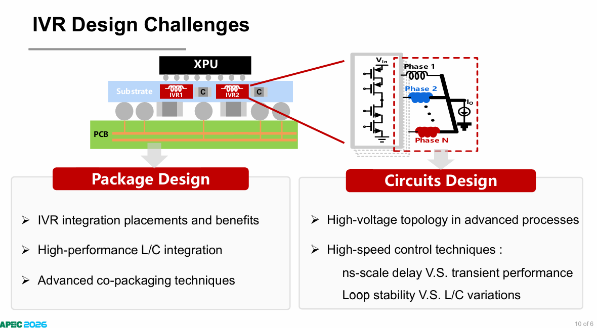
Figure 1. Package and Circuit Challenges for IVR Design. Source: Yuan, J et al. (University of Science and Technology of China) “48V Power Delivery for AI Computing Systems: IVR-Oriented Architecture and Topology Selection” APEC 2026
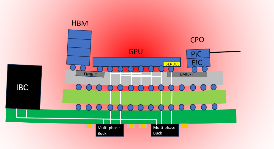
GPU roadmaps are projecting a huge increase in computational power that comes with higher performance requirements, including:
- High power usage. GPUs draw huge current density that is lost in the PDN and dissipates heat.
- High transient response. The critical frequency band of AI workload transients is between ~0.1-10 MHz, and the PDN needs to provide low enough impedance at these frequencies to meet the on-chip droop specs. This is typically done by placing localized decoupling capacitors as close to the chip as possible.
- Large Area. More GPUs per package increase the package area that increases the Distance to the Neutral Point (DNP).
To meet these performance demands, innovations are both needed on the package and circuit design side.
On the circuits side, much work has been done on optimizing specialized power conversion topologies such as multi-phase buck/TLVRs at the PoL and LLC DCX for the IBC. I dive deep into these fundamentals of the circuit architectures in more detail:
On the packaging side, there are several well established failure mechanisms and integration techniques. I briefly touched upon these in these posts:
The issue with high power is that they stress the package, enhance the already established failure mechanisms, and opens up possibilities for new ones. Large BGAs with up to 2000 - 6000 balls face mechanical challenges with heavy heat sinks and continuous vibration.
Lets dive deeper into important packaging considerations.
Co-design of the high power with the package involves knowledge of fundamental concepts in thermodynamics and stress-strain. These are pretty well known to people in those domains and I realize there’s a lot more depth underneath these equations I am simplifying.
As an EE myself who is more specialized on the circuit side, I’m framing these as high level mental models for people outside of these domains to have a first order understanding of the mechanical and thermal effects of packaging.
Likewise, if you are very familiar with these but not familiar with those concepts on the electrical side like signal integrity, power electronics, or the intricacies of high speed SerDes, well, lucky for you, I have mental models on those on my Substack as well that are linked throughout this post.
Conduction
Conduction is heat transfer within a stationary solid, liquid or gas due to temperature differences. Energy is “diffused” from more energetic regions to less energetic particles.
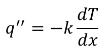
Conduction is governed by Fourier’s law:
\[q'' = -k \cdot \frac{dT}{dx}\]where
- $q’’$ is the heat transfer per unit area (W/m²)
- $k$ is the thermal conductivity of the material (W/m·K)
- $dT/dx$ is the temperature gradient (K/m)
Common values for thermal conduction range from:
- 0.024 (air),
- ~0.2 - 0.35 (for epoxy, polymide, and FR4)
- 120 (silicon)
- 390 (copper)
Conduction matters when dissipating heat from:
- The GPU - Rubin generates 1,800W to 2,300W per GPU
- Joule heating in the interconnects - this is self-heating due to IR drop that increases as current density increases
Convection
Convection refers to heat transfer between a surface and a moving fluid at different temperatures
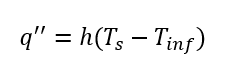
Convection is governed by Newton’s law of cooling:
\[q'' = h \cdot (T_s - T_\infty)\]where
- $q’’$ is the heat transfer per unit area (W/m²)
- $h$ is the convective heat transfer coefficient (W/m²·K)
- $T_s$ is the surface temperature of the solid (K or °C)
- $T_\infty$ is the temperature of the surrounding fluid far from the surface (K or °C)
Convection can be classified either as free (such as hot air rising from a heater) or forced (such as cooling a CPU with a fan).
Common values for convective heat transfer coefficient include:
- Free: 2 - 25 for gasses and 1000 for liquids
- Forced: 25 - 250 for gasses and 100 - 20,000 for liquids
Convection cooling can be facilitated through the use of heat sinks, liquid cooling or immersion cooling with single and two phase variants.
Radiation
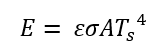
Radiation is the transfer of thermal energy through EM waves without a need for a medium. It is governed by:
\[E = \varepsilon \cdot \sigma \cdot A \cdot T_s^4\]where
- $E$ is heat transfer rate of emission (W)
- $\varepsilon$ is the emissivity of the surface (between 0 to 1)
- $\sigma$ is the Stefan-Boltzmann constant (5.67e-8 W/m²·K⁴)
- $A$ is the surface area of the radiating body
- $T_s$ is the absolute temperature of the surface (K or °C)
Compared to conduction and convection, radiation is not a primary heat transfer mechanism for ground based AI data centers, but could potentially be a dominant heat mechanism for space based AI data centers. We’ll see how that plays out.
Note that radiation also includes the absorption of incident radiation, so the net heat transfer depends on the balance between the inflow and outflow of radiation.
Fundamentally, for a GPU to maintain a thermal equilibrium below a threshold temperature, the conduction and convection equations must be in balance with each other for the cooling system to handle the heat dissipation of the GPU and subsystems.
Of course, there are many other factors such as boundary conditions, unique material properties, and CPU loads that are important and must be taken into account. If, for whatever reason, the heat removal becomes a bottleneck of GPU performance, then tricks need to be played on the SW side to manage the workload until the cooling or packaging system is able to catch up.
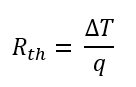
Thermal resistance quantifies the opposition to heat flow at any two points where there is a temperature difference. It is given by
\[R_{th} = \frac{\Delta T}{q}\]where
- $R_{th}$ is the thermal resistance (K/W or °C/W)
- $\Delta T$ is the temperature difference between two points (K or °C)
- $q$ is the heat transfer rate (W)
Figure 2. A simplified Chip Package with each layer modelled as an equivalent thermal “resistance”. Adapted from Fig 8.6, 8.7, John Lau and Xuejun Fan. “Hybrid Bonding, Advanced Substrates, Failure Mechanisms, and Thermal Management for Chiplets and Heterogeneous Integration”
Thermal resistance is a convenient first order approximation because it almost resembles an Ohms law analogy to heat transfer, with analogous parameters:
- Electrical current is the heat transfer rate
- Electrical resistance/conductivity is thermal resistance/conductivity
- Electrical potential is the temperature
Heat sink fins can be modelled approximately using this model to estimate heat transfer. Of course, this approximation is valid if the thermal “circuits” are contained within a lumped approximation, where the heat flow is uniformly distributed in confined materials. Anything that is distributed or highly coupled will require sophisticated modelling.
Figure 3. Material deformation when stress is applied
All materials with a PCB stack experience strain / material deformation under some kind of loading. There are two major categories of materials:
- Ductile material - A material that initially deforms linearly as more stress is applied, then after a certain threshold, it undergoes plastic deformation over a wide range until it ultimately fails. This is the dynamic when you pull hard taffy or gum. Most metals fall into this category.
- Brittle materials - Brittle materials show a steep linear curve with a sharp fracture at the top. Glass falls into this category.
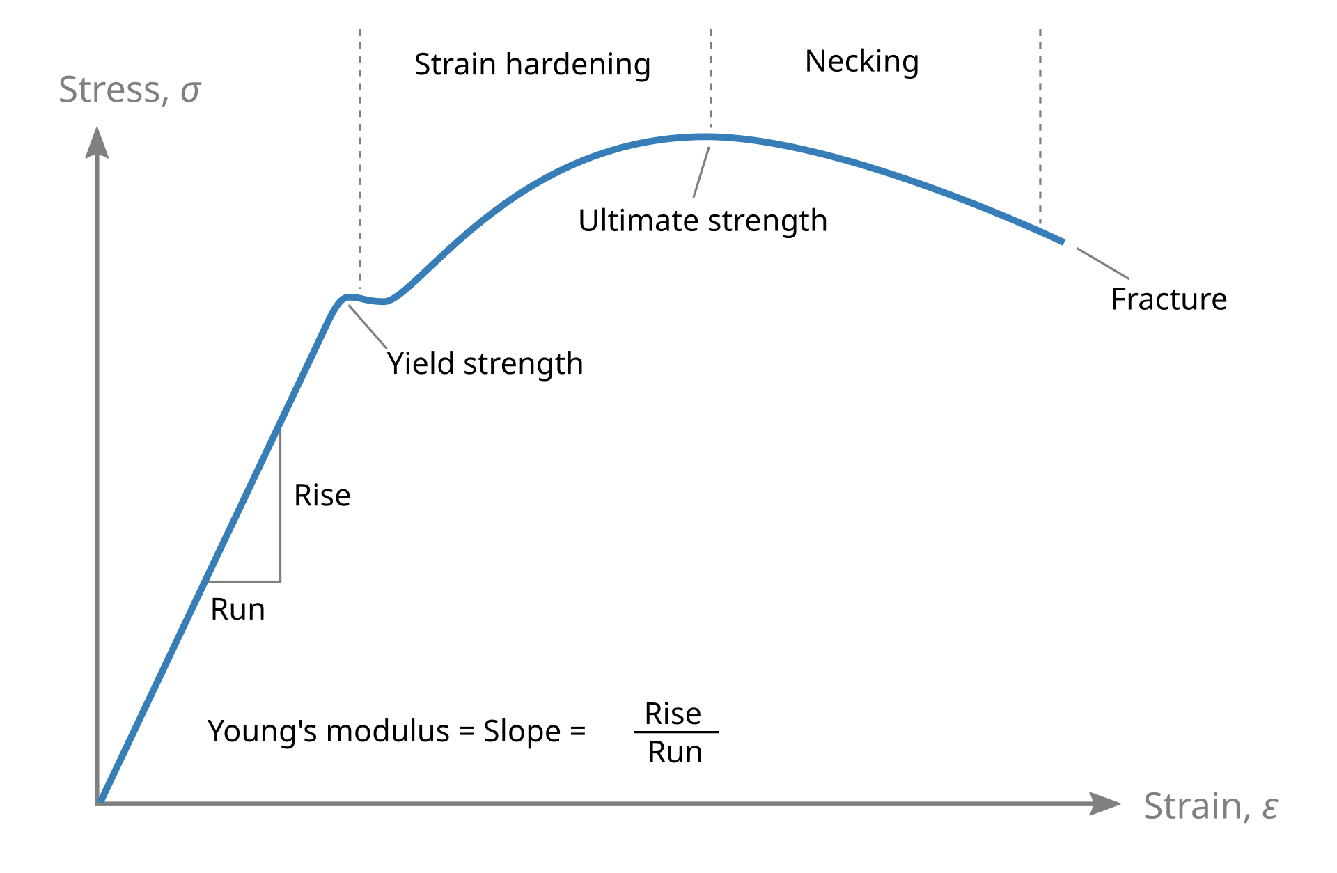
Figure 4. Stress strain curve for a ductile material. Source: https://en.wikipedia.org/wiki/Stress%E2%80%93strain_curve#/media/File:Stress_strain_ductile.svg
For ductile material, the left most region is governed by Hooke’s law which describes material deformation in the elastic region. It is given by
\[\sigma = E \cdot \varepsilon\]where
- $\sigma$ is the average normal stress across a cross section area of a material
- $\varepsilon$ is the average normal strain, given by $(L - L_0) / L_0$
- $E$ is the modulus of elasticity (or Youngs modulus)
On the right side of the linear region, the material starts deforming and ultimately fails to a fracture. Of course, we hope that packaging materials don’t enter this region, but performance requirements can make it difficult to design around this.
Figure 5. Shearing Force
Another form of strain, shearing, changes the angle between two normally perpendicular lines of a material. It is given by:
\[\tau = G \cdot \gamma\]where $\tau$ is the shear stress, $G$ is the shear modulus, and $\gamma$ is the shear strain.
Bumps in between package layers experience both shearing and compressive / tensive forces.
There are a few material properties that matter:
- Youngs modulus - Describes the ability for a material to resist deformation when subjected to stress. Typical values include:
- 6 for underfill epoxy
- 8 - 22 for FR4
- 131 for silicon
- 132 for copper
- Poisson’s ratio - the ratio of the strains in the axial direction and the lateral direction. The max value is 0.5. Typical values include:
- 0.1 - 0.14 for FR4
- 0.28 Silicon
- 0.35 for copper
- Creep - a time dependent permanent deformation of a material under a constant load or stress at a constant temperature. Creep is common at elevated temperatures.
- Stress relaxation - a gradual decrease in stress by a material under a constant strain over time.
- Viscoelasticity - a nonlinear, hysteretic curve to loading and unloading where a material recovers its shape over time after unloading
- Viscoplasticity - when a material suffers permanent, rate-dependent plastic deformation that does not recover
- Viscoplasticity is important when describing the behavior of solder since it is subject to strain and creep deformation.
- One popular viscoplasticity model of solder is the Anand model that governs the rate of change of the inelastic strain. It takes multiple effects such as strain rate sensitivity and deformation resistance into account.
- Coefficient of Thermal Expansion (CTE)
- CTE is perhaps one of the most important and most talked about material properties for packages because it describes material behavior at the interface of thermal and mechanical properties.
- CTE is a form of material “strain” where an increase in temperature causes the material to expand, and a decrease causes it to contract. It is given by:
where
- $\varepsilon_{th}$ is the strain due to temperature with no mechanical load
- $\alpha$ is the coefficient of thermal expansion
$\Delta T$ is the change in temperature
- Common CTE values include:
- 2.6 for silicon
- 17 for copper
- 20, 70 for epoxy
- FR4:
- 10, 15 in plane
- 65, 180 in z-axis
- For any given package size, material with a higher distance from the neutral point will experience higher deformation since it elongates / contracts more, thus increasing the stress on solder joints in that area.
Figure 6. How CTE mismatch of two connected materials cause warping due a difference in length deformation when a high temperature is applied
Now that I’ve established some thermal and mechanical fundamentals, we can discuss how these play a role in warpage, and failure modes after the paywall.
🔒 付费墙提示(本发布未含):原文在此之后的内容——翘曲的三大来源(Three main sources of warpage)、四种常见失效模式(Four common failure modes)、跨耦合失效建模挑战(Challenges with modelling cross coupling failure modes)、翘曲缓解方案(warpage mitigation options)——均位于 Substack 付费墙之后,本次公开抓取未获得,故不做翻译或改写。如需完整深解,请在 Silicon Code (siliconcodesign.com) 订阅原作者。
第二部分:解析(深度解读)
一、核心论点摘要
这篇文章解决的是一个非常”工业界”的问题:在 ECTC 2026 上,TSMC 公开指出很多封装设计者把封装方案做得过于激进,要在设计性能与制造/可靠性约束之间反复沟通、反复返工。作者的目的,是用一篇”协同设计(co-design)物理手册”来降低这种沟通成本。
文章分两层推进:
- 组织/认知层:提出 I 型 → T 型工程师 的转型框架。传统大厂工程师是”I 型”——在自己领域极深,靠接口文档和交接与其他人协作;但在系统跨域耦合越来越紧的今天,需要”T 型”——一域有深度、多域有广度,才能提前预判跨域问题、向领域专家提出关键问题。
- 物理层(本文免费段主体):把高功耗 GPU 先进封装协同设计必需的热力学(三种传热 + 热阻)与力学(应力-应变 + CTE 失配)第一性原理,讲成一套”高层心智模型”,让电路侧工程师也能建立一阶直觉。
作者反复强调:自己是个偏电路侧的 EE,所以把这些机械/热学内容刻意简化成类比和数量级,方便跨域者上手;而完整的翘曲、失效模式、缓解方案在付费段。
二、T 型工程师框架解读
- 四大互联硬件域:片上混合信号(SerDes/ADC/PLL)、高速通信(光/线速/信号完整性)、电源完整性与管理、先进封装。这恰好是当下 AI 硬件最关键的交叉带。
- 每个域的”权衡三角”:模拟的增益 vs 带宽、SI 的互连距离 vs BER、电源的开关频率 vs 纹波 vs 损耗、封装的基板面积 vs bump 应力。理解这些权衡,是跨域对话的共同语言。
- 跨域耦合实例(文章举得很妙):电源噪声引起的抖动和串扰会拉低信号路径 BER;AI 负载的快速电流瞬变造成局部焦耳热、恶化可靠性;光通信里的环形调制器对温度极敏感、需 heater 反馈环校正。这些都说明——单域优化往往以另一域恶化为代价。
- 落地建议:先在一个域打深(作者推荐从 Power 或 Packaging 切入,因为跨域性最强);再用”教别人(写作/seminar)”来检验自己是否真懂。能讲清楚,才算真懂。
这个框架与本站一贯主张一致:CPO、硅光、先进封装从来不是单点技术,而是”光电热力”耦合系统。读懂跨域耦合,才读得懂产业。
三、关键物理概念解读(一阶直觉)
1. 三种传热机制 | 机制 | 公式(一阶) | 数量级 / 备注 | |—|—|—| | 传导 | $q’’ = -k\,dT/dx$ | 硅 $k≈120$、铜 $≈390$、环氧/FR4 $≈0.2–0.35$、空气 $0.024$(W/m·K) | | 对流 | $q’’ = h\,(T_s−T_\infty)$ | 强迫气体 25–250、液体 100–20000(W/m²·K);靠散热器/液冷/浸没(单相/两相) | | 辐射 | $E = \varepsilon\sigma A T_s^4$ | 地面数据中心非主机制;太空 AI 数据中心可能是主机制 |
关键点:GPU 要维持在阈值温度以下,必须传导与对流方程相互平衡——冷却系统要兜得住 GPU 与子系统的散热。一旦散热成为瓶颈,就只能靠软件侧”限流/调度的 trick”扛着,直到冷却/封装跟上。
2. 热阻的欧姆类比 $R_{th} = \Delta T / q$,与电路完全同构:电流↔热流、电阻↔热阻、电势↔温度。芯片-封装各层可建模成一串等效热阻。这套类比让电路工程师瞬间有直觉,但也只在一阶集总近似下成立;分布/强耦合必须上复杂仿真。
3. 应力-应变与材料分类
- 延性材料(多数金属):先线性弹性(胡克定律 $\sigma=E\varepsilon$),过阈值后大范围塑性变形直至断裂(像拉软糖)。
- 脆性材料(玻璃):陡直线 + 顶部脆断。
- 剪切应变 $\tau=G\gamma$:封装层间 bump 同时承受剪切 + 压缩/拉伸力,这是失效的高发区。
4. CTE 失配 → 翘曲(文章免费段的压轴) CTE 是封装里”最被讨论”的材料属性,因为它处在热-力交界处:升温膨胀、降温收缩,$\varepsilon_{th}=\alpha\Delta T$。典型值:硅 2.6、铜 17、环氧 20/70、FR4 面内 10–15 / z 轴 65–180(×10⁻⁶/K)。
距中性点(DNP)越远的材料,伸缩越大 → 该处焊点应力越高。两种 CTE 不同的材料相连,高温下长度变形不一致,就会翘曲(warpage)——这正是 Figure 6 要表达的,也是付费段”三大翘曲来源 / 四种失效模式”的物理起点。
四、与本站其他文章的衔接
- 先进封装 / CoWoS 系列:本文是”封装为什么难”的物理地基;本站 CPO、硅光封装文章可在其上叠加”光-电-热-力”耦合视角。
- CPO 与光测试系列(如《CPO 的最大瓶颈不是光学,是量产测试》):高功耗 + 翘曲/应力,正是 CPO 把光学塞进封装后测试与良率难的根因之一。
- 热管理 / 散热材料:Rubin 单 GPU 1800–2300W 的量级,直接驱动液冷、浸没冷却、热界面材料、low-CTE 基板的需求。
- 信号完整性 / 电源完整性:文中”电源噪声→抖动→BER”“瞬变电流→焦耳热→可靠性”是本站 SI/PI 文章的跨域注脚。
五、产业与投资视角(个人观点,非建议)
- 高功耗 GPU(Rubin 1.8–2.3kW)把”热-力”推到前台:先进封装不再只是互连密度问题,而是可靠性与可制造性问题。能解决翘曲、应力、热阻的材料与工艺(low-CTE 基板、underfill、混合键合、液冷/浸没、热界面材料)价值抬升。
- 异构集成(chiplet)的隐性门槛:本文引用的《Hybrid Bonding, Advanced Substrates, Failure Mechanisms, and Thermal Management…》一书,正是把”混合键合 + 热管理 + 失效机制”打包成系统议题——这指向封装级系统集成能力会成为晶圆厂/OSAT 的分水岭。
- 测试与良率:翘曲/应力直接转化为量产测试与良率挑战,呼应本站对”光测试/晶圆级测试”机会的判断。
- ⚠️ 风险提示:本文付费段(翘曲来源、失效模式、缓解方案)未含,产业结论的”解法侧”尚不完整;文中数量为作者引用的典型值,具体项目以厂商公开资料为准。本解读仅为信息整理与学习,不构成任何投资建议。
六、结语
这篇文章的价值,不在某个公式,而在把”封装协同设计”翻译成跨域工程师都能用的共同语言:先当 T 型人,再用量级和类比建立一阶直觉,最后用仿真兜底。免费段把”热-力”地基打得很扎实;想看翘曲与失效的”解法”,得去原站付费段。
原文:Chad, Silicon Code (siliconcodesign.com),2026-06-17。英文原文经公开页面整理,著作权归原作者所有。