AI Chiplet Architectures Redefining Test Insertions — AI Chiplet 架构如何重定义测试插入点
SemiEngineering 对 AI chiplet / 2.5D-3D 异构集成如何把质量保障从单 die 推向 CoW/CoP 模组级、并重定义测试插入点(metrology/ATE/SLT 分层策略)的技术解读,附 Teradyne 四张架构图。
原文来源:SemiEngineering|作者 Jeorge Hurtarte|原文发布于 2026-08-11 本文为「英文原文 + 中文深度解读」两层结构,配图取自原文(Teradyne 提供)。 原文无付费墙,全文已取得。
第一部分:正文(Original Article)
AI Chiplet Architectures Redefining Test Insertions
Heterogeneous integration does not simply increase complexity but redistributes where quality must be assured.
AI drives demand for xPU, HBM, switches, and CPO, but lithographic limits mean monolithic dies can’t keep pace. Instead, the industry is moving to all sorts of complex packages. This creates new challenges for test. Here’s a look at how test vendors are responding.
The challenge: From monolithic die to interposer-based modules
With heterogeneous integration well established and supported by evolving standards, the industry is at a technical inflection point: AI accelerators are no longer constrained primarily by transistor scaling, but by integration strategy and package-level interconnect density. Compute die, HBM stacks, and I/O die are assembled on silicon interposers and, increasingly, in panel formats. This brings into focus new physical realities such as reticle limits (maximum size 26mm x 33mm), microbump pitch, TSV routing, and die-to-die interfaces.
We must recognize the impact of lithographic limits, which dictate how much can be squeezed into a particular die size, when paired with these physical realities. The result is a need for multi-chip designs using 2.5/3D integration packages to create more complex systems. Key test factors are grounded in geometry, pitch, and interconnect density – variables that directly affect probing, access, and test coverage.
Today’s industry trend integrates multiple chiplets and multiple dies. These are stacked either on top of each other like HBMs, or side by side on a silicon interposer used as an interconnect layer. This then moves into the package substrate and then into the circuit board. This complexity presents new test challenges. Once multiple, high-value die are assembled on an interposer, the package architecture itself begins to dictate where and how validation must occur. Teradyne recognizes this as a trend with growth potential for the next decade and is responding with new test solutions. See, for example, Teradyne’s recent press release where Teradyne’s UltraFLEXplus tester is paired with TEL’s Prexa SDP prober for singulated device probing.
Known-good everything: The economic imperative
High-value AI accelerator companies change test strategies and test insertion steps based on economic drivers. With the average selling price of a data center GPU rising to about $28,000 by 2030, high scrap costs mean singulated die test, stack validation, and interposer module verification are not optional. Computing and networking devices must be tested, and test coverage is tied directly to yield and quality protection.
At the system level, complexity scales rapidly. A single AI data center rack can integrate hundreds of GPUs, thousands of memory devices, and multiple high-speed switches, all interconnected through dense chiplet-based architectures. Each GPU itself is no longer a monolithic device, but a heterogeneous assembly of compute die, stacked HBM, and high-speed I/O, and even photonics interconnect, creating thousands of interconnects.
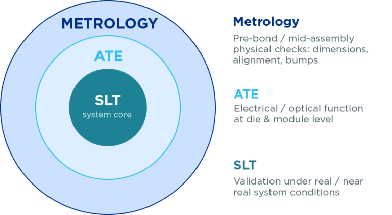
This complexity is amplified by the integration of co-packaged optics (CPO), where optical engines (often deployed in arrays of dozens per system) are placed alongside compute silicon to enable high-bandwidth, low-power data movement. Because these optical engines are multi-die subsystems combining electronic and photonic components, they must be validated as known-good optical engines before integration. A single defective component can compromise the entire system. The underlying goal is supporting the shift toward “known-good everything”, with metrology, ATE (automated test equipment), and SLT (system level test) combining to form a layered quality strategy.
For example, by identifying physical defects at early stages (pre-bond and mid-assembly), metrology helps prevent faulty components from being integrated into expensive multi-die packages, where failures would be far more costly. As a result, its role is expanding alongside advanced packaging, becoming an essential step in improving yield, reducing risk, and enabling more effective downstream test strategies.
Metrology focuses on physical integrity and verification: are the structures built correctly? It measures dimensions, warpage, alignment, and interconnect quality (e.g., microbumps, TSVs, spacing) and often uses optical or x-ray inspection to catch defects during and immediately after assembly steps. This happens pre-bond and mid-process, before full electrical validation. ATE, by contrast, verifies electrical and optical functionality and performance at the device or module level, ensuring the chip or package behaves as intended. Then SLT validates the device in a real or near-real operating environment, catching issues that only appear under system conditions, or “mission mode”, and validating the device works in the overall system.
Module-level probe: A structural shift
There are practical implications for probing large interposer-based modules before substrate attach. This includes mechanical scale, current delivery, power dissipation, contact integrity, probe force, and thermo-mechanical warpage stability at probe. Overall, the more chips tested, the more power consumed (into thousands of watts).
More complexity and more chips also introduce possible new areas for defects. ATE structures must verify the assembly integrity of the chiplet stack, the multiple HBMs, the microbumps, the C4 bumps, and the interconnection before everything is assembled into the interposer and final package substrate.
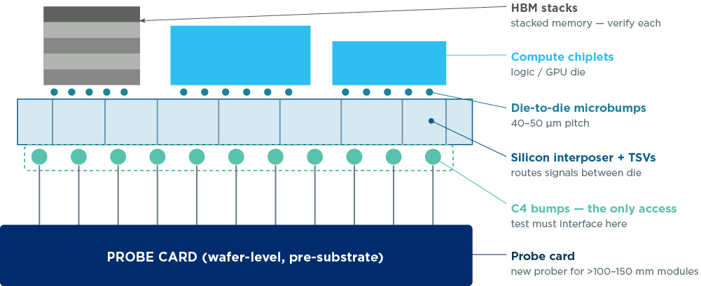
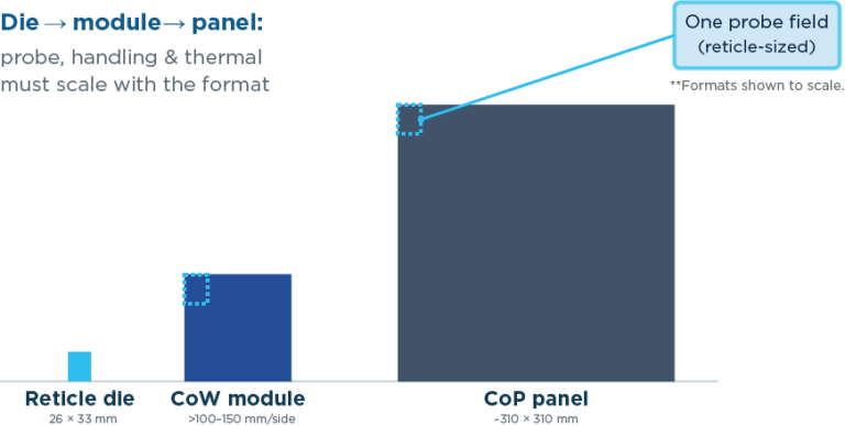
Chip-on-wafer (CoW) module probing introduces a fundamentally new class of test challenge, because the device under test is no longer a single die, but a partially assembled multi-die system on a silicon interposer. At this stage, electrical access is typically limited to C4 bump interfaces, requiring test to be performed before substrate attach using probe-based methods rather than traditional package test. These CoW modules are significantly larger than reticle-limited die—often exceeding 100mm2, 150mm2, or more on a side—which places new demands on probe mechanics, contact uniformity, and test cell architecture.
The probe interface must also support high-current delivery, tight thermal control, and high-speed signal integrity across thousands of fine-pitch interconnects. Ensuring known-good CoW modules requires verification of chiplet interconnects, microbump and C4 integrity, and interposer connectivity—driving the need for new prober designs, advanced DFT strategies such as IEEE 1838, and closer coupling between mechanical, thermal, electrical, and optical test domains.
Test cell architecture must adapt – today’s wafer probes are not suitable, so Teradyne is working with its open ecosystem suppliers to expertly handle larger packages. In parallel, the industry is extending these architectures beyond wafer-based integration toward panel-level formats, or chip-on-panel (CoP). By moving from 300mm wafers to panel dimensions on the order of 310mm × 310mm, CoP improves space utilization and manufacturing efficiency, enabling lower cost per module for large, heterogeneous designs.
However, this shift to CoP amplifies existing test challenges. The larger form factor increases demands on handling, alignment, and probe scalability, while maintaining the same requirement for multi-stage test insertions. CoP also opens the door to alternative interposer materials, including glass and organic substrates, introducing new variables in signal integrity, thermal behavior, and defectiveness.
Together, CoW and CoP shift test from a die-centric model to a module-centric one, where physical scale, interconnect density, and system-level behavior must be validated earlier in the flow.
Fine pitch, hybrid bonding, and access constraints
As advanced packaging brings new test insertions, there are new test challenges related to both access power and active thermal control (for example, on-chip liquid cooling, and new approaches to thermal management). Further challenges result from CPO and integrating optics (for example, fiber alignment).
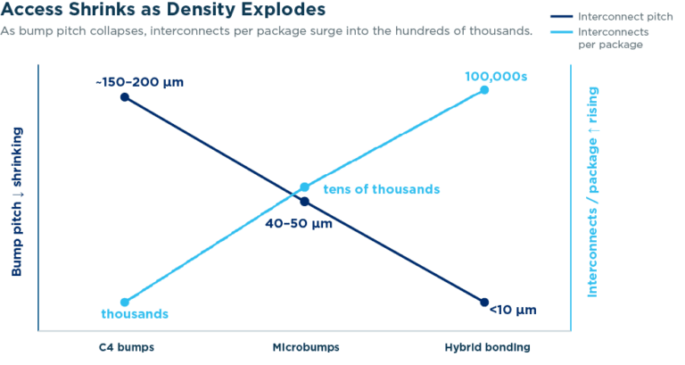
At the physical level, interconnect scaling is tightening, with bump pitches shrinking from hundreds of microns to 40–50µm microbumps, and in some cases moving toward hybrid bonding below 10µm. This significantly increases interconnect density while reducing available probe contact area, making physical access more constrained. The number of interconnects within a package can reach into the tens or even hundreds of thousands, increasing the difficulty of achieving full coverage.
These constraints are compounded by the rise of high-speed die-to-die interfaces, such as UCIe, which operate over short distances with low drive strength and are sensitive to signal integrity and electrostatic effects. As a result, test access must be brought physically closer to the device under test, thus minimizing parasitics and maintaining signal fidelity. Access methodology therefore requires new approaches to probe architecture, interface design, and DFT to ensure that high-speed interconnects can be driven and observed across all insertion points.
For Teradyne, this directly translates into tighter integration between ATE instrumentation and the device interface. This reflects the need for higher bandwidth, lower-noise signal paths, advanced probing solutions, and test cell architectures that can maintain signal integrity at increasingly fine geometries.
Integration density drives insertion density
In summary, the interposer on substrate advanced packaging can be on a wafer format with multiple chips. Eventually, this gets singulated and placed on a substrate. Test leaders must be able to test this at all levels, from wafer level, singulated die, CoW module on interposer wafer tests, singulated CoW module tests, and final assembly.
Heterogeneous integration does not simply increase complexity but redistributes where quality must be assured. Test insertion architectures must evolve alongside package architecture and uncover failures in every step of the process.
References
- xPU refers to computing devices like GPU, CPU, TSU, DPU, LPU, etc.
- Yole Group, 2025
- Metrology in this context can refer to any inspection equipment technology, such as x-ray, optical or SAM.
第二部分:解析(深度解读)
一、核心论点:异构集成「重新分配」了质量保障该发生的位置
这篇文章的题眼其实只有一句话——Heterogeneous integration does not simply increase complexity but redistributes where quality must be assured(异构集成不只是增加复杂度,而是把「质量必须在哪里被保证」重新分配了)。作者 Jeorge Hurtarte(Teradyne 视角)要论证的是:当 AI 加速器从单 die 走向「compute die + HBM 堆栈 + I/O die + 光引擎」的多 chiplet 模组后,传统的「die 级测完再封装」范式已经失效,测试必须从「以 die 为中心」转向「以模组(module)为中心」,并且要把插入点(test insertion)前移到封装流程的早期——在 substrate attach 之前、在中介层晶圆上就把坏件筛掉。
这背后的驱动力不是技术洁癖,而是经济账:文章给出一组关键数字——到 2030 年数据中心 GPU 的平均售价(ASP)将涨到约 $28,000。当一个价值近 3 万美元的高价值模组里塞了多个高价值 die,任何在晚期才发现的一个坏件,都会连累整包报废,scrap 成本变得不可接受。于是 singulated die test、stack validation、interposer module verification 从「可选」变成「必选」。
二、关键概念拆解
1. Known-Good Everything 与三层质量策略。 文章把质量策略拆成三层,这是全文最该记住的框架:
- Metrology(量测):管「物理结构是否造对」——尺寸、翘曲(warpage)、对齐、互连质量(microbump/TSV/间距),常用光学或 X 射线,发生在 pre-bond 与 mid-process,在完整电性验证之前。
- ATE(自动测试设备):管「电性与光性功能/性能」,在 device 或 module 级验证芯片/封装是否按预期工作。
- SLT(系统级测试):在真实或近真实工作环境下验证,专门抓只在「mission mode(任务模式)」下才暴露的问题。
三者的关系是越早筛掉物理缺陷,越能避免把坏件集成进昂贵的多 die 封装——这正是先进封装 yield 提升的核心逻辑。
2. CoW 与 CoP:从晶圆到面板的尺度跃迁。
- CoW(Chip-on-Wafer):在硅中介层晶圆上就把多 die 半成品当 DUT 测,电性访问通常只剩 C4 bump 接口,必须用探针法而非传统封装测试;尺寸常超 100–150mm² 甚至更大,远超 reticle 限制(最大 26×33mm)。
- CoP(Chip-on-Panel):进一步从 300mm 晶圆走向约 310×310mm 的面板级,提升空间利用率与制造效率、降低单模组成本;但尺度放大又放大了 handling/对齐/探针可扩展性难度,并引入玻璃、有机中介层等新材料变量(信号完整性、热行为、缺陷率全变)。
3. 物理极限在收紧。 bump pitch 从数百微米缩到 40–50µm microbump,部分走向 <10µm 的 hybrid bonding;单封装互连数冲到数十万级。互连越密、可探接触面积越小,access 越受限。叠加 UCIe 这类短距、低驱动强度、对 SI/ESD 敏感的 die-to-die 接口,测试访问点必须物理上更靠近 DUT 以压低寄生、保住信号保真度——这要求探针架构、接口设计、DFT(含 IEEE 1838 这类 2.5D/3D 测试标准)深度耦合。
三、与本站其他文章的衔接
- 与 CPO 篇直接互补:本文在「Known-good everything」一节明确指出,CPO 的光引擎(optical engine)本身是电子+光子的多 die 子系统,集成前必须先验证为 known-good optical engine(KGOE)——一颗坏件就能拖垮整系统。这与本站同日发布的《What Will It Take To Deploy CPO At Scale?》里「光互连独特失效模式需链路级 telemetry」形成技术与商业的双拼。
- 与先进封装系列呼应:本站已发过 Intel EMIB vs 其他先进封装、AMD/Qualcomm 新封装等文章,本文的 CoW/CoP、hybrid bonding、UCIe 测试正是那些封装路线的「质量保障底座」。
- 对投资的启示:测试设备(Teradyne、Advantest 等)在先进封装与 CPO 规模化中被「结构性增量」拉动——只要 AI 加速器继续走 chiplet 化与光集成,test insertion 的密度与价值就只增不减。
四、趋势判断与风险提示
- 趋势:测试从 die-centric 走向 module-centric,插入点前移、层数变厚;面板级(CoP)与玻璃/有机中介层是下一站;probe 力学、热控(含片上液冷)、高电流交付、细间距信号完整性成为新护城河。
- 风险:① 探针方案与 test cell 架构跟不上封装尺度/互连密度的速度,会成为良率瓶颈;② CoP 新材料变量(玻璃脆性、有机 CTE)可能引入新缺陷模式;③ 多 die 模组的高价值意味着测试覆盖率不足的风险被放大(一个漏检坏件 = 整包报废)。
一句话总结:AI chiplet 不是把测试「变难」这么简单,而是把测试「重新摆位」——谁能在封装流程最早期、以模组粒度把坏件拦下来,谁就握住先进封装与 CPO 规模化的质量命门。