AMD, Qualcomm Debut New Packaging Technologies — AMD 与 Qualcomm 首发新一代先进封装
整理自 Mark LaPedus(Substack):AMD 与 Qualcomm 同时发布绕开 HBM/CoWoS 瓶颈的新一代内存封装——AMD Versal Premium Gen2 MoP 与 Qualcomm HBC。附英文原文 + 中文深度解读,拆解两条技术路径、关键概念与投资意义。
本文整理自 Mark LaPedus(Substack),原文发布于 Jul 03, 2026(标题原文:AMD, Qualcomm Debut New Packaging Technologies)。 结构为 正文(英文原文)+ 解析(中文深度解读),方便中英对照阅读。 来源说明:内容经公开页面获取;本发布保留完整英文原文并附中文深度解读,仅作信息整理与学习用途,著作权归原作者所有,建议在原站支持作者订阅。 图片说明:原文 Figure 1(Source: Rambus)配图已按原站位置嵌入正文(substackcdn 包装链已解码为 S3 直链并验证可达)。
第一部分:正文(Original Article)
AMD, Qualcomm Debut New Packaging Technologies
Mark LaPedus · Jul 03, 2026
Two companies, AMD and Qualcomm, have separately introduced new memory packaging technologies that address the bandwidth bottleneck issues in today’s systems.
In one announcement, AMD has introduced its Versal Premium Gen 2 Memory on Package (MoP) line. Designed for industrial applications, AMD’s new MoP offering incorporates DRAM and a system-on-a-chip (SoC) all in the same package.
Then, in a separate announcement, Qualcomm recently introduced several AI chip products, including a high-end memory packaging technology called High Bandwidth Compute (HBC). HBC is a 2.5D-like memory technology, which addresses the memory bandwidth issues in AI servers.
The respective packaging technologies from AMD and Qualcomm are different and address different market segments. But both packaging technologies have a few things in common. First, they enable faster data transfer rates with reduced latency in systems. Second, both companies claim that their respective technologies have several advantages over existing high-end memory package types, namely high bandwidth memory (HBM).
Based in Santa Clara, Calif., AMD is a supplier of x86-based processors for PCs and servers, as well as FPGAs. Located in San Diego, Calif., Qualcomm is best known as a supplier of chipsets for smartphones.
Qualcomm also sells ARM-based processors for PCs, putting the company in direct competition against AMD and Intel. Now, Qualcomm is moving into the data center with the introduction of a new CPU and AI chip. AMD, Intel and many others also compete in those markets.
What is packaging?
Before describing the new packaging technologies from AMD and Qualcomm in more detail, let’s attempt to answer a simple question: What is packaging?
Packaging is an important part of the semiconductor industry. In the semiconductor process flow, a company first designs a chip line using specialized electronic design automation (EDA) software tools. Then, a chipmaker (i.e. Intel, Samsung, TSMC, others) manufactures a chip line based on that design in a large facility called a fab.
After the chips are fabricated, the devices are sent to a separate facility. Then, in that facility, the processed chips are assembled into an IC package. Basically, a package is a small and rugged enclosure that protects a chip from harsh operating conditions. More importantly, a package helps boost the performance of a chip.
There is no single package that fits every need. In fact, packaging companies offer many package types. Each one is designed for a specific application. Packaging companies provide various packages for automotive, communications, computing and industrial applications.
Another application—AI–is a hot topic today. In AI data centers, computer systems must process complex AI algorithms at high speeds. To process the data, these systems generally incorporate a powerful AI chip, such as an AI accelerator, GPU or related device. Typically, in a system, an AI chip, along with HMB, are incorporated in the same package. This is referred to as a 2.5D package (See Figure 1).
In HBM, you vertically stack 8, 12 or more DRAM dies on top of each other. Then, the DRAM dies are connected using tiny vertical wires called through-silicon vias (TSVs). The TSVs provide the electrical connections between each die.
In operation, HBM enables the data to transfer between the memory and AI chip at high speeds. HBM employs a 1024-bit memory bus, enabling high bandwidth in systems.
Micron, Samsung and Sk Hynix are the main suppliers of HBM products in the market. All told, HBM is the dominate high-end memory technology for high-end applications like AI.
The problem? DRAM, the memory chip product used in HBM, is in tight supply. Plus, DRAM prices have escalated. Thus, HBM remains in tight supply with high prices. And in many cases, the AI chip and HBM are packaged using TSMC’s 2.5D packaging technology. TSMC’s 2.5D technology, called Chip on Wafer on Substrate (CoWoS), is also in tight supply.
In response, suppliers of memory products are expanding their manufacturing capacities to meet demand. In addition, TSMC is also scrambling to add more CoWoS manufacturing capacity.
Still, thanks to AI, DRAMs are expected to be in tight supply through 2027 and perhaps beyond. This presents a major headache for the entire industry.
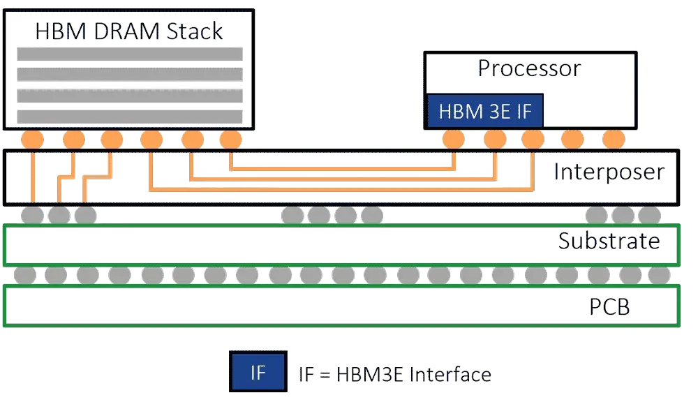
Figure 1. HBM is a DRAM memory stack. HBM is often situated in a 2.5D package. An HBM DRAM stack and a processor or GPU are situated on an interposer in the same package. In operation, HBM enables the data to transfer between the memory and the processor or GPU at high speeds. Source: Rambus
Way of the Dragonfly
The supply chain woes are beyond the control of many. But as before, the semiconductor industry continues to innovate despite the challenges. In fact, some believe that the industry needs new and better packaging solutions.
For example, Qualcomm recently introduced its new Dragonfly chips for AI data centers, including the C1000 CPU, AI300 inference accelerator and a custom silicon offering. The company also rolled out HBC.
In many ways, HBC resembles a 2.5D package with HBM. In HBC, Qualcomm places an AI chip in a 2.5D package. Then, LPDDR DRAM dies are stacked on top of each other, and placed in the same 2.5D package. The AI chip and DRAM stack are side-by-side in the same package, according to a video clip from Qualcomm.
HBC is designed to enable a 6x increase in bandwidth per watt versus HBM, according to Qualcomm. HBC is designed to enable a 200x increase in capacity per watt versus SRAM, according to the company.
Initially, Qualcomm will incorporate HBC within its AI250 data center rack, which is a rack-scale AI inference platform. “Qualcomm says HBC combines accelerator logic with 3D-stacked DRAM in a tightly coupled package,” said Jon Peddie, president of Jon Peddie Research, a research firm, in a blog.
“Qualcomm describes HBC as a memory-centric accelerator architecture. The design keeps data closer to compute, reduces movement across external interfaces, and improves bandwidth efficiency,” Peddie said.
It’s a promising solution. “Qualcomm’s HBC approach puts memory bandwidth, packaging, and power at the center of system design. The inflection point emerges as hyperscalers and enterprises evaluate AI racks through total cost, software portability, and supply resilience. If Qualcomm delivers, AI data centers could support more diverse architectures and reduce dependence on a single software-hardware model,” Peddie said.
Still, there are some unanswered questions about HBC. “Silicon teams will want details on packaging, thermals, yield, repair, memory supplier support, interconnect topology, and compiler visibility. CIOs will focus on rack power, cooling, utilization, procurement timing, cloud access, service support, and software compatibility,” Peddie said.
Commercial sampling of HBC Gen 1 with AI250 is expected in mid-2027.
More advanced packaging
To be sure, AI in the data center tends to grab the headlines these days. But as before, there is a huge semiconductor market beyond data centers. These chip markets, such as automotive, communications, industrial and others, are also important.
Looking to address some of these markets, AMD has introduced the Versal Premium Gen 2 MoP technology. Basically, AMD’s MoP offering combines its Versal chip line and DRAM in the same package. AMD’s Versal is a general-purpose system-on-a-chip (SoC) product line.
In total, AMD’s MoP technology can integrate up to 32GB of LPDDR5X DRAM into a single SoC package, delivering up to 288GB/s of bandwidth in up to 60% less board area.
“AMD places standard JEDEC-compatible LPDDR5X devices on the package substrate alongside the Versal compute die,” Peddie explained in a separate blog. “The short interconnect distances eliminate external memory routing, simplify board design, reduce validation effort, and improve signal integrity. AMD estimates more than 60% board-area savings compared with an equivalent discrete-memory implementation. The company also claims that designers can eliminate months of memory-interface design, simulation, qualification, and board-level validation work.”
AMD’s MoP technology is targeted for embedded and industrial applications. As physical AI, networking, aerospace and defense workloads push more data through ever-tighter space and power budgets, MoP targets the designs that need it most: test and measurement, professional video editing, and VPX systems for secure communications and defense acceleration. VPX refers to a rugged, high-performance embedded computing standard (VITA 46) used in aerospace, defense and industrial applications.
Built for long life cycles and industrial-grade environments, AMD’s MoP solution offers 15-plus-year support to help reduce design risk and protect product roadmaps from HBM’s shorter, data-center-driven refresh cycles.
“The target applications reveal where AMD sees demand emerging. Physical AI systems require local processing of sensor data with minimal latency. Networking platforms need larger packet buffers and faster data movement. Radar and electronic-warfare systems process large datasets in real time. Professional video systems require substantial image buffering and AI-assisted enhancement. Test-and-measurement equipment captures and analyzes increasingly large data streams. Each workload places pressure on memory bandwidth and memory capacity while operating within constrained physical footprints,” Peddie said.
AMD Versal Premium Gen 2 MoP devices will begin sampling at the end of 2026 with production shipments expected to begin in the second half of next year.
Still more packaging
Others have also recently introduced new high-end memory packaging technologies, including High Bandwidth Flash (HBF) and Z-Angle Memory (ZAM).
SK hynix and Sandisk are pushing HBF. Both companies have started the standardization process for HBF.
Meanwhile, SoftBank’s subsidiary, SAIMEMORY, recently signed a collaborative agreement with Intel. The companies plan to commercialize ZAM, a next-generation memory technology designed for high capacity, high bandwidth and low power consumption.
第二部分:解析(深度解读)
一、这篇文章为什么重要
Mark LaPedus 这篇报道表面写的是「两家公司同时发了新的内存封装」,但真正的主线是:当 HBM 与 TSMC CoWoS 同时成为 AI 系统的双重 choke point,系统厂与芯片厂正在各自寻找「绕开 HBM/CoWoS」的内存封装路线。这一点对半导体投资人极其关键——过去两年 AI 叙事几乎被「HBM 紧缺 + CoWoS 产能」锁死,而本文给出的正是这一叙事可能出现分流的信号。
三条值得单独拎出来的逻辑:
供给端倒逼创新。 原文明确指出 DRAM 因 AI 需求「tight supply through 2027 and perhaps beyond」,HBM 价格高企,而承载 HBM 的 TSMC 2.5D 封装 CoWoS「also in tight supply」。当最主流的路线又贵又缺,客户就有动力接受替代方案——这正是 AMD 的 MoP 与 Qualcomm 的 HBC 出现的土壤。
两条路径、两个市场,但同一个本质。 AMD 走工业/嵌入式(把 LPDDR5X 直接放在封装基板上),Qualcomm 走数据中心 AI 推理(类 2.5D 的 LPDDR 堆叠)。市场不重叠,但两者共同指向一句话:把内存尽量贴近计算(keep data closer to compute),用「近存/存算一体」思路取代「远内存 + 高速总线」。
先进封装正在从「配角」变「主角」。 无论是 MoP、HBC,还是文中顺带提到的 HBF、ZAM,本质都是「后摩尔时代靠封装补算力」这一更大叙事的组成部分。这跟本站长期跟踪的 CPO/硅光叙事同源——CPO 也是把光引擎用 2.5D/基板集成到封装里。内存封装与光封装,正在汇成同一条「系统级封装(SiP)重构」的主线。
二、核心论点拆解
三家「高带宽内存方案」的对照,可以用一张表看清差异:
| 维度 | AMD MoP(Versal Premium Gen2) | Qualcomm HBC(Dragonfly / AI250) | 传统 HBM(on CoWoS) |
|---|---|---|---|
| 目标市场 | 工业/嵌入式/防务(长生命周期) | 数据中心 AI 推理(rack-scale) | 高端 AI(GPU/加速器) |
| 内存类型 | JEDEC LPDDR5X(标准件) | LPDDR DRAM 3D 堆叠 | HBM(DRAM 垂直堆叠 + TSV) |
| 封装形态 | 内存 die 与计算 die 并排放置在同一基板 | 类 2.5D,AI chip 与 DRAM 堆叠并排 | 2.5D,HBM 栈 + GPU 置于 interposer |
| 关键宣称 | 最高 32GB、288 GB/s、省 60% 板面积 | 相对 HBM 6× 带宽/瓦、相对 SRAM 200× 容量/瓦 | 1024-bit 总线、成熟生态 |
| 供应商依赖 | 标准 LPDDR5X(多源) | LPDDR(需确定内存供应商支持) | 绑定 Micron/Samsung/SK hynix + TSMC CoWoS |
| 时间线 | 2026 年底 sampling,2027 H2 量产 | HBC Gen1 + AI250 2027 年中 commercial sampling | 已大规模量产 |
几个拆得出的核心论点:
- 「相对 HBM 有优势」是两家共同的营销锚点。 AMD 没直接给倍数,而是用「省 60% 板面积、288 GB/s、32GB」这类工程指标说话;Qualcomm 则大胆给出「6× 带宽/瓦 vs HBM、200× 容量/瓦 vs SRAM」的对比——后者数字很漂亮,但注意是「vs SRAM」而非「vs HBM」的容量对比,措辞上对 HBM 的打击集中在能效而非绝对容量。
- 两者都不依赖 TSMC CoWoS 这一最紧张的产能。 这是最重要的隐含结论:若 MoP/HBC 走量,将部分分流对 CoWoS 的渴求,缓解(而非消除)行业瓶颈。
- 长生命周期是 AMD 的差异化护城河。 MoP 主打 15 年以上支持,明确是为了「protect product roadmaps from HBM’s shorter, data-center-driven refresh cycles」——工业/防务客户最怕的就是被数据中心快节奏绑架,这一点 HBM 天然劣势。
三、关键概念 / 技术解读
- MoP(Memory on Package,内存上封装): 不是把内存做进芯片,而是把标准 JEDEC LPDDR5X 颗粒直接焊在封装基板(substrate)上、紧挨 Versal 计算 die。好处是「短互连距离消除外部内存走线」,从而简化板级设计、缩短验证周期、改善信号完整性。本质是用基板布线替代 PCB 走线,是 chiplet/异构集成思路的延伸。
- HBC(High Bandwidth Compute,高带宽计算): Qualcomm 提出的「以内存为中心的加速器架构(memory-centric accelerator architecture)」。形态上像 2.5D——AI chip 与 LPDDR DRAM 堆叠并排封在同一包里。关键卖点是「把数据留在计算附近,减少跨外部接口的搬运」,提升带宽效率。它更像一种「近存计算(near-memory computing)」而非单纯的内存封装。
- HBM 与 CoWoS: HBM = 把 8/12+ 颗 DRAM die 用 TSV(硅通孔)垂直堆叠,再通过 1024-bit 宽总线与 GPU 高速互连;CoWoS(Chip on Wafer on Substrate)是 TSMC 的 2.5D 方案,用硅 interposer 把 HBM 栈和处理器放在同一封装。两者是当前 AI 加速器的主流,但也正是供给最紧的环节。
- 2.5D / interposer / TSV: 2.5D 指芯片平铺在硅中介层(interposer)上、通过硅上走线互连(区别于 3D 的真垂直堆叠);TSV 是贯穿硅片的垂直电通道,让 HBM 的各 DRAM 层能上下导通。
- bandwidth per watt / capacity per watt: 这正是 AI 时代的真实约束——不是「带宽绝对值」而是「每瓦带宽」「每瓦容量」。Qualcomm 的宣称全部落在「每瓦」维度,说明它针对的是数据中心最在意的功耗与 TCO。
- VPX(VITA 46): 一种加固型高性能嵌入式计算标准,用于航天、防务、工业。AMD 把 MoP 瞄向 VPX,等于直接切入「防务/航天长生命周期 + 高可靠」这一 HBM 很难服务的细分市场。
- 与 CPO / chiplet 的关联: 本站长期跟踪的 CPO(共封装光学)同样依赖 2.5D/基板集成把光引擎塞进封装;MoP/HBC 则是把「内存」塞进封装。二者共同验证一个判断:算力提升的边际成本正从晶圆制造转移到先进封装,封装厂与基板/中介层供应商的战略地位在系统性抬升。
四、与本站其他 CPO / 硅光系列文章的链接
- CPO 最大瓶颈:量产测试 —— 文中提到的 CoWoS 产能紧张,正是 CPO 与 HBM 共同卡脖子的封装/测试环节,可对照阅读。
- TSMC 在 CPO 领先,三星第三芯片 —— 理解 TSMC 2.5D(CoWoS)为何成为行业瓶颈、以及其产能扩张节奏。
- AMD / Cerebras 超低延迟 AI 推理 —— 对照 AMD 从 FPGA/Versal 到 AI 推理的整体布局,MoP 是其工业/嵌入式侧的拼图。
- CPO 的幻象(CPO 专题终篇) —— 在「封装能否真正解决带宽瓶颈」这一更大命题上,与本文的 MoP/HBC 形成呼应。
五、投资意义
- AMD(NASDAQ: AMD): Versal Premium Gen2 MoP 把 Xilinx 遗留的 FPGA/自适应 SoC 资产延伸到工业、测试测量、专业视频、防务(VPX)等长生命周期市场。对 AMD 而言,这是「不依赖 HBM/CoWoS、不被数据中心快节奏绑架」的高毛利利基增量,且 15 年+ 支持契合防务客户痛点。时间线上 2026 年底 sampling、2027 H2 量产,短期无营收贡献,但强化其「工业/边缘 AI」叙事。
- Qualcomm(NASDAQ: QCOM): 以 Dragonfly(C1000 CPU + AI300 推理加速器)首次正面进攻数据中心,HBC 是其差异化内存架构的核心卖点——试图用「自研近存架构」绕开对 HBM + CoWoS 的双重依赖。但需注意:HBC Gen1 + AI250 要到 2027 年中才 commercial sampling,距营收兑现尚远;且 Qualcomm 在数据中心软件生态上远弱于 NVIDIA,执行风险高。
- TSMC(NYSE: TSM): CoWoS 仍是 HBM 主流封装,短期因 AI 需求持续满载,是确定性受益方;但若 MoP/HBC 等替代路线放量,长期可能部分分流 CoWoS 需求——属于「近无忧、远有变量」。
- 存储三厂(MU / Samsung 005930 / SK hynix 000660): HBM 供不应求直接利好定价与利润;但文中提到的 HBF(SK hynix + Sandisk 推动标准化)、ZAM(SoftBank 子公司 SAIMEMORY + Intel)说明内存形态正在碎片化演变,长期格局未定。
- 先进封装 / OSAT: 日月光(ASE, 3711.TW)、Amkor(AMKR)等封测厂将受惠于「内存 + 逻辑」异构集成需求的外溢;基板、interposer、TSV 相关供应链同样受益。
- Rambus 等 IP/互连厂商: 文中 Figure 1 即出自 Rambus,其在 HBM/互连 IP 上的卡位使其持续受益于高带宽内存叙事。
六、风险提示
- HBC 仍处「纸面/视频」阶段。 Jon Peddie 原话点出未解问题:封装、热、良率、修复(repair)、内存供应商支持、互连拓扑、编译器可见性——全部待验证;Qualcomm 自身也只给到 2027 年中 sampling,距量产与客户部署仍有不小距离。
- AMD MoP 同样远水。 2026 年底才 sampling、2027 H2 才量产,对短期业绩无贡献;且 Versal 所在工业/嵌入式市场体量远小于数据中心 AI。
- LPDDR5X 并非「豁免」于 DRAM 周期。 文中称 DRAM 紧缺持续到 2027+,而 MoP 与 HBC 都依赖 LPDDR(本质也是 DRAM),并不能完全规避供给与价格波动风险——只是从「HBM 专属紧缺」分散到「广义 DRAM 紧缺」。
- Qualcomm 数据中心执行风险。 首次进入、软件生态与 CUDA 壁垒悬殊;若 HBC 实际能效/良率不及预期,叙事可能落空。
- 新封装标准碎片化。 HBF、ZAM、HBC、MoP 多种路线并行,标准化滞后可能延缓客户采用,形成「多种过渡方案并存但无一统」的窗口期风险。
以上解读基于原文信息整理,不构成投资建议。