Semiconductor Test: A Compelling Investment Theme — 半导体测试——一个被低估的投资机会
英文原文《Semiconductor Test: A Compelling Investment Theme》系统梳理了 AI 时代半导体测试产业链(ATE、探针卡、晶圆探针台、老化测试、OSAT)的结构性投资逻辑;本文附完整英文原文与中文深度解读,覆盖测试强度、先进封装带来的增量测试步骤与成本占比变化。
本文整理自 Chips & Wafers(Substack),原文发布于 Jul 31, 2025(标题原文:Semiconductor Test: A Compelling Investment Theme)。 结构为 正文(英文原文)+ 解析(中文深度解读),方便中英对照阅读。 来源说明:内容经公开页面获取;本发布保留完整英文原文并附中文深度解读,仅作信息整理与学习用途,著作权归原作者所有,建议在原站支持作者订阅。
第一部分:正文(Original Article)
Semiconductor Test: A Compelling Investment Theme
Chips & Wafers · Jul 31, 2025
How AI is Creating a New Investment Case for the Semiconductor Test Ecosystem
The rise of artificial intelligence is reshaping the semiconductor industry from top to bottom - but one of the less obvious beneficiaries is actually the semiconductor test ecosystem. As AI workloads demand more powerful and specialized silicon (both logic and memory), they are also driving an increase in both the complexity, volume and cadence of chip testing. From automated test equipment (ATE) vendors to probe card suppliers and OSATs (outsourced semiconductor assembly and test providers), the entire testing value chain is seeing a structural tailwind.
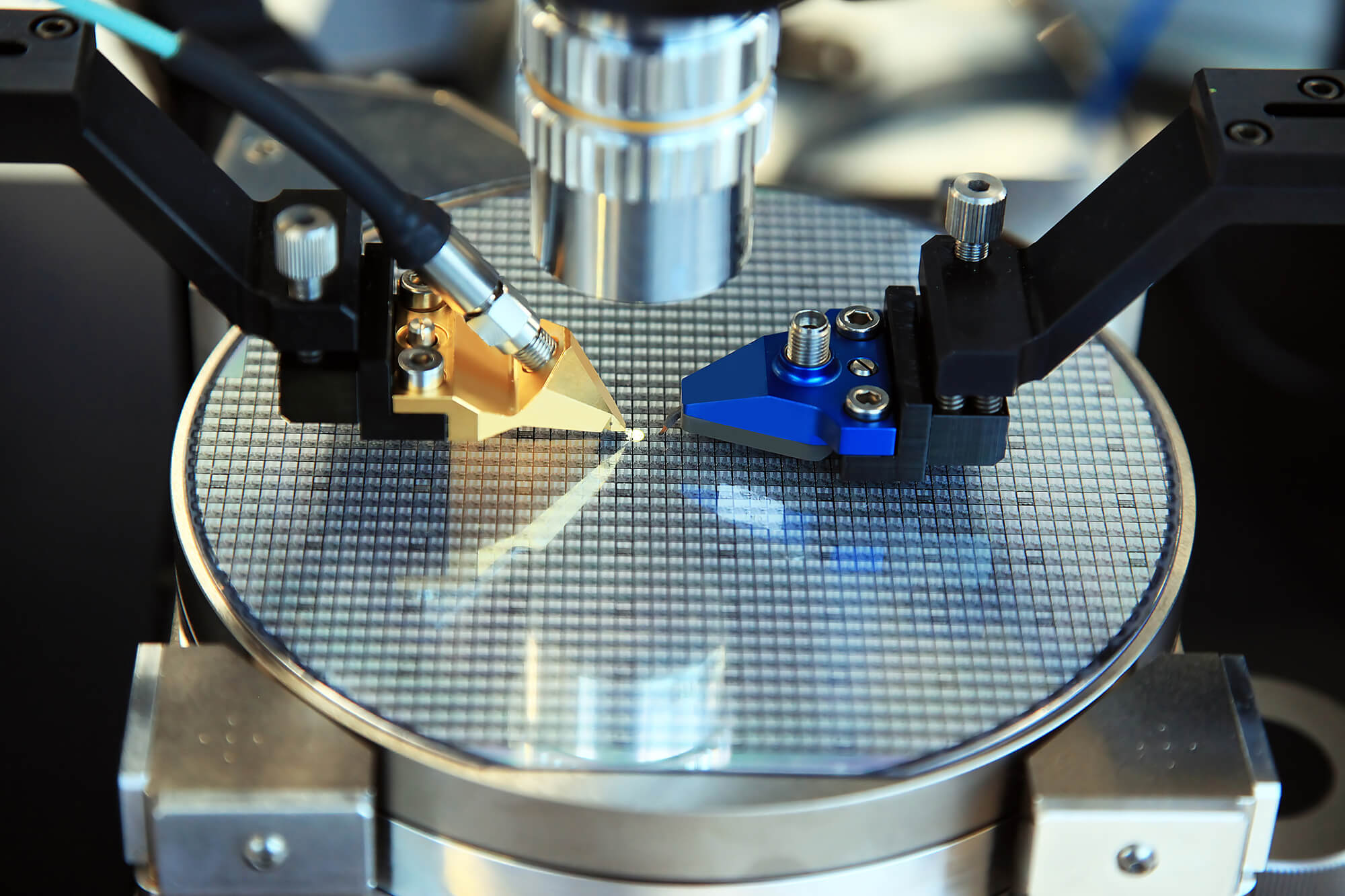 Source: Wafer World
This Substack will focus on the structure of the semi test ecosystem. However, we are seeing a lot of interesting movements in the test market with the recent and ongoing earnings season, so real-time commentary on what’s going on will be included in our end-of-week Weekly Update. Be sure to check it out tomorrow.
Chips’s Substack is a reader-supported publication. To receive new posts and support my work, consider becoming a free or paid subscriber.
Why AI Demands More Testing
At the heart of this shift are two key factors: increased test intensity per device, and a growing number of test steps due to advanced packaging.
1. Test Intensity Is Higher for AI Chips
AI chips - whether they’re GPU’s or custom ASIC’s - are not your average SoC. These devices are typically much larger, have higher transistor counts, and operate under extreme performance and power constraints. In other words, there’s simply more to test, and the cost of failure is higher.
A typical AI chip may go through:
- More test vectors during functional testing, due to the size and complexity of the logic blocks.
- Longer burn-in and stress testing, needed to ensure optimal operability over time
- Higher demands on test accuracy and coverage, as a single undetected defect in a multi-die module could compromise the entire package and create a big loss.
Put differently, AI chips are not just expensive to build - they’re expensive to test. This drives longer test times, higher utilization of test equipment and a broader set of test steps, especially for high-performance or safety-critical applications.
2. Advanced Packaging Adds More Test Steps
The AI era is also ushering in a new wave of heterogeneous integration and advanced packaging. Think chiplets, 2.5D integration (like TSMC’s CoWoS), 3D stacked memory, and complex interposers bringing the chiplets together.
Each of these innovations adds more test steps:
- Known Good Die (KGD) testing at the wafer level (logic and memory) before chiplets are assembled.
- Wafer-level system integration testing to catch early package failures.
- Post-package testing to validate thermal, electrical, and mechanical performance under final system conditions.
Advanced packaging is also driving new requirements in test interface hardware, like high-density probe cards and thermally controlled test sockets. And because many of these packages involve stacked HBM, or large multi-die packages, traditional test infrastructure is being pushed to its limits - requiring innovation (and capital investment) across the test chain.
Value Chain Winners
This shift is creating real, tangible opportunities across the semiconductor test value chain. Here’s a breakdown of the players (non-exhaustive) who are active in this vertical:
ATE Vendors: Teradyne & Advantest
As test intensity increases, chipmakers need more test throughput and higher-performance testers. Companies like TER -4.90%↓ and Advantest - the dominant players in automated test equipment - are already seeing growing demand from AI customers. But more so the Japanese Advantest compared to the American Teradyne, due to better exposure to CoWoS packages.
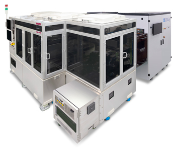 Source: Advantest
However - both companies have noted in recent earnings calls that AI-related test demand is contributing meaningfully to their bookings, particularly in the high-end logic and HBM segments.
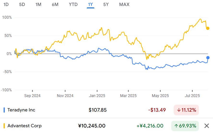 Source: Google Finance
Wafer Probers: Accretech & TEL
Before any AI chip is packaged, it must be tested at the wafer level - and that’s where wafer probers come in. These precision machines align and position wafers between the ATE tool and under the probe cards (discussed later down), enabling electrical contact for the automated test equipment (ATE) to verify each die’s functionality.
As AI drives more wafer-level test (WLT) - the demand for high-performance and reliable probers is rising.
Leading suppliers include:
- Accretech (Tokyo Seimitsu) – a top-tier Japanese firm known for advanced logic and memory probing systems.
Tokyo Electron (TEL) – better known for its front-end fab equipment tools, but also a key provider of high-precision probers for advanced nodes (but an overall niche part of their total business).
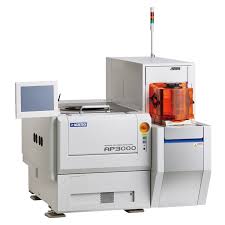
Source: Accretech
What’s changing?
- AI chips often use large-area reticles and high pin-count dies, requiring more precise wafer handling and alignment.
- Wafers must be tested multiple times, both before and after partial assembly (e.g. mid-bond testing in 3DIC).
With test becoming more front-loaded and complex, wafer probers are no longer commodity tools - they are now critical infrastructure for AI chip production. Expect sustained demand as chipmakers prioritize early defect screening and wafer-level testing steps.
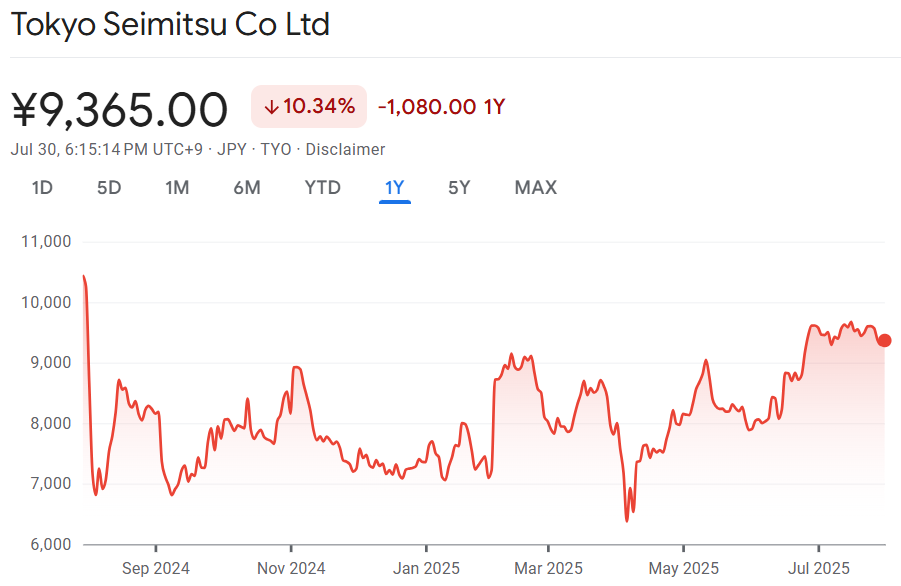 Source: Google Finance
Probe Card Suppliers: Technoprobe, FormFactor & MJC
Advanced packaging and wafer-level testing drive demand for high-performance probe cards - the consumable interface between the prober and the wafer. Probe cards must now accommodate:
- Higher pin counts and tighter pitches.
- Complex test configurations for chiplets and interposers.
- Thermal management features for high-power AI parts.
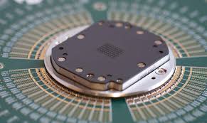 Source: Technoprobe
Technoprobe (Italy), MJC (Japan) and FORM -5.25%↓ (US) are global leaders in this space. Technoprobe recently highlighted AI and high-performance computing (HPC) logic die as key growth areas, while FormFactor & MJC dominate the memory market (with FormFactor supplying to Hynix and MJC supplying Samsung & MU -11.68%↓).
Moreover, each chip design has it’s own unique probe card. They are non-transferrable between chips. So shorter cycle product launches from NVDA 0.23%↑ & AMD -7.57%↓ coupled with an ever-growing number of ASIC’s entering the market are structural tailwinds pushing revenues and growth opportunities for these companies.
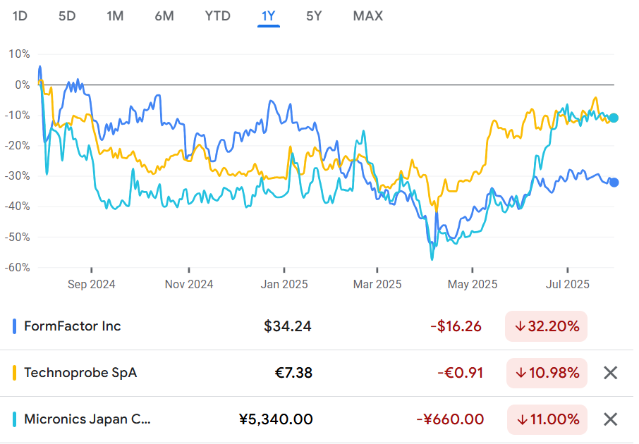 Source: Google Finance
Socket Suppliers: WinWay, Enplas, LEENO & ISC
The components that interface chip packages with testers - such as the test socket - are becoming more specialized. WinWay Technology, a Taiwanese socket supplier, along with Enplas (Japanese), LEENO (Korean) & ISC (Korean) are seeing (at varying levels of exposure) growing orders and revenues from both test houses and system companies working on AI accelerators . Their products must now withstand:
- Higher thermal stress.
- More frequent insertion/removal cycles.
- Lower signal loss at high frequencies.
These requirements are pushing the socket suppliers into a more strategic role, especially as packaging complexity grows.
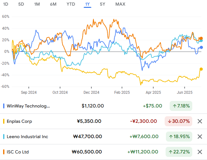 Source: Google Finance
OSAT’s: KYEC, ASE & Amkor
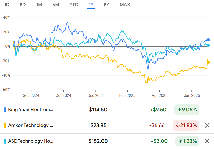
OSAT’s - especially those with a strong focus on testing - are also set to benefit. Despite naming some of the bigger OSAT names, a major beneficiary of the AI ramp has been Taiwanese KYEC (King Yuan Electronics), who essentially has a monopoly on NVDA 0.23%↑ GB package testing as well as exposure to AMZN 2.00%↑’s ASIC’s.
Meanwhile, large players like ASE and AMKR -2.87%↓ are expanding their test-centric packaging services, offering integrated flow from wafer sort through final system-level test (SLT). These services are critical for AI chips that must hit aggressive time-to-market windows while maintaining high yield.
 Source: Google Finance
Burn-In Testing: AEHR & Pentamaster
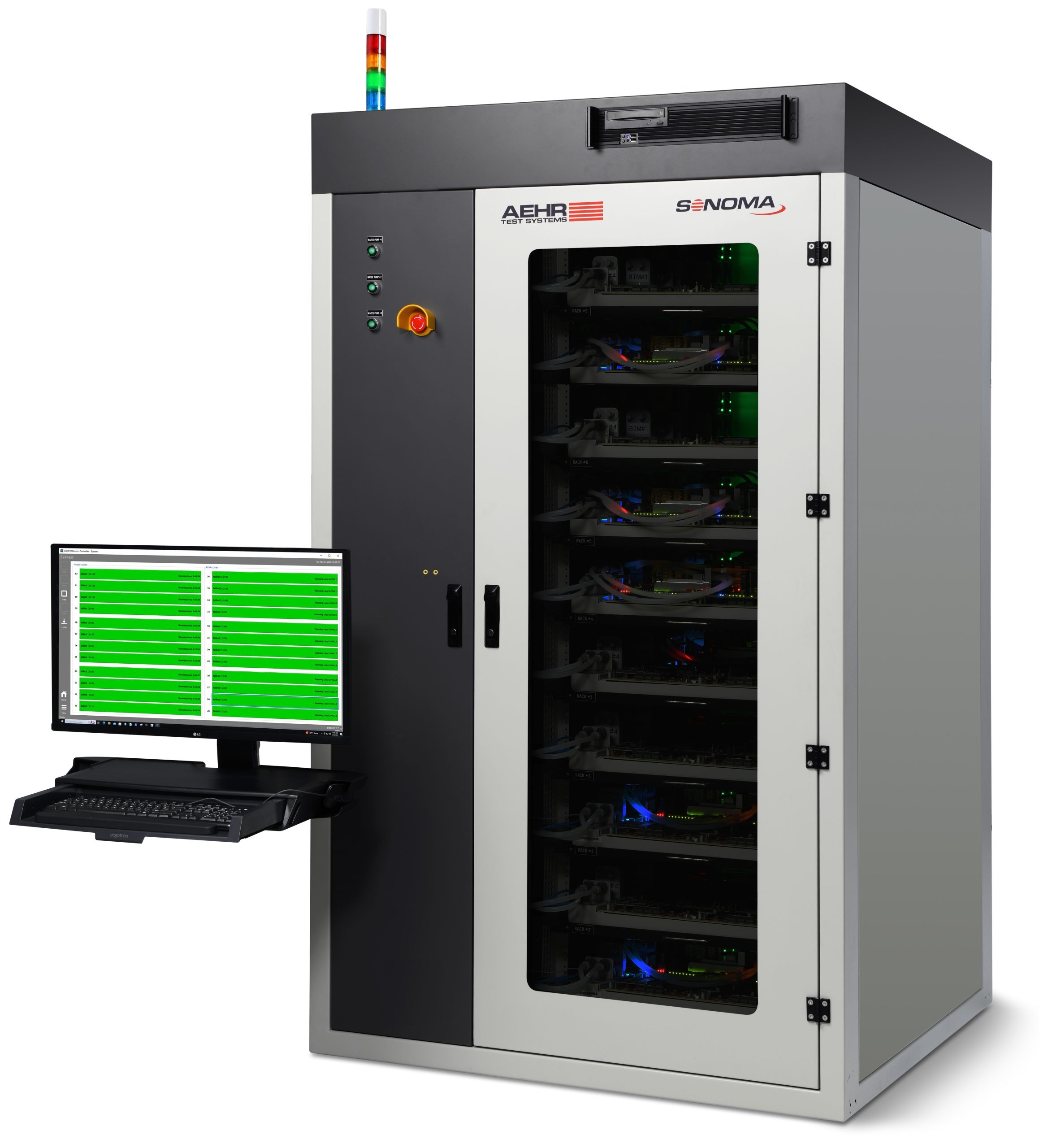
As AI chips grow more complex and power-hungry, burn-in testing is becoming a critical step to catch early-life failures before chips are deployed in data centers. This involves stressing chips under high temperature and voltage to weed out latent defects.
Burn-in saw a huge surge during the Silicon Carbide EV rush when most SiC MOSFET’s were required to undergo burn-in testing to ensure smooth and reliable performance before customers purchased their vehicles and started driving them on the road.
However, since the slowdown of EV penetration and the rise of AI, some Data Center chips are now undergoing burn-in to ensure that once they are depolyed - they will function reliably.
 Source: AEHR
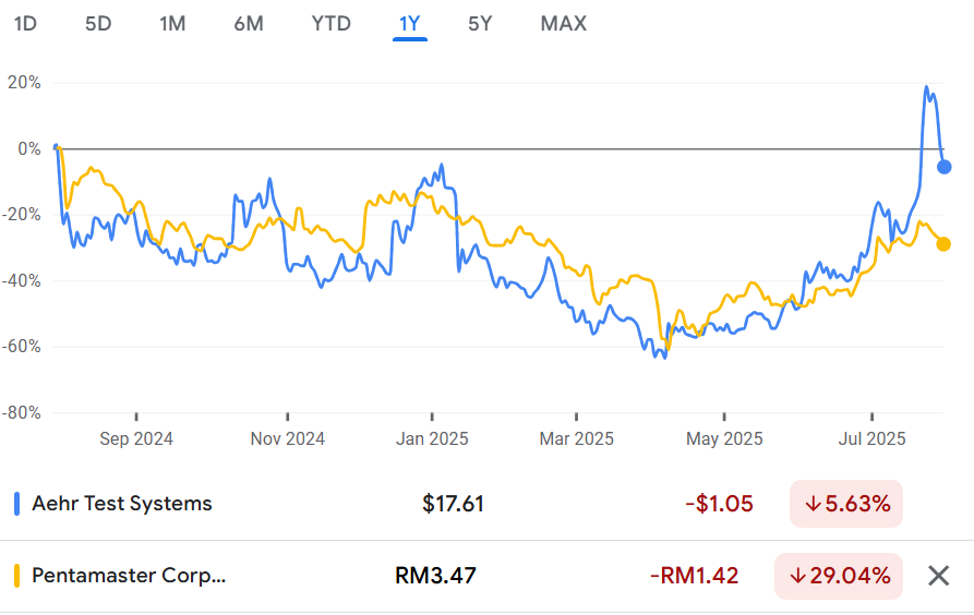
Traditional packaged burn-in is costly and slow, so the industry is shifting toward wafer-level burn-in, which allows testing many dies in parallel before packaging. This is where US-based AEHR -6.15%↓ Test Systems & Malaysian Pentamaster come in.
AEHR & Pentamaster provide wafer-level burn-in and reliability systems, and are seeing rising demand tied to AI & Data Center chips.
In the AI-driven test ecosystem - as packaging costs soar, catching failures earlier is no longer optional - it’s an operational necessity.
 Source: Google Finance
A New Era of Test Economics
The impact of AI on semiconductor test is not just technical - it’s economic. According to industry analysts, test cost as a percentage of total chip cost is rising again after years of decline. In advanced AI packages, it can now account for 10–15% of total cost, compared to ~5% in traditional mobile or consumer SoCs.
This creates both pricing power and volume leverage for test suppliers - an enviable position in an industry often marked by margin pressure.
Final Thoughts
AI is often discussed in terms of GPU multi-gigawatt clusters, datacenter buildouts, or model training - but its ripple effects extend deep into the semiconductor supply chain. As chips grow more complex and packaging more advanced, testing is becoming a chokepoint - and a profit center.
For investors, engineers, and industry watchers alike, the test value chain is no longer an afterthought. It’s a structural beneficiary of the AI wave - quietly but decisively capturing its own share of the AI upside.
Disclosure:
The information provided in this publication is for informational and educational purposes only and should not be construed as investment advice or a recommendation to buy or sell any securities. All opinions expressed are those of the author and are subject to change without notice. The content may contain forward-looking statements that involve risks and uncertainties, and actual results may differ materially.
Before making any investment decisions, you should consult with a qualified financial advisor or other professional who is familiar with your individual financial situation and objectives. Investing involves risk, including the potential loss of principal. Past performance is not indicative of future results.
Chips’s Substack is a reader-supported publication. To receive new posts and support my work, consider becoming a free or paid subscriber.
第二部分:解析(深度解读)
一、这篇文章为什么重要
在 AI 算力军备竞赛的叙述里,市场目光几乎都集中在 GPU、HBM、先进封装(CoWoS)和晶圆代工产能上,而「测试(test)」这个夹在制造与封装之间的环节,长期处于叙事的盲区。本文的价值恰恰在于把这条被忽视的价值链单独拎出来,指出一个反直觉的事实:AI 芯片越是昂贵、复杂,测试环节的成本占比和战略地位就越高。
对工程师和投资者而言,这有两层含义。其一是「卡脖子」视角的转移——当一颗多 die(多芯片)的 AI 加速器里只要有一个 die 存在漏检缺陷,整颗 package 就可能报废,损失被放大到整个封装成本;于是测试从「出厂前的质检」变成「决定良率与毛利的关键工序」。其二是投资视角的转移——测试不再是一个低增速、强周期的「卖铲子」生意,而是在 AI 带动下同时获得「量(volume)」与「价(pricing power)」两端杠杆的结构性受益环节。这一点与本站此前关于 CPO/先进封装测试瓶颈的讨论高度互补(见下方「四、相关文章」)。
二、核心论点拆解
文章主线可以拆成两条驱动因素 + 一条价值链映射 + 一个经济性结论:
| 维度 | 核心论点 | 关键证据/数据 |
|---|---|---|
| 单芯片测试强度(Test Intensity) | AI 芯片更大、晶体管更多、功耗/性能约束更极端 → 可测内容更多、失效代价更高 | 更多测试向量、更长的 burn-in/应力测试、对覆盖率要求更高 |
| 先进封装新增测试步骤 | Chiplet、2.5D(CoWoS)、3D 堆叠 HBM、interposer 每层都需测试 | KGD 晶圆级已知良晶测试、晶圆级系统集成测试、封装后测试 |
| ATE(自动测试设备) | 测试吞吐与性能需求上升,Advantest 因 CoWoS 曝光优于 Teradyne | 两家公司财报电话会均确认 AI 相关测试订单显著贡献 |
| 晶圆探针台 | WLT(晶圆级测试)需求上升,探针台从「商品工具」变为「关键基础设施」 | 大光罩(large-area reticle)、高 pin 数 die、3DIC mid-bond 多次测试 |
| 探针卡 | 高 pin 数/细 pitch/散热需求;每款芯片专用、不可通用 → 强复购 | Technoprobe(逻辑/HPC)、FormFactor(供 Hynix)、MJC(供 Samsung/MU) |
| 测试插座(Socket) | 高散热、高频低损耗、插拔频次提升 → 战略地位上升 | WinWay(台)、Enplas(日)、LEENO/ISC(韩) |
| OSAT | 测试型封测受益,KYEC 近乎垄断 NVDA GB 封装测试 | ASE、Amkor 扩张 test-centric 集成服务(含 SLT 系统级测试) |
| 老化测试(Burn-In) | 数据中心芯片引入 burn-in 以筛除早期失效 | 从 SiC EV 需求转向 AI;晶圆级 burn-in 成趋势(AEHR、Pentamaster) |
| 测试经济学 | 测试成本占芯片总成本从 ~5%(手机/消费 SoC)升至 AI 封装的 10–15% | 同时带来定价权与量的杠杆 |
这张表把原文分散在「Why AI Demands More Testing」与「Value Chain Winners」两节的内容做了统一归位:前两项是需求端的「因」,中间六项是价值链上的「果」,最后一项是落到财务模型上的「果」。
三、关键概念 / 技术解读
1. 测试强度(Test Intensity)与测试向量(Test Vectors) 测试向量是 ATE 施加到芯片输入端、并比对输出响应的激励-期望序列。逻辑块越庞大复杂,覆盖所有功能与故障模型所需的向量数量越多,单颗芯片的功能测试时间随之拉长。文章所谓「longer test times, higher utilization of test equipment」实质上是:同样的 ATE 机台,因单位测试时长上升,等效产能被「吃掉」,从而需要采购更多机台——这正是 ATE 厂商量价齐升的微观机制。
2. 已知良晶(Known Good Die, KGD)与多阶段测试 在 chiplet 架构下,die 在组装前先单独验证为「良晶」,才能进入 2.5D/3D 集成,否则把一颗坏 die 和高价值 HBM、interposer 封在一起,沉没成本极高。因此测试被「前移(front-loaded)」到晶圆级,并在 partial assembly(如 3DIC 的 mid-bond)后再次测试。文章强调 wafer probers「不再是 commodity tools」,指的就是这种多阶段、高精度、在线复测的需求把探针台推到了产线关键路径上。
3. 探针卡(Probe Card)的「专用性」护城河 「each chip design has its’s own unique probe card… non-transferrable」是全文最值得投资者记住的一句话。探针卡是 prober 与 wafer 之间的消耗性接口,随每款芯片的 pin 图、pitch、电源/地分布而定制。NVDA、AMD 加速迭代 + 大量 ASIC 涌入,意味着探针卡不仅是耗材,更是「设计绑定型复购」——产品生命周期越短、SKU 越多,探针卡厂商的营收可见度反而越高。这是 Technoprobe/FormFactor/MJC 区别于传统周期股的本质。
4. 封装后测试与系统级测试(SLT, System-Level Test) 文章提到 ASE/Amkor 提供「从 wafer sort 到 final system-level test」的集成流。SLT 在接近真实系统工况(电源、散热、高速 SerDes 负载)下验证整 package,是 AI 芯片在激进上市窗口下守住良率的最后一道闸。SLT 设备与高频 socket 正是 WinWay、Enplas 等插座厂的价值放大点。
5. 晶圆级老化(Wafer-Level Burn-In, WLTBI) 传统封装后 burn-in 慢且贵;晶圆级 burn-in 在封装前并行筛除早期失效 die,直接降低封装沉没成本。这正是 AEHR(美)与 Pentamaster(马来)在 AI 数据中心芯片上的增量逻辑——之前其需求主要来自 SiC EV 功率器件,如今切换到更大、更贵的 AI 市场。
四、与本站其他 CPO / 硅光系列文章的链接
- CPO 最大的瓶颈:高产量测试(High-Volume Testing):本文与这篇互补性最强——那篇从 CPO/光互连量产角度谈「测试是放量瓶颈」,本篇则从整个 AI 半导体测试价值链给出更宏观的框架。
- TSMC 在 CPO 领先,三星第三颗芯片:本文多次点名的 CoWoS 正是 TSMC 先进封装的核心,也是 Advantest 相对 Teradyne 更具曝光优势的根源,可对照阅读。
- CPO 的幻象(CPO 专题终章):从更宏观的 CPO 落地节奏与产业现实切入,帮助理解为什么测试/封装这类「苦活」会成为 AI 算力扩张中确定性更高的受益环节。
五、投资意义
文章覆盖了一条相当完整的「测试价值链」标的清单,按环节归纳如下(均依原文提及):
- ATE(整机): Advantest(日,受惠 CoWoS 曝光更强)、Teradyne(TER,美)。
- 晶圆探针台: Accretech/东京精密(日)、Tokyo Electron(TEL,前端设备为主、探针台为其利基)。
- 探针卡: Technoprobe(意,逻辑/HPC)、FormFactor(FORM,美,内存/Hynix)、MJC(日,Samsung/MU)。
- 测试插座: WinWay(台)、Enplas(日)、LEENO(韩)、ISC(韩)。
- OSAT(测试型封测): KYEC/京元电子(台,近乎垄断 NVDA GB 封装测试 + AMZN ASIC)、ASE(日月光)、Amkor(AMKR)。
- 老化测试: AEHR Test Systems(美)、Pentamaster(马来)。
- 下游拉动方: NVDA、AMD、AMZN(ASIC)、MU(美光)、Hynix、Samsung(HBM/内存)。
投资含义可提炼为三层:(1)确定性排序——离「每颗芯片必测、且随迭代加速复购」最近的环节(探针卡、OSAT 测试、ATE)确定性最高;(2)地域错位——Advantest 因 CoWoS 曝光优于 Teradyne,提示同样的 AI 主题在不同公司上的弹性差异;(3)隐性期权——晶圆级 burn-in(AEHR、Pentamaster)是从 SiC EV 需求放缓后切换到更大 AI 市场的第二增长曲线。对关注本站的读者,这条链与 CPO/硅光放量所依赖的「高产量测试能力」是同一底层约束,值得作为 AI 算力外溢的「铲子」组合一并跟踪。
六、风险提示
- 周期属性未被消除: 测试设备资本开支仍与晶圆厂/封测厂 capex 节奏高度相关,若 AI 服务器需求或 HBM/CoWoS 产能扩张不及预期,ATE 与探针台订单可能回调。
- 集中度风险: 文中多处依赖单一大客户(如 KYEC 对 NVDA GB 封装测试近乎垄断),客户自测能力(in-house test)扩张或订单转移会直接冲击相关标的。
- 先进封装路线不确定性: 若 chiplet/2.5D 渗透率或技术路线变化,探针卡「每款专用」的复购逻辑与具体 pin/pitch 需求可能随之改变。
- 估值已反映预期: 文章写作时(2025-07)多家标的已随 AI 叙事上涨(文中嵌入的股价快照显示 TER/FORM/AMKR/AEHR 当日均为下跌),需警惕「好逻辑、贵价格」。
- 本文为信息整理,非投资建议: 原作者文末已声明仅供参考、不构成买卖建议;本解读亦同,请以原文及正式财报/招股书为准。
以上解读基于原文信息整理,不构成投资建议。