Co-Packaged Optics (CPO) Book – Scaling with Light for the Next Wave of Interconnect — 共封装光学(CPO)与 Book 式扩展
SemiAnalysis 重磅 CPO 专题(英文原文 + 中文深度解读):从 TCO/功耗、SerDes 瓶颈、TSMC COUPE、MZM/MRM/EAM 调制器到 NVIDIA 与 Broadcom 的 CPO 供应链,系统拆解共封装光学如何驱动下一代互联扩展。
本文整理自 SemiAnalysis(Substack)(https://semianalysis.com),原文发布于 Jan 02, 2026(标题原文:Co-Packaged Optics (CPO) Book – Scaling with Light for the Next Wave of Interconnect)。 结构为 正文(英文原文)+ 解析(中文深度解读),方便中英对照阅读。 来源说明:内容经公开页面获取;本发布保留完整英文原文并附中文深度解读,仅作信息整理与学习用途,著作权归原作者所有,建议在原站支持作者订阅。 ⚠️ 本文含付费段落,以下仅发布公开可读部分;付费深解未包含。
第一部分:正文(Original Article)
Co-Packaged Optics (CPO) Book – Scaling with Light for the Next Wave of Interconnect
Scale-out and Scale-up CPO, CPO TCO and Power Budgets, DSP Transceivers vs LPO vs NPO vs CPO, TSMC COUPE, MZM vs MRM vs EAM Modulator Deep Dive, CPO Focused companies and CPO Supply Chain
Dylan Patel, Daniel Nishball, Myron Xie, and 3 others
Co-Packaged Optics (CPO) has long promised to transform datacenter connectivity, but it has taken a long time for the technology to come to market, with tangible deployment-ready products only arriving in 2025. In the meantime, pluggable transceivers have kept pace with networking requirements and remain the default path thanks to their relative cost-effectiveness, familiarity in deployment, and standards-based interoperability.
However the heavy networking demands that come with AI workloads mean that this time is different. The AI networking bandwidth roadmap is such that interconnect speed, range, density and reliability requirements, will soon outpace what transceivers can provide. CPO will provide some benefit and bring more options to scale-out networking, but it will be central to scale-up networking. CPO will be the main driver of bandwidth increases in scale-up networking for the latter part of this decade and beyond.
Today’s copper-based scale-up solutions, such as NVLink, provide tremendous bandwidth of 7.2 Tbit/s per GPU – soon to be 14.4 Tbit/s per GPU in the Rubin generation, yet copper-based links are limited in range to two meters at most, meaning the scale-up domain world size is limited to one or two racks at most. It is also increasingly difficult to scale bandwidth over copper. In Rubin, Nvidia will deliver another doubling of bandwidth per copper lane through bi-directional SerDes, but doubling bandwidth on copper by developing ever-faster SerDes is a highly challenging vector of scaling that is a slow grind. CPO can deliver the same or better bandwidth density and can provide additional vectors for scaling bandwidth, all while enabling larger scale-up domains.
A starting point for understanding the impetus for CPO is to consider the many inefficiencies and trade-offs when using a transceiver for optical communication. Transceivers can be used to achieve greater link range, but the cage on the front panel of a networking switch or compute tray that transceivers plug into is typically situated 15-30cm from an XPU or switch ASIC. This means that signals must first be transmitted electrically using an LR SerDes over that 15-30cm distance, with the electrical signal recovered and conditioned by a Digital Signal Processor (DSP) within the transceiver before being converted into an optical signal. With CPO, optical engines are instead placed next to XPUs or Switch ASICs, meaning that the DSP can be eliminated and that lower power SerDes can be used to move data from the XPU to the Optical Engine. This can reduce energy required to transmit data by more than 50% when compared to DSP Transceivers - with many aspiring to reduce energy requirements per bit by as much as 80%.
 Source: SemiAnalysis
While scale-out CPO solutions like Nvidia and Broadcom’s are garnering more attention and are being closely looked at by end customers, major Hyperscalers are already starting to plan out their scale-up CPO strategy and are committing to suppliers. For instance, Celestial AI is estimating that they could generate a $1B revenue run rate by the end of calendar year 2028 - we believe this will primarily be driven by a CPO scale-up solution shipping with Amazon’s Trainium 4.
CPO focused companies are now well beyond papers, pilot projects and demonstrations and and are making key product decisions such as optical port architecture to solve for high volume manufacturing. CPO for scale-up is now not a matter of if and why, but when and how – how to bring these systems to volume production, and when key component supply chain companies like laser manufacturers can ramp up sufficient production.
This article will present an in-depth discussion on the benefits and challenges of CPO, how CPO architectures work, current and future CPO products, CPO focused companies, CPO-related components and their respective supply chains. This piece is intended to serve as a guide to practitioners, industry analysts, investors and everyone else who is interested in interconnect technology.
Table of Contents and Guide to this Article
We have segmented the article into five parts – readers are welcome to focus on sections that are most interesting or relevant to them.
In Part 1: CPO Total Cost of Ownership (TCO) Analysis, we start off by analyzing how adoption of CPO changes the total cost of ownership for scale-out and scale-up networks. We think that TCO, reliability, and equipment vendor bargaining power will be the primary considerations for adopting CPO in scale-out networks. We will explore whether CPO is ready for primetime when it comes to scale-out, touching on the data we have so far on solution reliability such as Meta’s CPO scale-out switch study presented at ECOC 2025.
In Part 2: CPO Introduction and Implementation, we will dive deeper into how CPO works. This section will explore the evolution of the market from copper to co-packaged copper and from digital signal processor (DSP) optics to linear pluggable optics (LPO) to CPO and the impetus and arguments for the adoption of CPO. SerDes scaling limits and Wide I/O as an alternative to SerDes – particularly when used in conjunction with CPO – will also be discussed.
In Part 3: Bringing CPO to Market, we will describe critical technologies that will enable CPO to gain traction and come to market. We first discuss Host and Optical Engine packaging and explain TSMC COUPE in detail and why it is emerging as the integration option of choice. Fiber Attach Units (FAUs), Fiber coupling as well as Edge Coupling vs Grating Couplers will be explained thoroughly. We will cover modulator types such as Mach-Zender Modulators (MZMs), Micro-Ring Modulators (MRMs) and Electro-Absorption Modulators (EAMs). This section will end with explaining the core of why CPO is being adopted – the many different vectors for scaling bandwidth with CPO: More fibers attached, using wavelength division multiplexing (WDM) and higher order modulation.
In Part 4: CPO Products of Today and Tomorrow, we will analyze CPO products available on the market today and their associated supply chain. We will start with Nvidia and Broadcom’s solutions before discussing major CPO companies. We cover Ayar Labs, Nubis, Celestial AI, Lightmatter, Xscape Photonics, Ranovus and Scintil, describing each provider’s solution in detail and weigh in on important puts and takes for each company’s approach.
Finally, in Part 5: Nvidia’s CPO Supply Chain, we will conclude this report by describing in detail the supply chain for Nvidia’s CPO ecosystem, naming key suppliers for Laser Sources, ELS Modules, FAU, FAU Alight Tools, FAU Assembly, Shuffle Box, MPO Connectors, MT Ferrules, Fibers, and E/O Testing.
Part 1: CPO Total Cost of Ownership (TCO) Analysis
One of the most highly anticipated topics at Nvidia’s GTC 2025 earlier this year was Jensen announcing the company’s first CPO-enabled scale out network switches. Notably, for scale-up, Nvidia is still pushing forward with copper and going to extreme lengths to avoid going to optics, even out to 2027 and 2028.
Let’s begin our discussion regarding these new CPO-enabled switches by examining their total cost of ownership, analyzing the cost and power savings for scale-out CPO can deliver.
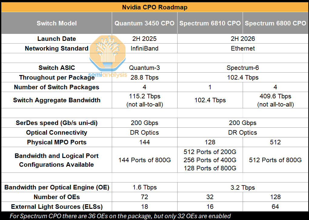
Nvidia’s GTC 2025 keynote announced three different CPO scale-out switches that utilize two different CPO-enabled switch ASICs. While there are TCO, power, and deployment speed benefits – they are not compelling enough for customers to jump headfirst into an entirely different deployment regime, and we expect to see limited adoption for the first wave of CPO scale-out switches. Let’s go through why.
 Source: SemiAnalysis
Typical AI Cluster Networking Configuration and TCO
A typical AI Cluster has three main networking fabrics, back-end, front-end and out of band management fabric. The most heavily utilized and technically demanding network fabric is the back-end fabric. The back-end fabric is used for scale-out communications between GPUs to communicate with one another and exchange data in collective operations to parallelize training and inference. Back-end networks typically use the InfiniBand or Ethernet protocols.
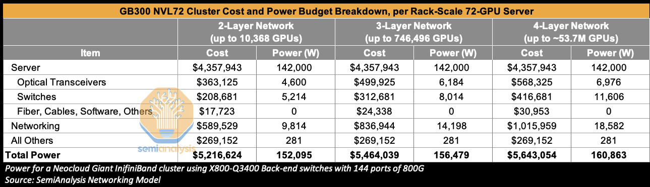
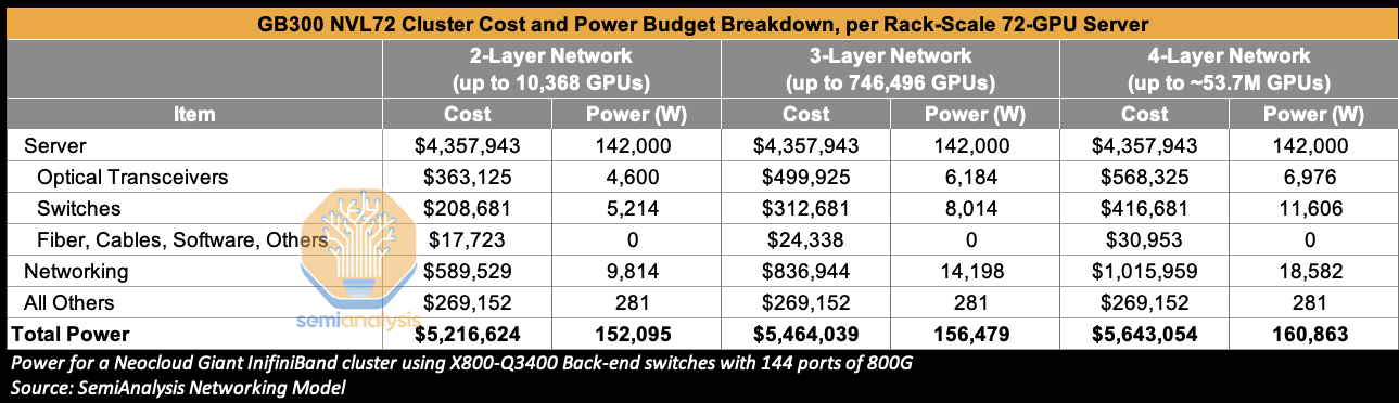
Because of its demanding nature, the back-end network accounts for a dominant share of total networking cost and power, representing 85% of networking cost and 86% of networking power for 3-layer GB300 NVL72 clusters deployed on InfiniBand using Nvidia’s X800-Q3400 back-end switches. CPO-based switches and networking solutions can be used in both the back-end and front-end network, but we think that the focus for deployment at this stage will be in the back-end network. Readers can find much more details on back-end network topology, port, switch, and transceiver counts in our Optical Boogeyman Article from 2024 as well as in our AI Networking Model. Those that would like to understand total networking cost of ownership can read our AI Neocloud Anatomy and Playbook article.
Zooming out – networking cost is the second largest component of total AI cluster cost behind the AI server itself. In a GB300 NVL72 Cluster with a 3-Layer InfiniBand network, this stands at 15% of total cluster cost, reaching 18% of total cluster cost for a 4-Layer network. Optical transceivers are a significant portion of this cost, accounting for 60% of networking cost for a 3-Layer network when using the relatively more expensive Nvidia LinkX Transceivers. They also consume 45% of total networking power for a 3-Layer network.
 Source: SemiAnalysis AI Networking Model
The greater the number of GPUs in an AI cluster, the more likely it is that more networking layers will be needed. Going from a two-layer to a three-layer network and beyond means higher costs and a greater power budget. CPO can both help reduce power and cost holding number of layers constant, and can reduce total power and cost requirements by expanding the number of GPUs that can be connected on a network of a given number of layers.
CPO Scale-out Power Budgets
Earlier this year, at GTC 2025, Nvidia’s CEO Jensen Huang highlighted the immense power consumption from transceivers alone as a key impetus for CPO. Using some of the per-rack power budgets from the above table, a 200,000 GB300 NVL72 (72 GPU packages and 144 compute chiplets per rack) GPU cluster on a three-layer network would consume 435 MW of Critical IT Power of which 17 MW would be consumed by optical transceivers alone. Clearly there is an immense amount of power that can be saved by eliminating most of the transceiver content.
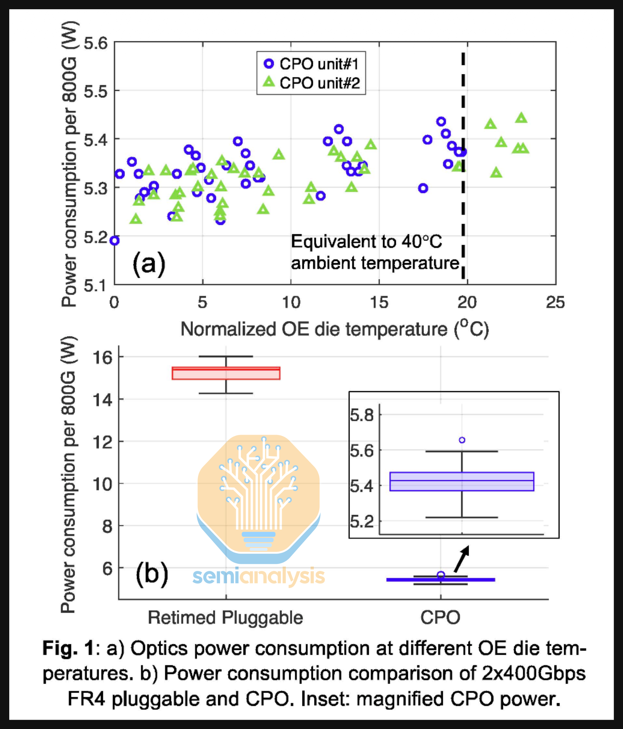
This can be easily seen by comparing the power used in just one 800G DSP transceiver to the power consumed by optical engines and laser sources (per 800G bandwidth) within a CPO system. While an 800G DR4 optical transceiver consumes about 16-17W, we estimate that the optical engine together with external laser sources used in Nvidia’s Q3450 CPO switch consume about 4-5W per 800G of bandwidth, a 73% reduction in power.
These figures are very close to those presented by Meta in its paper published and presented at ECOC 2025. In this report – Meta showed how an 800G 2xFR4 pluggable transceiver consumes about 15W while the optical engine and laser source within the Broadcom Bailly 51.2T CPO switch consumes about 5.4W per 800G of bandwidth delivered, a 65% power savings.
 Source: Meta
Let’s expand this analysis to the cluster level. Turning to a GB300 NVL72 cluster built on a three-Layer network, we see that moving from DSP transceivers to using LPO transceivers in the back-end network can reduce total transceiver power by 36% and total network power by 16%. A full transition to CPO yields even greater savings vs DSP optics – cutting transceiver power by 84% – though part of this power saving is offset by adding optical engines (OEs) and external light sources (ELSs) to the switches, which now consume 23% more power in aggregate. In the below example, optical transceiver power in the CPO scenario remains floored at 1,000W per sever because we assume that front-end networking will still use DSP transceivers.
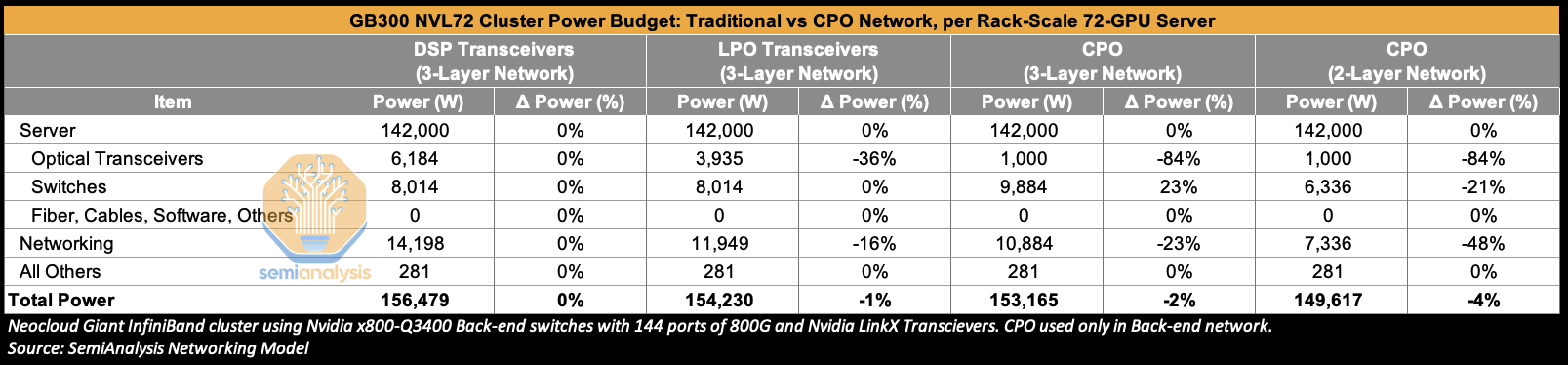 Source: SemiAnalysis AI Networking Model
The use of Nvidia’s CPO scale-out switches implicitly means a high radix network is used by default, though this is “abstracted” from the end users because the shuffle happens inside the switch box as opposed to outside the switch box via patch panels or octopus cables when using high radix non-CPO switches. Instead, these Nvidia CPO switches present themselves as having a very high port count – the Quantum 3450 offering 144 ports of 800G, and the Spectrum 6800 offering 512 ports of 800G for example. We use the word “by default” because Nvidia’s non-CPO InfiniBand Quantum Q3400 switch also offers 144 ports of 800G, though its other InfiniBand switches such as the QM9700 only offer 32 ports of 800G - with only the former offering this “high radix in a box” to deliver a high number of effective ports. This high port count could potentially allow customers to flatten a network from a three-Layer to a two-layer network and is also saves customers the trouble of deploying shuffle boxes and patch panels or unwieldy octopus cables and could be a key selling point. In the two-layer case, transceiver power is reduced by 84%, switch power is down by 21% and total networking power can be reduced by 48% vs traditional DSP transceivers.
The Spectrum 6800 switch, with its large number of ports in both available logical configurations - 512 ports of 800G – specifically enables this when compared to the Spectrum 6810, which offers 128 ports of 800G, 256 ports of 400G or 512 ports of 200G. For the 128 ports of 800G option using the Spectrum 6810, a network could connect up to 8,192 GPUs for a two-layer network, while the Spectrum 6800 at 512 ports of 800G can connect 131,072 GPUs.
As a brief aside, the maximum number of hosts that can be supported using a switch of k ports on an L-layer network is given by:
2(k²)^(L/2) = (512²)²
The magic comes from the fact that the number of ports k is exponentiated by the number of layers. Thus, for a two-layer network, doubling the number of logical ports by assigning half the bandwidth per port (i.e. slicing an 800G port into two 400G ports) using either an internal shuffle (as is the case with the Spectrum 6800), breakout cables or twin-port transceivers means four times the hosts supported!
The power savings discussed in this section so far, 23% for a three-layer CPO network and 48% going down to a two-layer CPO network sounds fantastic, but the wrinkle is that networking is just 9% of total cluster power to begin with for a three-layer network. So, at the end of the day the impact of switching to CPO is diluted considerably at least for scale-out networks. Switching to use CPO for a three-layer network lowers networking power by 23% but only delivers 2% total cluster power savings. Moving to a two-layer network delivers 48% lower networking cost, but only 4% total cluster power savings.
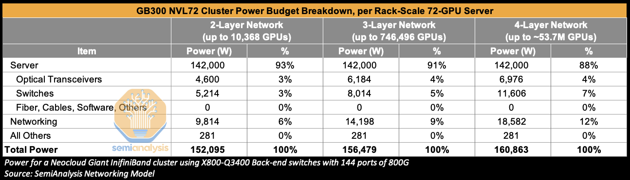 Source: SemiAnalysis AI Networking Model
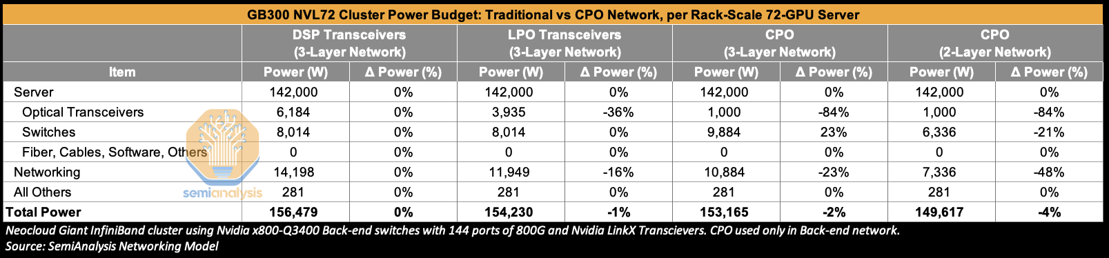 Source: SemiAnalysis AI Networking Model
It is a similar story when looking at total cluster capital cost.
CPO Scale-out Total Cost of Ownership (TCO)
Let’s briefly zoom into some of the cost details when comparing transceivers to a CPO solution. The first Nvidia CPO Switch, the Quantum X800-Q3450 CPO will use 72 optical engines each operating at 1.6Tbit/s; later versions of Quantum CPO switches will likely transition to 36 optical engines at 3.2Tbit/s each, costing ~$1,000 per unit (including FAUs), which translate to $36k of total OE cost per system.
To put this into perspective, consider the total cost if traditional optical transceiver modules were used instead. The non-CPO X800-Q3400 features 72 OSFP cages, and a 1.6T twin-port transceiver is used to provide 144 ports at 800G. Assuming a cost of $1,000 for a generic 1.6T DR8 transceiver, total transceiver cost to populate this switch would amount $72,000, which is double the estimated $35-40k cost of optical engines and ELS needed to deliver the same amount of bandwidth for CPO switch. However, this doesn’t take into account the switch vendor’s margin. If we were to apply a 60% gross margin, optical engine cost to the end buyer would end up at $80k-$90k USD – which is higher cost than the transceiver equivalent. There are still other components like fiber shuffles and other components that would be subject to such a margin stack. This explains why, depending on the cost paid for transceivers and the margin taken by the switch vendor, cost savings when moving to CPO may not be dramatic.
We can see in the table below, when switching from transceivers to CPO on a three-layer network, the additional margin taken on CPO components increases switch costs by 81% which detracts from the 86% savings by not purchasing transceivers. Total networking cost is still 31% lower for CPO than for using DSP transceivers, but as was the case with power, the server rack’s dominant share of cluster TCO means that total cluster costs only drop by 3%.
Flattening the network down to two-layers instead of three-layers can deliver more cost savings though – up to an 7% total cluster cost reduction, with transceiver cost down 86%, and total networking cost decreased by 46%.
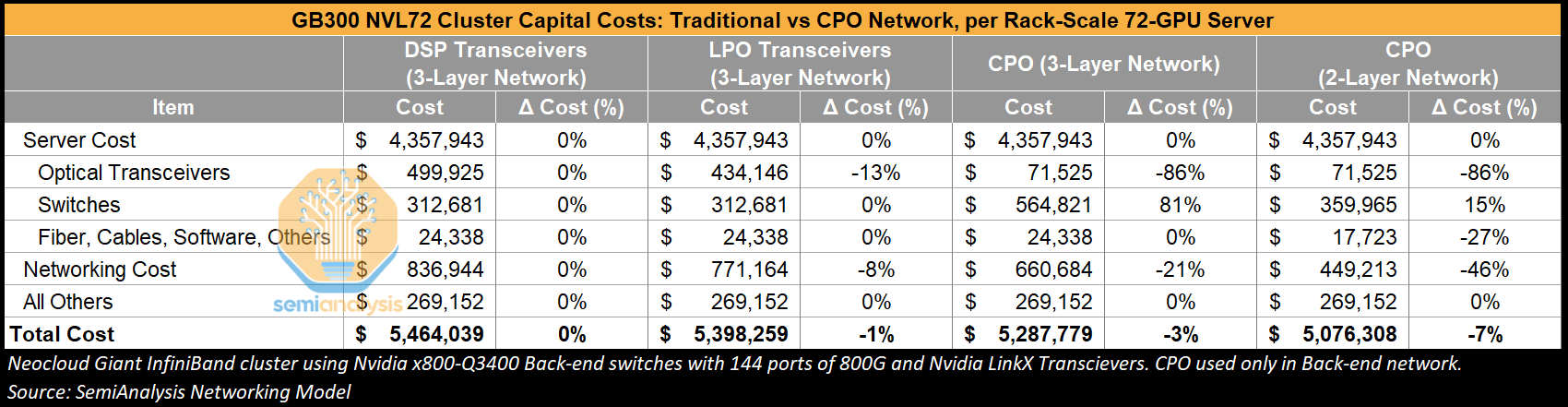 Source: SemiAnalysis AI Networking Model
So – if CPO offers only up to 7% cost savings and up to 4% power savings on one hand, but on the other hand raises concerns about difficult field servicing, anxiety (justified or not) over reliability and blast radius, and the loss of bargaining power that one has with multiple transceiver vendors – why is it being adopted by GPU clouds? The simple answer is that it is not being adopted widely just yet – we do not expect a rapid adoption curve for scale-out CPO systems within hyperscalers in the near term.
CPO for Scale-up Networks
On the contrary, we see CPO for scale-up as the killer application. As mentioned earlier, major hyperscalers are already making commitments to suppliers for deployment of CPO-based scale-up solutions by the end of the decade.
Currently, the incumbent copper-based scale up paradigm is being pushed to its limits due to the limited reach of copper cables – two meters at best when running at 200Gbit/s per lane, as well as the increasing difficulty of doubling bandwidth per lane. CPO can solve these problems as it can meet bandwidth density requirements, provide multiple vectors for scaling bandwidth well into the future as well as unlock much larger scale up world sizes.
Once CPO is deployed for scale-up networking, the scale-up domain will no longer be limited by the interconnect reach. In principle, customers would be able to grow scale-up domains to arbitrarily large sizes. Of course, if one wants to keep the scale-up domain within a single-tier fan-out network that allows for all-to-all connections, the scale-up domain size would become limited by the switch radix.
Scale-out vs Scale-up TAM
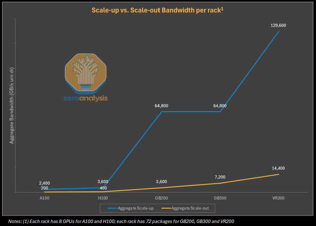
Networking requirements of the scale up fabric are far more demanding than that of the back-end scale-out network. The GPU to GPU or switch links require much higher bandwidth and lower latency to enable the GPUs to be interconnected so that they can coherently share resources such as memory.
To illustrate, 5th generation NVLink on Nvidia Blackwell offers 900GByte/s (7,200 Gbit/s) of uni-directional bandwidth per GPU. That is 9x more bandwidth per GPU than the 100GByte/s (800Gbit/s) per GPU on the back-end scale out network (using the CX-8 NIC for the GB300 NVL72). This also creates the need for much higher shoreline bandwidth density from the host which has been the impetus for pushing GPU SerDes line speeds forward.
It is also important to realize that as the size of scale-up domains increases and as the speed of scale-up interconnect grows as well, the TAM of scale-up interconnect (and eventually, scale-up CPO) has already considerably dwarfed that of scale-out networking. CPO TAM is likely to be dominated by scale-up rather than scale-out networking applications.
 Source: SemiAnalysis
Copper vs Optics for Scale-Up: World Sizes, Density and Reach
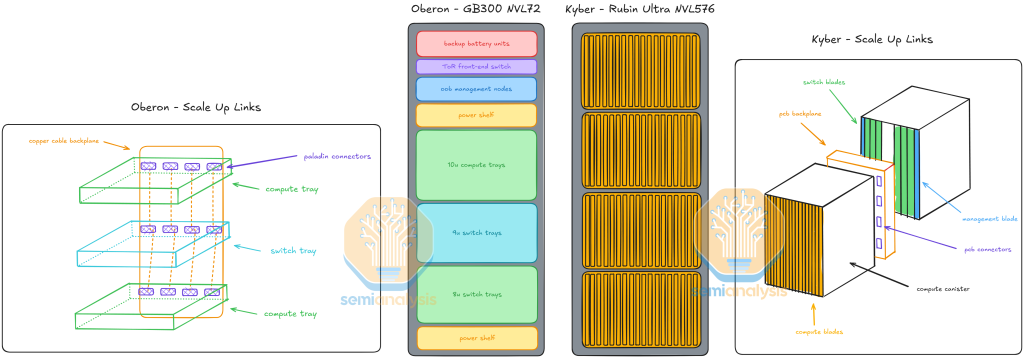
Currently, scale up networks run entirely on copper for good reasons. Matching NVLink bandwidth with optical transceivers in the current pluggable paradigm would be prohibitively expensive in terms of cost and power as well as introducing unwanted latency. There also might not be sufficient face-plate space on the compute tray to even fit all of these transceivers. Copper excels at these low-latency, high-throughput connections. However, as mentioned above, copper’s limited reach restricts the “world size”—the number of GPUs that can be connected within a single scale-up domain.
Increasing scale-up world size is a vitally important avenue of compute scaling. Adding more compute, memory capacity, and memory bandwidth in a single scale up domain has become increasingly critical in today’s regime of inference-based model scaling and test time compute.
Nvidia’s GB200 system offered an immense performance boost because it brought the world size to 72 interconnected GPUs in an all-to-all topology from just 8 interconnected GPUs. The result was unlocking tremendous throughput gains through implementing more sophisticated collective communication techniques that are not feasible on the scale out network.
On copper, this could only be done within the footprint of a single rack creating immense demands on power delivery, thermal management and manufacturability. The complexity of this system has the downstream supply chain still struggling to ramp up capacity.
Nvidia will continue to persist with copper. They also need to push their scale up world size even higher to keep ahead of competitors such as AMD and the hyperscalers who are catching up with their own scale up networks. As such, Nvidia is forced to go to drastic lengths to expand the scale up domain within a single rack. Nvidia’s extreme Kyber rack architecture for Rubin Ultra that was shown at GTC 2025 can scale up to 144 GPU packages (576 GPU dies). This rack is 4x denser than the already dense GB200/300 NVL72 rack. With the GB200 already being so complicated to manufacture and deploy, Kyber takes it to the next level.
Optics enables the opposite approach, scaling across multiple racks to increase world size, rather than packing more accelerators in a dense footprint which is challenging for power delivery and thermal density. This is possible with pluggable transceivers today, but again the costs of optical transceivers along with their high power consumption makes this impractical.
 Source: SemiAnalysis
Copper vs Optics for Scale-Up: Scaling Bandwidth
Scaling bandwidth on copper is also increasingly difficult. With Rubin, Nvidia is achieving the doubling of bandwidth by implementing a novel bi-directional SerDes technology, where both transmit and receive operations share the same channel, enabling full-duplex communication at 224Gbit/s transmit + 224Gbit/s receive per channel. Achieving “true” 448G per lane on copper remains another challenging feat with an uncertain time to market. In contrast, CPO presents multiple vectors for scaling bandwidth: Baud rate, DWDM, Additional Fiber Pairs and Modulation – all of which will be discussed in detail later in this article.
When will CPO be ready for Primetime?
So, if CPO is the solution, why is Nvidia not pursuing it for Rubin Ultra and only for their scale out switches at first? This goes back to supply chain immaturity, manufacturing challenges, and customer hesitation around deployment. The Quantum and Spectrum CPO switches have been introduced to help ramp up the supply chain and get more real world data on reliability and serviceability in the datacenter.
In the interim, Meta’s CPO reliability data published around ECOC provides some helpful information. Meta collaborated with Broadcom for this study, with Broadcom publishing some useful slides as well. In this study, Meta carried out a reasonably sized test run spanning up to 1,049k 400G port device hours across 15 Bailly 51.2T CPO Switches and published the maximum non-zero KP4 forward error correction (FEC) bin:
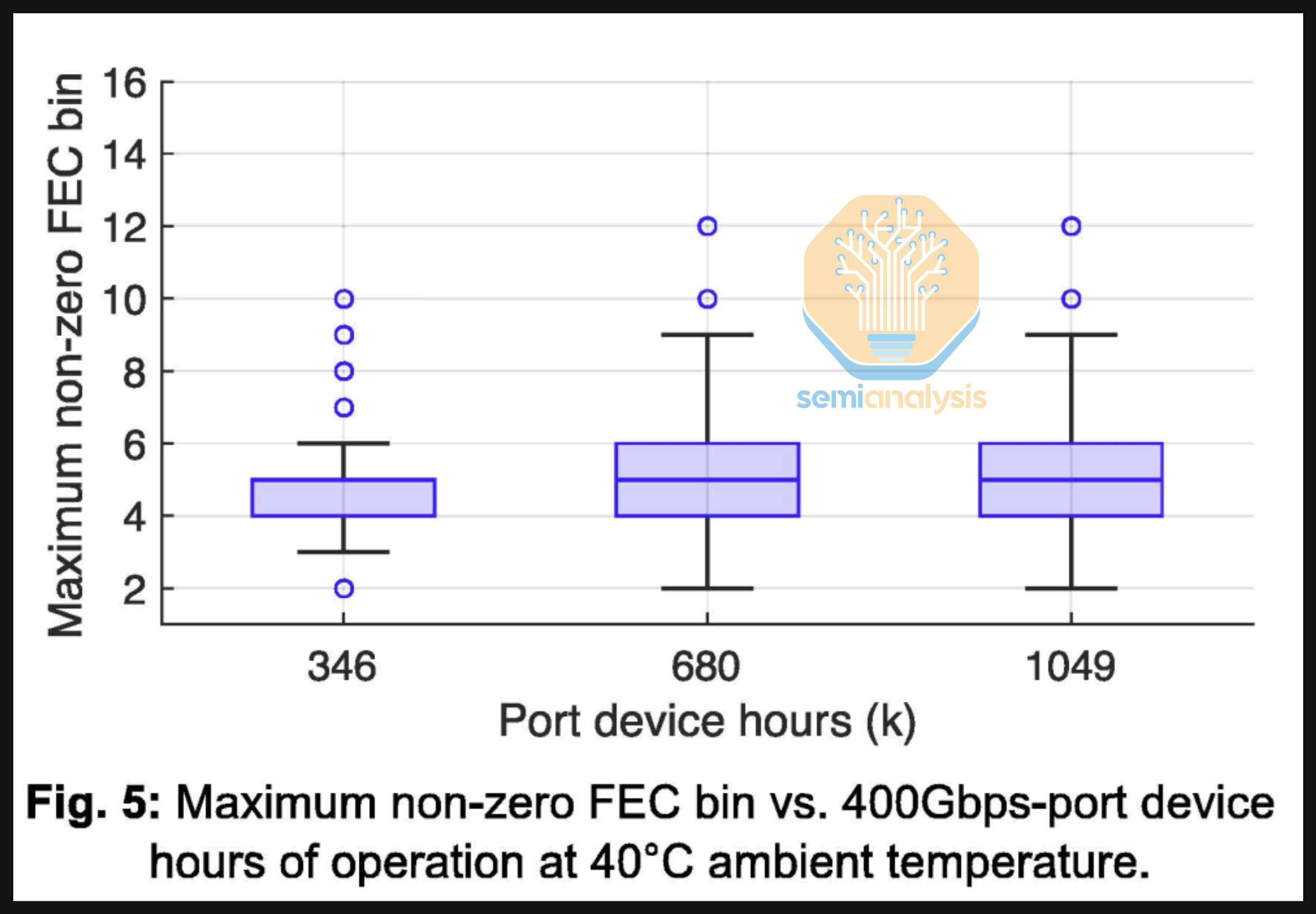 Source: Meta
The paper also explained how during the test period, there were no failures or uncorrectable codewords (UCWs) observed in the links, citing only one instance of FEC bin > 10 being observed across the entire testing period up to 1,049k 400G port device hours.
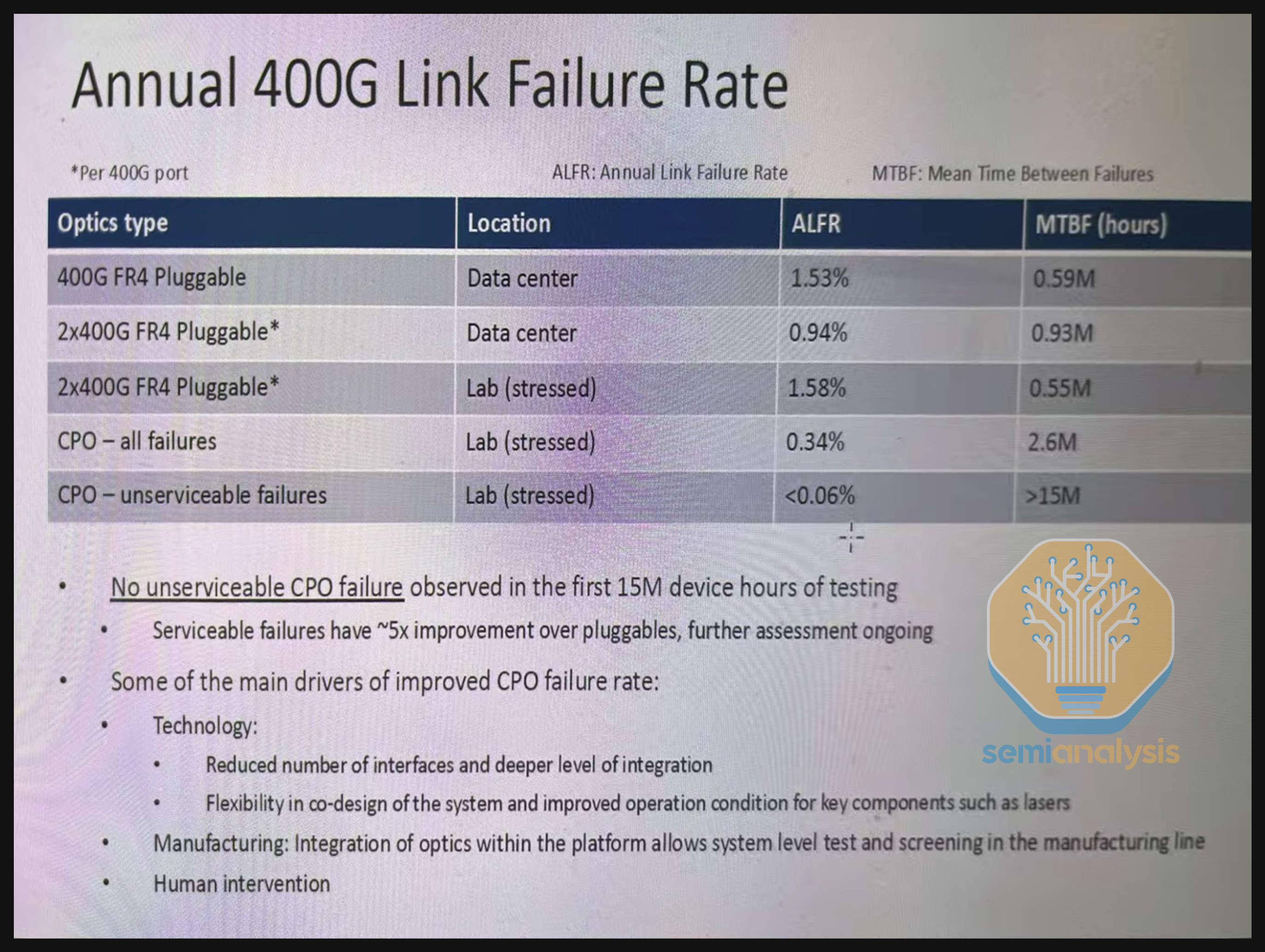
Meta did not stop there, however. In the talk at ECOC presenting the same paper, they presented expanded results for up to 15M 400G port-device hours. These results showed that there were no UCWs for the first 4M 400G port device hours, and they also showed a 0.5-1M device hour mean time before failure (MTBF) for 400G 2xFR4 transceivers (550k for 2xFR4 globally) vs 2.6M device hour MTBF for CPO.
 Source: Meta
While 15M port device hours might sound like a large number, this is in units of 400G port hours. So – one 51.2T switch operated for one hour would mean 128 400G port hours. 15M 400G Port hours across 15 51.2T switches would mean 7,812 wall-clock hours or about 325 days. Indeed, this 15M hour number is often cited as simply “hours” or “device hours” with the “port” part left out. While the zero failure and zero UCW statistic up to 4M port device hours is very helpful – the industry needs far more than just 15 CPO switches tested for 11 months in a lab setting before it pivots towards CPO scale-out switching and commits billions of dollars to this technology.
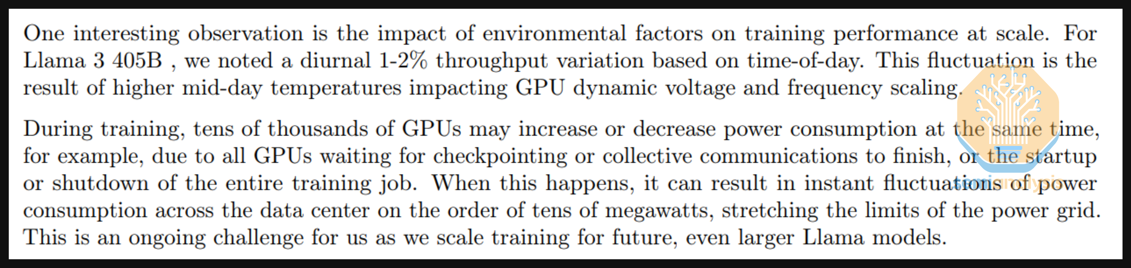
Operating thousands of scale-out switches in a dynamic field environment is entirely different challenge and it remains to be seen how these switches will perform in a production environment. Temperature variation could be higher in a production environment vs a lab, leading to unanticipated variation in component performance or endurance. Meta’s own Llama 3 paper cited 1-2% temperature variations in the datacenter adversely affecting power consumption fluctuations – could such fluctuations affect an entire network fabric in ways that are hard to anticipate?
 Source: Meta
Even mundane sounding problems like dust in a datacenter are the bane of support technicians who can spend considerable time cleaning fiber ends – of course, CPO switches have either an LC or MPO type front pluggable connector, but what about dust inside of the CPO switch chassis? The 0.06% unserviceable failure rate sounds attractive, but such failures have a blast radius of 64 800G ports. This paper is also focused on FR optics based CPO switches, though the next generation of CPO switches will be based on DR optics. These are just a few known unknowns, and there are potentially more unknown unknowns that could come up in field testing.
Indeed, these results have been impactful in terms of convincing those in the industry by delivering tangible reliability data. Our point here is not to create fear, uncertainty or doubt (FUD) but rather to call for even larger scale field testing so that the industry can quickly understand and solve unforeseen problems thereby paving the way for broader CPO adoption, particularly for scale-up networking.
At the end of the day, Nvidia’s scale-out CPO product launch is serving as a practice run and pipe-cleaner for the real high-volume deployment. We think deployment will be far more sizable and impactful for scale up given the much more compelling TCO and Performance/TCO benefit for scale-up vs scale-out.
Moreover - when it comes to scale-out CPO, Rubin Ultra is targeting a launch in 2027 (we think that ends up being late 2027) and the supply chain won’t be ready to ship tens of millions of these CPO endpoints to support GPU demand. Even this timeline is too ambitious for Nvidia. This is why the Feynman generation appears to be the focal point for CPO injection into the Nvidia ecosystem.
Now let’s talk in depth about what CPO is about, the technical considerations, challenges, and state of the ecosystem today.
Part 2: CPO Introduction and Implementation
What is CPO about and why is everyone so excited?
CPO integrates optical engines directly within the same package or module as high-performance computing or networking ASICs. These optical engines convert electrical signals into optical signals, enabling high-speed data transmission over optical links. Optical links must be used for data communication over distances beyond a few meters, as high-speed electrical communication over copper cannot reach beyond a few meters.
Today, most electrical to optical conversion occurs via pluggable optical transceivers. In such cases, an electrical signal will travel tens of centimeters or more from a switch or processing chip through a PCB to a physical transceiver cage at the front plate or back plate of the chassis. The pluggable optical transceiver resides in that cage. The transceiver receives the electrical signal which is reconditioned by an optical Digital Signal Processor (“DSP”) chip and then sent to the optical engine components which convert the electrical signal to an optical signal. The optical signal can then be transmitted through optical fibers to the other side of the link where another transceiver undergoes this process in reverse to turn the optical signal into an electrical signal all the way back to the destination silicon.
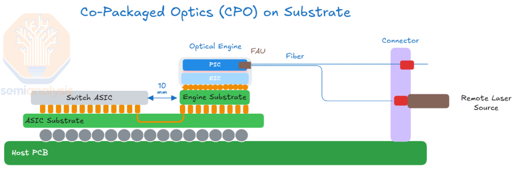
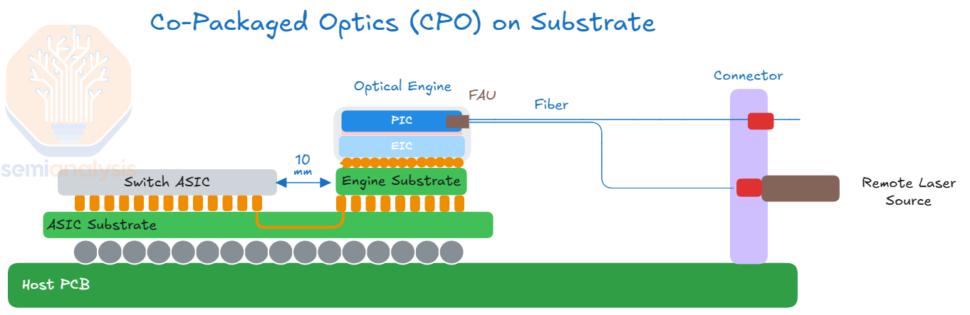
In this process, the electrical signal traverses over a relatively long distances (for copper at least) with multiple transition points before getting to the optical link. This causes the electrical signal to deteriorate and requires a lot of power and complicated circuitry (the SerDes) to drive and recover it. To improve this, we need to shorten the distance the electrical signal needs to travel. This brings us to the idea of “co-packaged optics” where the optical engine that was found in a pluggable transceiver is instead co-packaged with the host chip. This reduces the electrical trace length from tens of centimeters to tens of mm because the optical engine is much closer to the XPU or Switch ASIC. This significantly reduces power consumption, enhances bandwidth density, and lowers latency by minimizing electrical interconnect distances and mitigating signal integrity challenges.
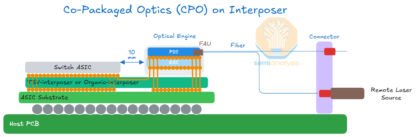
The schematic below illustrates a CPO implementation, where there is an optical engine that resides on the same package as the compute or switch chip. Optical engines will initially be on the substrate, with OEs placed on the interposer in the future.
 Source: SemiAnalysis
 Source: SemiAnalysis
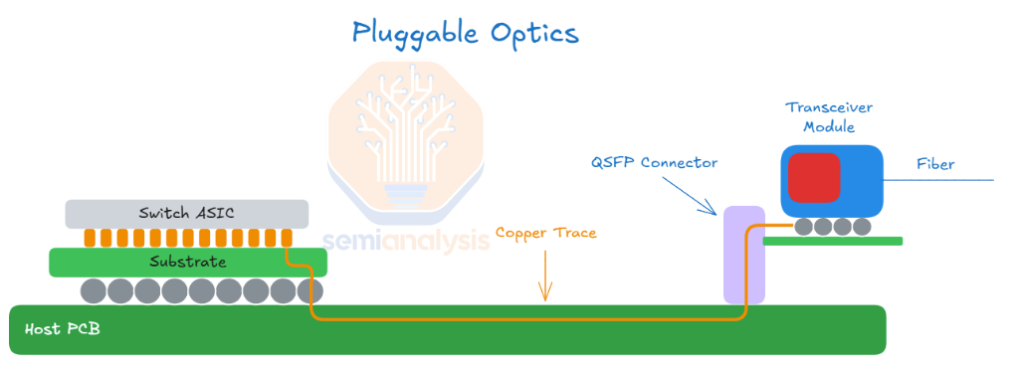
Today, the front pluggable optics solution, as illustrated in the diagram below, is ubiquitous. The main takeaway from this diagram is to illustrate that the electrical signal needs to traverse a long distance (15-30cm) across a copper trace or flyover cable before it gets to the optical engine in the transceiver. As discussed above, this also necessitates the need for long-reach (LR) SerDes to drive to the pluggable module.
 Source: SemiAnalysis
Additionally, there are intermediate implementations that fall between CPO and traditional front-pluggable optics, such as Near-packaged optics (NPO) and On-Board optics (OBO).
In recent years, NPO has emerged as an intermediate step toward CPO. NPO has multiple definitions. NPO is where the OE doesn’t sit directly on the ASIC’s substrate, but is co-packaged onto another substrate. The optical engine remains socketable and it can be detached from the substrate. An electrical signal will still travel from a SerDes on the XPU package through some copper channel to the Optical Engine.
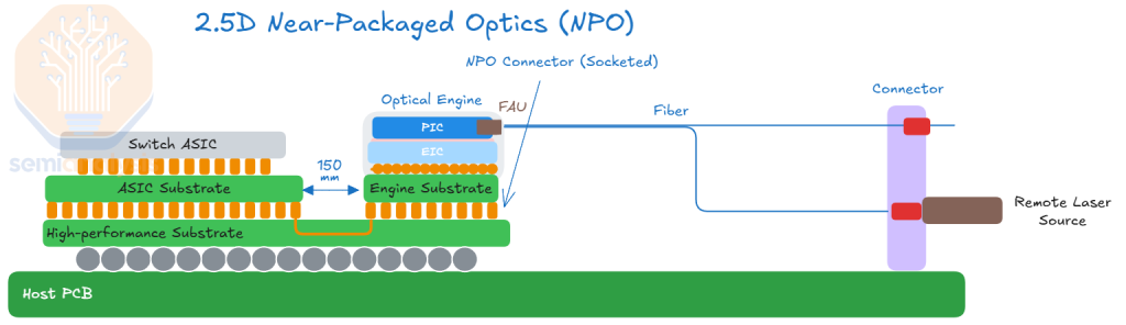 Source: SemiAnalysis
There is also On-Board Optics (OBO), which integrates the optical engine onto the system PCB inside the chassis, positioning it closer to the host ASIC. However, OBO inherits many of the challenges of CPO, while delivering fewer benefits in terms of bandwidth density and power savings. We view OBO as the “worst of both worlds” because it combines the complexity of CPO while inheriting some of the limitations of front-pluggable optics.
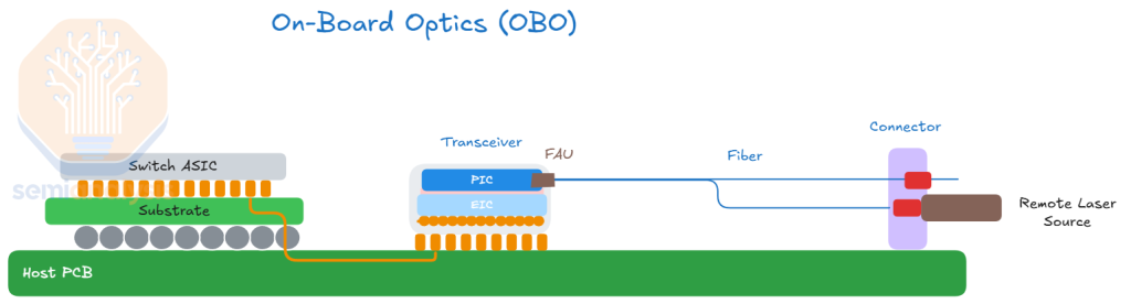 Source: SemiAnalysis
Co-packaged Copper
Another alternative to CPO is “Co-packaged Copper” (CPC). CPC uses copper cabling emerging directly from a connector on substrate. Cables use for CPC are the same cables as flyovers and have the same purpose: to bypass the PCB traces. CPC takes flyover cables further with the socket starting on the package substrate itself. The cables used are twin-axial cables (Twinax cables) that are well insulated to reduce cross-talk, resulting in significantly lower insertion loss compared to conventional electrical traces. Though this solution still uses copper, it offers a key advantage in signal integrity. CPC could provide a practical path to deploying 448G SerDes so as to allow another scaling of off-package interconnect.
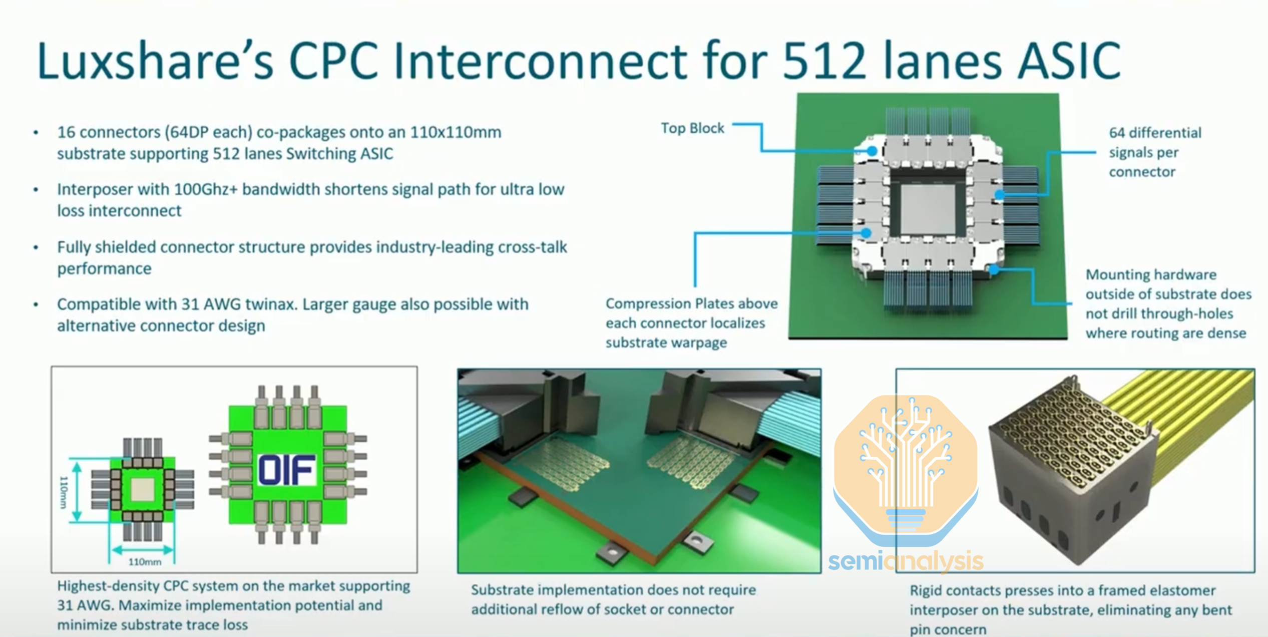 Source: LuxShare
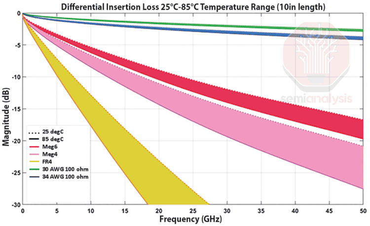 Source: Luxshare
The challenge with CPC lies in the added complexity of the package substrate. The substrate must route power and signals to thousands of these cables. Despite this challenge, CPC remains significantly simpler than CPO, which still has to overcome a number of manufacturing hurdles across multiple parts of the supply chain. We see CPC as particularly attractive for some short-reach applications such as in-rack scale up connectivity, which we will explore below. By bypassing lossy CCL traces, CPC could be the technology that enables 448G line speeds. CPC is also being looked at very broadly for enabling 448G as signals of this bandwidth experience unacceptable attenuation when running through PCBs.
Past obstacles to CPO market readiness: Why only now?
Despite its technical superiority, CPO has seen very limited real-world adoption due to several challenges that drive up cost. These include: the complexity of packaging (which costs more than the OEs themselves) and manufacturing, reliability and yield concerns, as well as thermal management issues arising from tightly integrated optical and electrical components. Another hang-up is the lack of industry-wide standardization. Additionally, customers are concerned about serviceability which hinders the transition from traditional pluggable optics to CPO solutions.
Another key customer anxiety is that by adopting CPO, they potentially surrender their ability to control costs. It is much easier to squeeze a larger number of transceiver companies on costs than a smaller set of switch vendors.
Meanwhile, pluggable optics—the incumbent technology that CPO would replace—continue to improve and still offers good enough performance for nearly all applications with far less end user anxiety.
In the remainder of Part 2, we will dive further into the impetus for adopting CPO. We will start with explaining how SerDes scaling is reaching a plateau, making other interface types such as Wide I/O coupled with CPO necessary, and then step into manufacturing considerations and go to market. We will discuss key individual CPO component such as Optical Engines, Fiber Coupling, External Laser Sources and Modulators. Lastly, we will cover the roadmap for scaling bandwidth from CPO.
Evolving beyond DSP-based Transceivers: From LPO to CPO
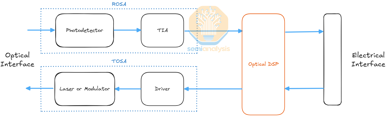
DSP Transceivers handle both the transmission and reception of optical signals and contain an “optical engine” (OE) which is responsible for electro-optical conversion. The OE consists of a driver (DRV) and modulator (MOD) to transmit optical signals, and a transimpedance amplifier (TIA) and photodetector (PD) to receive optical signals.
Another important component is the optical DSP chip, which sometimes integrates the Driver and/or TIA into one package. The high frequency electrical signal that is transmitted from the host switching or processing chip needs to travel a relatively long distance over lossy copper traces to reach the transceiver at the front of the server chassis. The DSP is responsible for retiming and reconditioning this signal. It carries out error correction and clock/data recovery to compensate for electrical signal degradation and attenuation as the signal passes from the switch or ASIC silicon through the substrate or other transmission medium. For modulation, in the case of PAM4 Modulation (Pulse Amplitude Modulation with 4 Levels), the DSP maps a binary signal into four distinct amplitude levels in order to increase the number of bits per signal, allowing higher bitrates and more bandwidth.
 Source: SemiAnalysis
The DSP chip is one of if not the most power-hungry and expensive components within the transceiver. For an 800G SR8 Transceiver – the DSP accounts for nearly ~50% of the module’s total power consumption, which is why there has been so much focus on getting rid of the DSP.
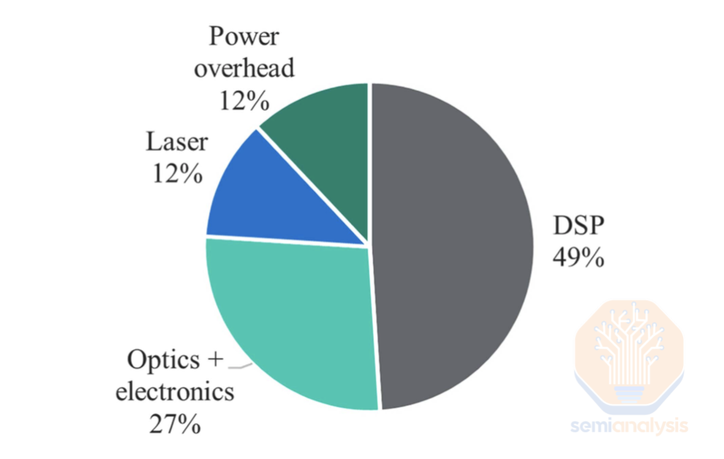
An 18k GB300 Cluster build with a two-layer InfiniBand network will require 18,432 800G DR4 transceivers and 27,648 1.6T DR8 transceivers. The extra cost and power requirements stemming from the use of DSPs can add considerably to the total cost of ownership. Budgeting 6-7W for the 800G DSP and 12-14W for the 1.6T DSP, this would add up to 480kW of DSP power for just the back-end network alone for this entire cluster, or about 1.8kW per server rack. When sourced from premium brand-name suppliers, transceivers can account for nearly 10% of the cluster’s total cost of ownership. So – accounting for 50% of the power draw and 20-30% of the BoM of a typical transceiver – some regard DSPs as public enemy number one of cost and power efficiency.
 Source: SemiAnalysis AI Networking Model
The Crusade Against DSPs
The high cost and power proportion taken up by DSPs has motivated the industry to find technologies that can disintermediate the DSP. The first wave of attack on the DSP was linear pluggable optics (LPO) – which attempt to remove the DSPs altogether and have the SerDes from the switches directly drive the TX and RX optical elements in the transceiver. However, LPO has not yet taken off as DSP Diviner Loi Nguyen correctly predicted in our interview with him back in 2023.
CPO takes the LPO concept to the next step by placing the optical engine on the same package as the compute or switch chip. A key benefit of CPO is that the DSP that was found in the transceiver is no longer required because the distance between the host and the optical engine is so short. CPO also goes further than LPO because it unlocks much greater chip shoreline density by eliminating the need for power and area-hungry LR SerDes in favor of shorter reach SerDes or even clock forwarded wide D2D SerDes in the case of wide I/O interface.
The oft-cited expression is that CPO has been just around the corner for the last two decades – but why has it failed to take off for so long. Why has the industry preferred to stick with pluggable DSP transceivers?
One key advantage of pluggable transceivers is their high interoperability. With standard form factors such as OSFP and QSFP-DD and adherence to OIF standards, customers can generally select transceiver vendors independent of switch and server vendors, enjoying procurement flexibility and stronger bargaining power.
Another huge advantage is field serviceability. Installing and replacing transceivers is simple as they can be unplugged from a switch or server chassis by a pair of remote hands. In contrast, with CPO any failures in the optical engine could render the entire switch unusable. Even serviceable failures could be complicated to troubleshoot and fix. Often, the laser is the most common point of failure, and most CPO implementations now use pluggable external laser source for better serviceability and replaceability, but anxiety remains regarding the failure of other non-pluggable CPO components.
Why CPO? The I/O challenge, BW density, and bottlenecks
Other than getting rid of power hungry and costly DSPs and minimizing or eliminating the use of LR SerDes, the other huge benefit of adopting CPO is greater interconnect bandwidth density relative to energy consumption.
Bandwidth density measures the amount of data transferred per unit area or channel, reflecting how effectively limited space can be utilized for high-speed data transmission. Energy efficiency quantifies the energy required to transmit a unit of data.
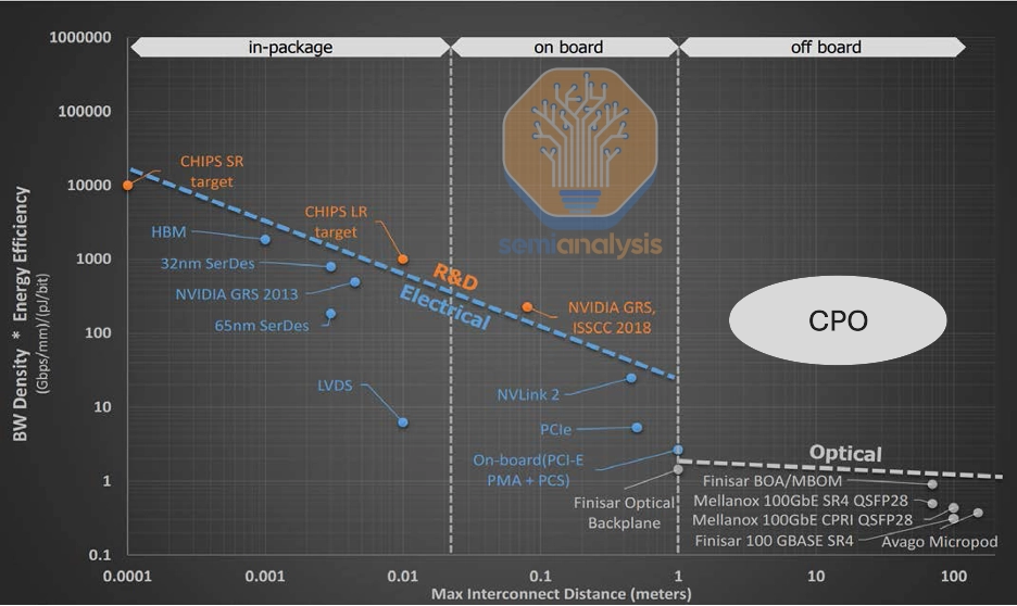
Thus, interconnect bandwidth density relative to energy consumption is a very important figure of merit (FoM) when determining the objective quality of a given interconnect. Of course, the optimal interconnect is the one that also fits within distance and cost parameters.
When examining the chart below, a clear trend emerges: this figure of merit degrades exponentially for electrical links as distance increases. Also, moving from purely electrical interfaces to those requiring optical–electrical conversion introduces a substantial drop in efficiency—potentially by an order of magnitude. This drop is caused because it requires energy to drive signals some distance from the chip to the front-panel where the transceiver is. It requires even more energy to power optical DSPs. The figure of merit curve for CPO-based communication lies squarely above pluggables. As indicated in the chart below, CPO offers more bandwidth density per area per energy consumed over the same ranges of distance making it an objectively better interconnect.
 Source: G Keeler, DARPA 2019, SemiAnalysis
This chart also illustrates the adage “use copper where you can and optical when you must.” Shorter reach communication over copper is superior when available. Nvidia embraces this mantra with their rack-scale GPU architectures architected solely for the purpose of pushing the limits of intra-rack density to maximize the number of GPUs that can be networked together over copper. This is the rationale behind the scale-up network architecture used for the GB200 NVL72, and Nvidia is taking this idea even further in their Kyber rack. However – it is only a matter of time until CPO’s maturity makes accessing its part of the FoM curve viable for scale-up and worth it from a performance per TCO perspective.
Input/Output (I/O) Speedbumps and Roadblocks
While transistor densities and compute (as represented by FLOPs) have scaled well, I/O has scaled much more slowly, creating bottlenecks in overall system performance: there is only so much usable shoreline available for off-chip I/O as the data that goes off-chip needs to escape over a limited number of I/Os on the organic package substrate.
Additionally, increasing the signaling speed of each individual I/O is becoming increasingly challenging and power-intensive, further constraining data movement. This is a key reason why interconnect bandwidth has scaled so poorly over the past many decades relative to other computing trends.
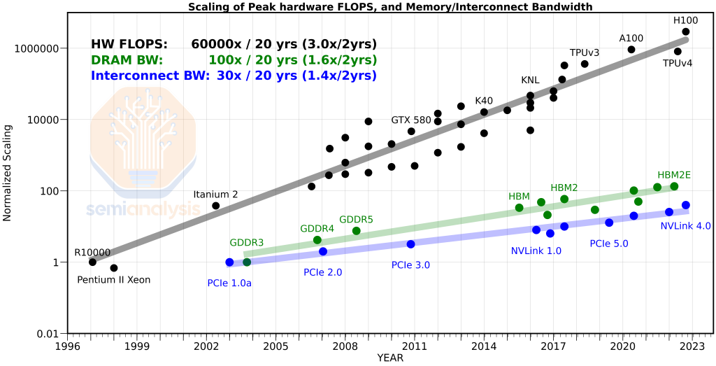 Source: Amir Gholami
Off-package I/O density for HPC applications has plateaued due to limitations on the number of bumps in a single flip-chip BGA package. This is a constraint on scaling escape bandwidth.
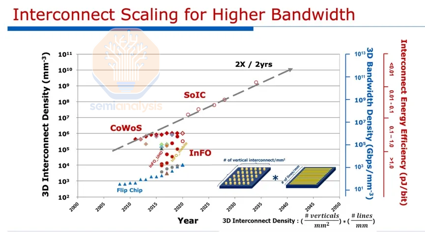 Source: TSMC
Electrical SerDes Scaling Bottlenecks
With limited number of I/Os, the way to realize more escape bandwidth is to push the frequency that each I/O signals at. Today, Nvidia and Broadcom are at the leading edge of SerDes IP. Nvidia shipping 224G SerDes in Blackwell which is what enables their blazing fast NVLink. Similarly, Broadcom has been sampling 224G SerDes since late 2024 in their optical DSPs. It’s no coincidence that the two companies that ship the most AI FLOPs in the industry also lead in high-speed SerDes IP. This reinforces the fundamental connection between AI performance and throughput, where maximizing data movement efficiency is just as critical as delivering raw compute power.
However, it is becoming increasingly challenging to provide higher line speeds at a desirable reach. As frequencies increase, insertion losses rise, as shown in the chart below. We see that losses increase at higher SerDes signaling speeds especially as the signal path lengthens.
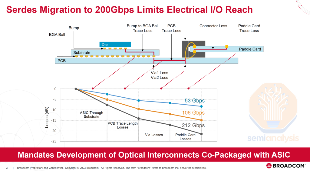 Source: Broadcom
SerDes scaling is approaching a plateau. Higher speeds can only be sustained over very short distances without additional signal recovery components—which in turn increase complexity, cost, latency, and power consumption. It has been difficult to get to 224G SerDes.
Looking ahead to 448G SerDes, the feasibility to drive beyond just a few centimeters remains more uncertain. Nvidia is delivering 448G per electrical channel connectivity in Rubin by using a bi-directional SerDes technique. Achieving true 448G uni-directional SerDes will require further development. We may need to move to higher orders of modulation such as PAM6 or PAM8 instead of the PAM4 modulation which has been prevalent since the 56G SerDes era. Using PAM4, which encodes 2 bits per signal, to get to 448G will require a baud rate of 244Gbaud that is likely untenable due to excessive power consumption and insertion loss.
SerDes Scaling Plateau as a Roadblock for Scaling NVLink
In the NVLink protocol, bandwidth in NVLink 5.0 has increased more than 11x compared to NVLink 1.0. However, this growth has not come from a significant increase in lane count, which has only risen slightly from 32 lanes in NVLink 1.0 to 36 lanes in NVLink 5.0. The key driver of scaling has been a 10x increase in SerDes lane speed, from 20G to 200G. In NVLink 6.0, however, Nvidia is expected to stay on 200G SerDes, meaning it will have to deliver a doubling in lane count - it delivers on this cleverly by using bi-directional SerDes to effectively double the number of lanes while using the same number of physical copper wires. Beyond this, scaling either SerDes speed and overcoming limited shoreline availability to fit more lanes lane count will become increasingly difficult and total escape bandwidth will be stuck.
Scaling escape bandwidth is critical for companies at the leading edge where throughput is a differentiator. For Nvidia, whose NVLink scale up fabric is an important moat, this roadblock could make it easier for competitors such as AMD, and the hyperscalers to catch up.
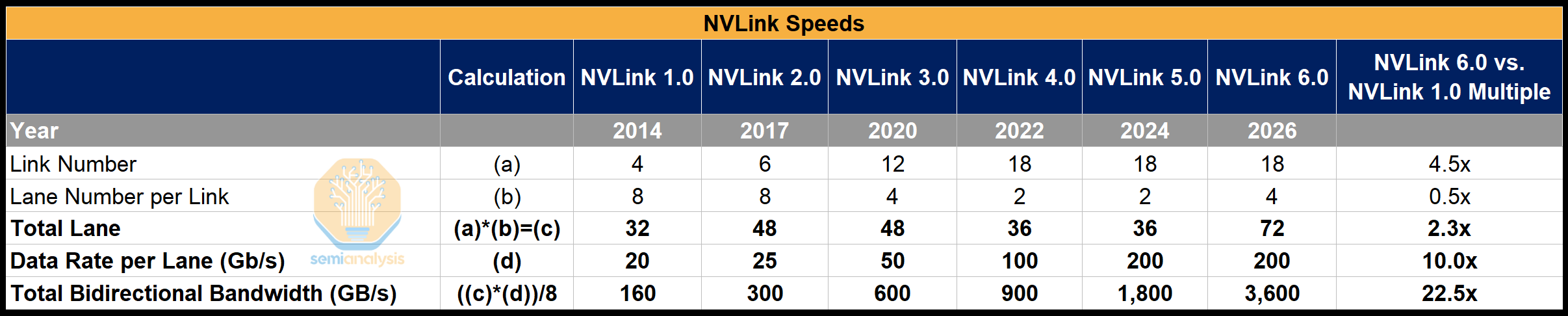 Source: Nvidia, SemiAnalysis
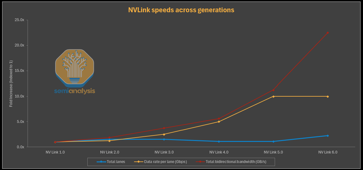 Source: Nvidia, SemiAnalysis
The solution to this dilemma – or put another way the necessary compromise – is to shorten the electrical I/O as much as possible and offload data transfer to optical links as close to the host ASIC as possible to achieve higher bandwidths. This is why CPO is considered the “holy grail” of interconnect. CPO allows optical communication to happen on the ASIC package, whether via the substrate or the interposer. Electrical signals only need to travel over a few millimeters through the package substrate, or ideally an even shorter distance through a higher quality interposer, rather than tens of centimeters through lossy copper-clad laminate (CCL).
The SerDes can instead be optimized for shorter reach which needs much less circuitry than equivalent long reach SerDes. This makes it easier to design while consuming less power and silicon area. This simplification makes higher-speed SerDes easier to implement and extends the SerDes scaling roadmap. Nonetheless, we remain constrained by the traditional bandwidth model, where bandwidth density continues to scale in proportion to SerDes speed.
To achieve much higher B/W density, wide I/O PHYs are a better option over extremely short distances, offering better bandwidth density per power consumed than SerDes interfaces. Wide I/Os also come at the cost of a much more advanced package. However, in the case of CPO, this is a moot point: the packaging is already highly advanced, so integrating wide I/O PHYs adds little to no additional packaging complexity.
Wide I/O vs SerDes
Once there is no longer a requirement to drive electrical signals to relatively long distances, we can escape serialized interfaces altogether by using wide interfaces that offer much better shoreline density over short distances.
One such example is with UCIe interface. UCIe-A can offer up to ~10 Tbit/s/mm of shoreline density, which is designed for advanced packages (ie. chiplets interfacing via an interposer with sub-2mm reach). On a long edge of a reticle sized chip this is up to 330 Tbit/s (41TByte/s) of off-package bandwidth. This is 660 Tbit/s of bi-directional bandwidth off of both edges. This compares to Blackwell which only has 23.6 Tbit/s of off-package BW, equivalent to around 0.4 Tbit/s/mm of shoreline density, which is a big difference.
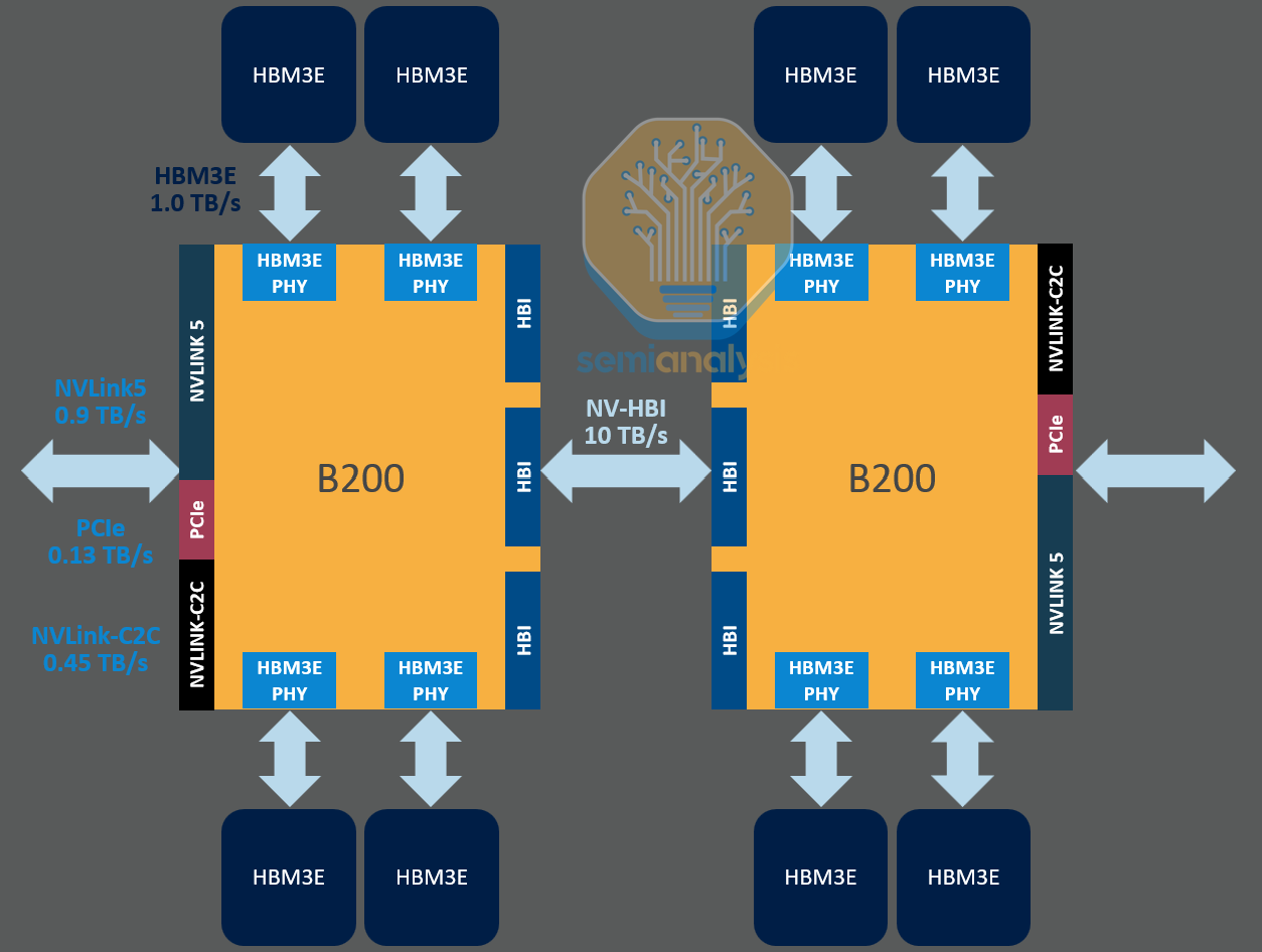 Source: SemiAnalysis
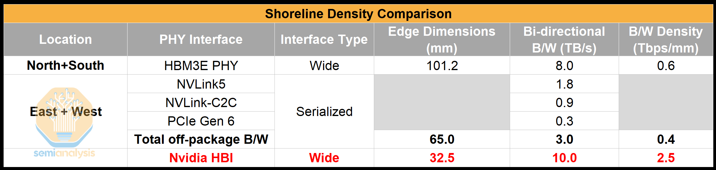 Source: SemiAnalysis
Of course – this is not a like-for-like comparison as these off-package PHYs are needed to drive a long distance. If anything, this is the very point that is being illustrated: with CPO, reach is no longer a consideration as signals are not being driven long distances electrically. At bandwidth densities of 10 Tbit/s/mm, the bottleneck is no longer on the electrical interface but at other parts of the link, namely how much bandwidth can escape on the fibers on the other side.
Getting to this constraint is an end state very far away from today’s reality and the OE will have to share an interposer with the host. Integrating CPO on the interposer itself is even farther off on the roadmap than reliably integrating OEs on the substrate. PHY performance on the substrate is of course inferior with UCIe-S offering about 1.8Tbit/s/mm of shoreline density. This is still a significant uplift over what we believe 224G SerDes offers at ~0.4 Tbit/s/mm.
However, Broadcom and Nvidia are persisting with electrical SerDes on their roadmap despite the advantages a wide interface offers. The primary reason is they believe they can still scale SerDes and that they need to design for copper especially as adoption for optics is slow. It also appears more likely that hybrid co-packaged copper and co-packaged optics solutions will be here to stay, requiring them to optimize for both. This approach is taken so as to eliminate the need for multiple tape-outs for different solutions.
Link Resiliency
Link resiliency and reliability are other very important driving factors of CPO technology. In large AI clusters, link downtime is a significant contributor to overall cluster availability, and even small improvements in link availability and stability provides large return on infrastructure investment.
Today, in a large-scale AI cluster approaching 1M links with pluggable modules, there can be dozens of link interruptions per day. Some of these are ‘hard’ failures as a result of component failures or hardware quality, while many of these are ‘soft’ failures resulting from a diversity of root causes that results from the inherent complexity and variability of pluggable-based solutions. There is a long tail of failure modes, including but not limited to signal integrity issues and variation, connector and wirebond quality, contamination on components and pins, noise injection, and other transient effects. There is little correlation with component failures. 80% of optical modules that are returned due to some link failure are ‘no trouble found’.
CPO significantly reduces the inherent complexity and variability of the high-speed signal paths in large-scale AI networks by:
- Significantly reducing the number of components in the optical interface. High levels of integration at both the photonic level and chip/package level reduce the complexity for critical high-speed assemblies and improve the reliability and yield at the system level. The number of E/O interfaces is also reduced, thereby minimizing the power loss that occurs at each interface
- Significantly improving the signal integrity of the host electrical interface between the host ASIC (e.g. switch) and the optical engine. Insertion losses, reflections and other non-linear impairments are significantly reduced by packaging the optical engine on the first level package with very well defined and deterministic design rules and manufacturing tolerances
- Reducing the port-to-port variation in high-speed signal path across the switch, which adds overhead and complexity to DSP signal processing, host and module equalization, host and module firmware and link optimization algorithms. All pluggable module solutions, and the host SerDes, must be designed to accommodate this variation in per-port performance which leads to complexity and points of failure
Removing the ‘human’ element of optical link provisioning. A CPO switch or optical engine is fully assembled and tested ‘known-good’ out of the factory and does not require significant on-site operations to provision the optics in the switch, which can lead to installation variation, damage, contamination, and compatibility issues between systems and optical modules.
Part 3: Bringing CPO to Market and deployment challenges
CPO optical engine manufacturing considerations and go to market
CPO has not yet been manufactured at quantities commensurate with wide-scale adoption. Broadcom was the only vendor to have shipped production systems featuring CPO, with its Bailly and Humboldt switches, but now Nvidia is joining the fray. These have been shipped at very low volumes. CPO introduces many new manufacturing processes and significant manufacturability challenges. Understandably, given the immaturity of the supply chain and lack of data on reliability, customers are also reluctant to take the plunge in adopting the technology.
For CPO to gain traction, an industry leader must invest in shipping these products, driving the supply chain to develop scalable manufacturing and testing processes. Nvidia is the one taking the plunge and their intention is to get the supply chain ready, identify and work out the issues, and prepare datacenter operators for what we think will be the ‘killer’ application: Scale-up networking. There are a few key components and considerations to focus on regarding CPO, all of which have implications on performance and manufacturability. These are:
- Host and Optical Engine packaging
- Fibers and Fiber coupling
- Laser Sources and Wavelength Multiplexing
- Modulator Type
Host and Optical Engine Packaging
As the name suggests, “Co-packaged optics”, is fundamentally a packaging and assembly challenge.
An optical engine has both optical and electrical components. The photodetector and modulators are optical components contained in the contained in the “PIC” (photonic integrated circuit). The Driver and Transimpedance Amplifier are electrical circuitry contained in the “EIC” (electric integrated circuit). The PIC and EIC need to be integrated for the OE to function. Multiple packaging methods exist to accomplish this PIC–EIC integration.
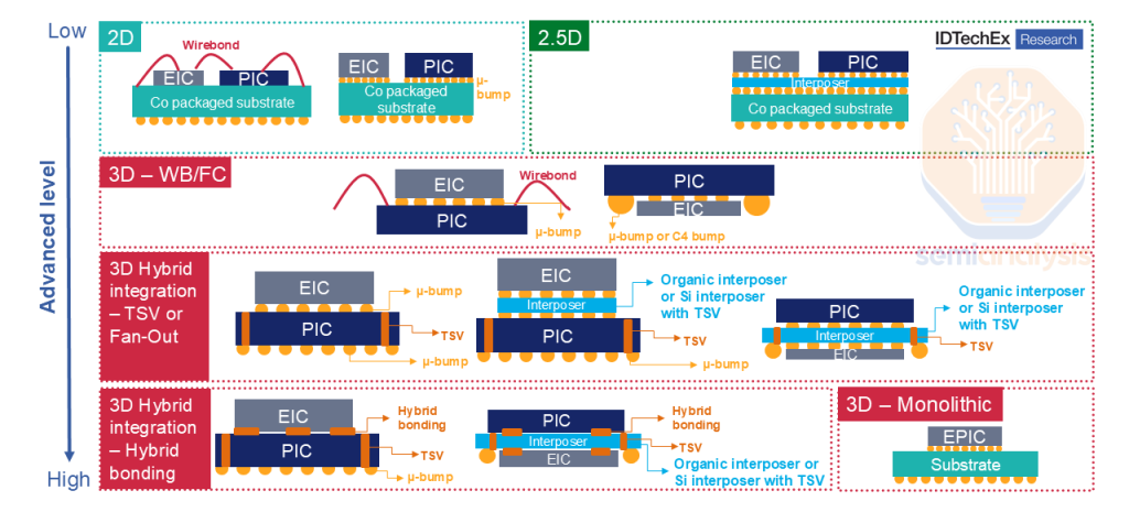 Source: ID TechEx
Optical engines can be monolithic by having both the PIC and EIC manufactured on the same silicon wafer. Monolithic integration is the most elegant approach in terms of parasitics, latency, and power. This is the approach taken by Ayar Labs for their second-gen TeraPHY chiplet (though their next-gen chiplet does pivot to TSMC COUPE). GlobalFoundries, Tower and Advanced Micro Foundry are foundries that can offer a monolithic CMOS and SiPho process. However, monolithic processes stop at geometries below around 35nm as photonics processes cannot scale like traditional CMOS. This limits the EIC’s capabilities, especially with the higher lane speeds expected in CPO systems. Despite the inherent simplicity and elegance, this makes monolithic integration a dealbreaker for scaling. This is why Ayar Labs is also moving their roadmap to heterogeneously integrated OEs to allow for further scaling.
Heterogenous integration is becoming the mainstream approach which involves fabricating the PIC using a SiPho process and integrating that with an EIC from a CMOS wafer through advanced packaging. Various packaging solutions exist, with more advanced packaging solutions delivering higher performance. Among them, 3D integration offers the best bandwidth and energy efficiency. A big issue when it comes to EIC to PIC communication is parasitics which erodes performance. Reducing trace length drastically reduces parasitics and therefore coupling efficiency: 3D integration is the only way to reach the performance goals of CPO from a bandwidth and power perspective.
TSMC COUPE is emerging as the integration option of choice
TSMC is racing ahead as the foundry partner of choice for the next generation of OEs for both the fabless giants and startups. The first high-volume products featuring CPO endpoints are being introduced under the name “COUPE” - short for “Compact Universal Photonic Engine”. This includes the fabrication of EICs and PICs, as well as heterogeneous integration under TSMC’s COUPE solution. Nvidia proudly displayed their COUPE optical engines at GTC 2025, and these will be the first COUPE products to ship. Broadcom is also adopting COUPE for their future roadmap, despite having existing generations of their OEs with other supply chain partners. As mentioned earlier, Ayar Labs, who has previously relied on Global Foundries’ Fotonix platform for monolithic optical engines, now also has COUPE on their roadmap.
Unlike its dominance in traditional CMOS logic, TSMC previously had a limited presence in silicon photonics, where Global Foundries and Tower Semi were the preferred foundry partners. However, in recent years, TSMC has been quickly catching up when it comes to their photonic capabilities. TSMC also brings its unquestionable strength in leading edge CMOS logic for the EIC component, as well as its leading packaging capabilities – TSMC is the only foundry that has successfully demonstrated die-to-wafer hybrid bonding capabilities at reasonable scale, having shipped various AMD hybrid bonded chips in volume. Hybrid bonding is a more performant approach to bond the PIC and EIC, though it does comes with a significantly higher cost. Intel is working to develop a similar capability but has faced significant challenges in pioneering this technology.
Overall, TSMC has now become a very key player in CPO despite its previously weaker standalone SiPho capabilities. Like other major players, TSMC aims to capture as much of the value chain as possible. By adopting TSMC’s COUPE solution, customers effectively commit to using TSMC-manufactured PICs, as TSMC does not package SiPho wafers from other foundries. Many CPO focused companies have indeed pivoted decisively towards making TSMC’s COUPE as part of their go to market solution for the next few years.
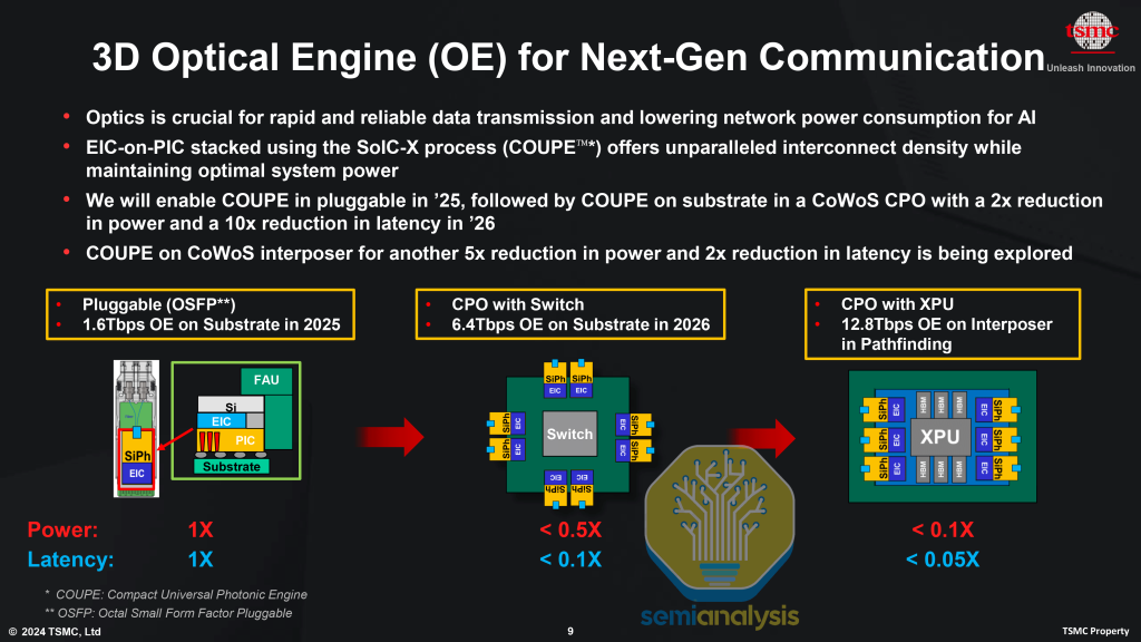 Source: TSMC
Die fabrication: TSMC offers a comprehensive suite of solutions for die fabrication. The EIC is manufactured on the N7 node, integrating high-speed optical modulator drivers and TIAs. It also incorporates heater controllers to enable functions such as wavelength stabilization. The PIC, on the other hand, is fabricated on the SOI N65 node, and TSMC provides extensive support for photonic circuit design, photonic layout design and verification, as well as simulation and modeling of photonic circuits (which covers aspects such as RF, noise, and multi-wavelength).
EICs and PICs are bonded using the TSMC-SoIC-bond process. As we mentioned previously, longer trace lengths mean more parasitics, which degrades performance. TSMC’s SoIC is a bumpless interface offering the shortest trace length possible without being monolithic and is therefore the most performant possible way to heterogeneously integrate the EIC and PIC. As shown below, at iso-power, SoIC based OEs offer more than 23x the bandwidth density of an OE integrated with bumps.
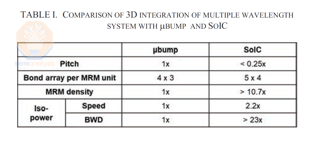 Source: TSMC
COUPE supports the whole optical engine design and integration process. For optical I/O, it supports µLens design, enabling the integration of micro-lenses at the wafer or chip level, as well as optical I/O path simulations covering mirrors, µLenses, grating couplers (GC), and reflectors. For 3D stacking, it supports 3D floorplanning, SoIC-X/TDV/C4 bump layout implementation, interface physical checking, and high-frequency channel model extraction and simulation. To ensure seamless development, the company provides a complete PDK and EDA workflow for COUPE design and verification, enabling designers to implement their technologies efficiently.
Coupling: As we will detail more later, there are two main coupling methods – grating coupling (GC) and edge coupling (EC). COUPE uses one common EIC on PIC bumpless stacking structure for both GC and EC. However, the COUPE-GC structure will distinctively use Silicon lens (Si lens) and MR (metal reflector), while COUPE-EC will uniquely have EC facet (for terminating EC to fiber). In the case of GC, the Si lens is designed on a 770µm silicon carrier (Si-carrier) and the MR is positioned directly underneath the GC, along with the optimization dielectric layers required for optical performance. The Si-carrier is then WoW (wafer-on-wafer) bonded to a CoW (chip-on-wafer) wafer.
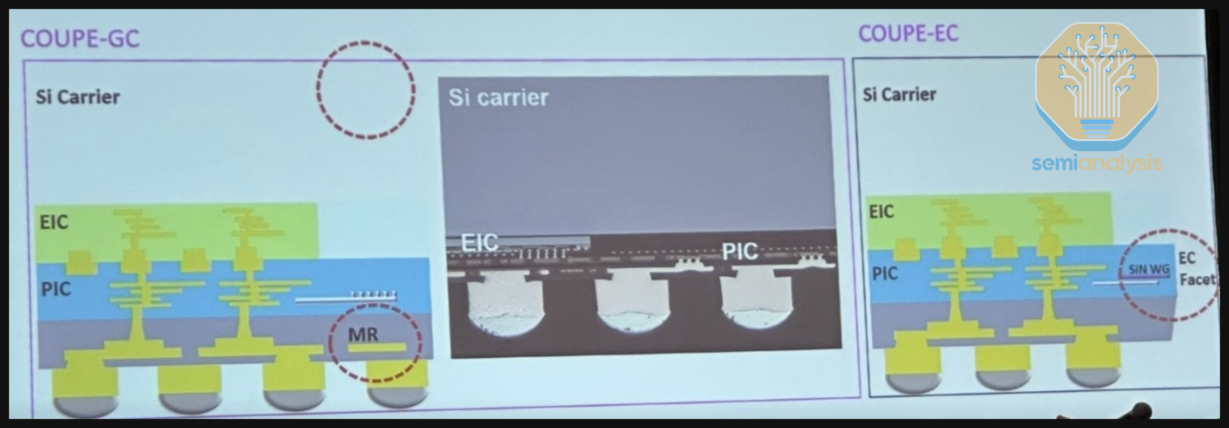 Source: TSMC
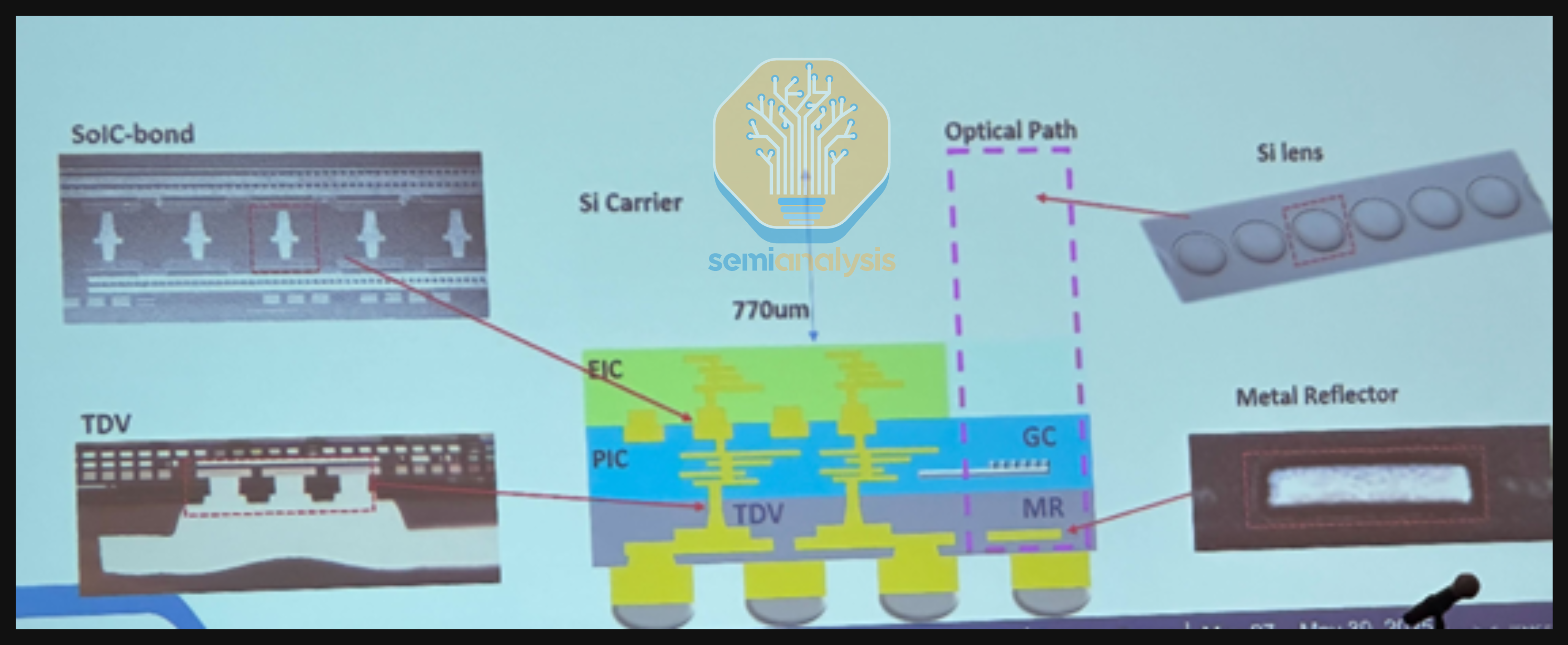 Source: TSMC
Fiber Attach Unit (FAU): The FAU needs to be co-designed according to the optical path of COUPE. The purpose of the FAU is to couple the light from Si lens into the optical fiber at low insertion loss. The manufacturing difficulty increases as number of I/O increases, but development time and costs are reduced if industry can adhere to specific standards. Overall, each component requires an optimized design to achieve the best optical performance.
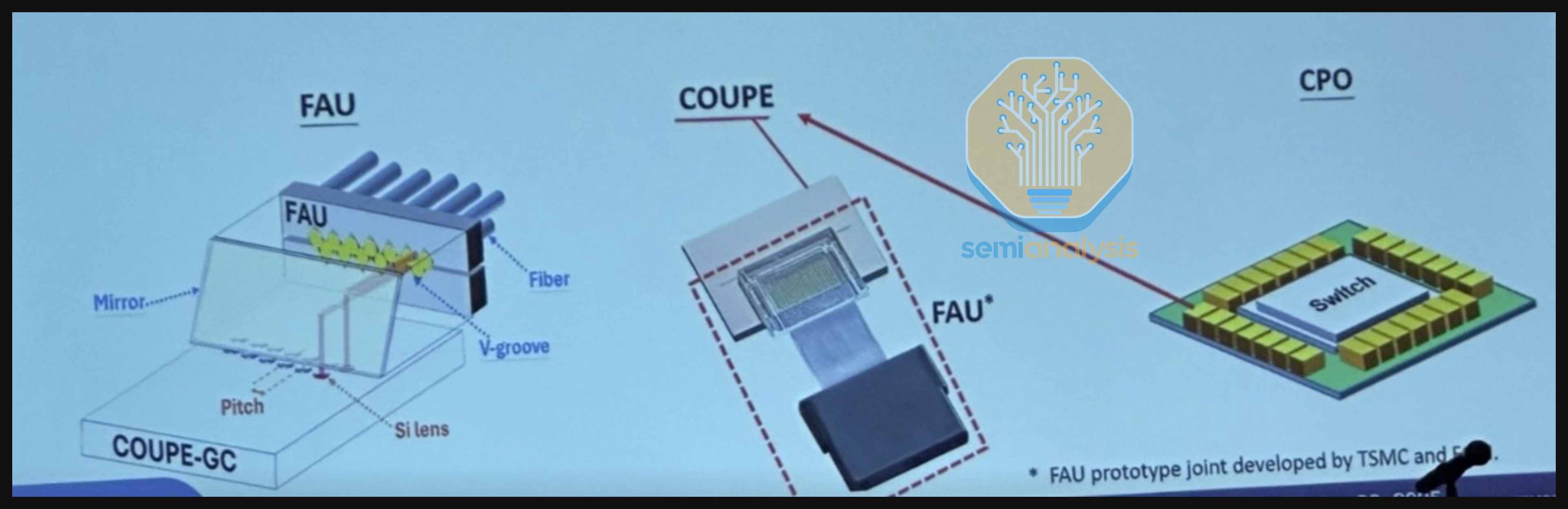 Source: TSMC
Product roadmap: The first iterations of COUPE will be optical engines on the substrate with the ultimate goal being able to put the OEs on the interposer. The interposer offers far more I/O density, therefore enabling greater bandwidth between the OEs and the ASIC PHYs, with the possibility of individual OEs having up to 12.8Tbit/s of bandwidth each, translating to approximately 4 Tbit/s/mm. The challenge for integrating the interposer is scaling the interposer size (which is more expensive than the package substrate) to accommodate the OE.
This is why Broadcom is transitioning to TSMC COUPE for its CPO solutions, despite having iterated multiple generations of CPO using a Fan-Out Wafer-Level Packaging (FOWLP) approach developed by SPIL. Notably, Broadcom has committed to COUPE for its future switch and customer accelerator roadmaps. We understand that the FOWLP approach doesn’t allow scaling beyond 100G per lane due to excessive parasitic capacitance, as electrical signals must pass through the Through-Mold Vias (TMV) to get to the EIC. To maintain a competitive roadmap, Broadcom must transition to COUPE, which offers superior performance and scalability. This highlights TSMC’s technological edge, enabling them to secure wins even in optics, a domain where they have historically been considered weaker.
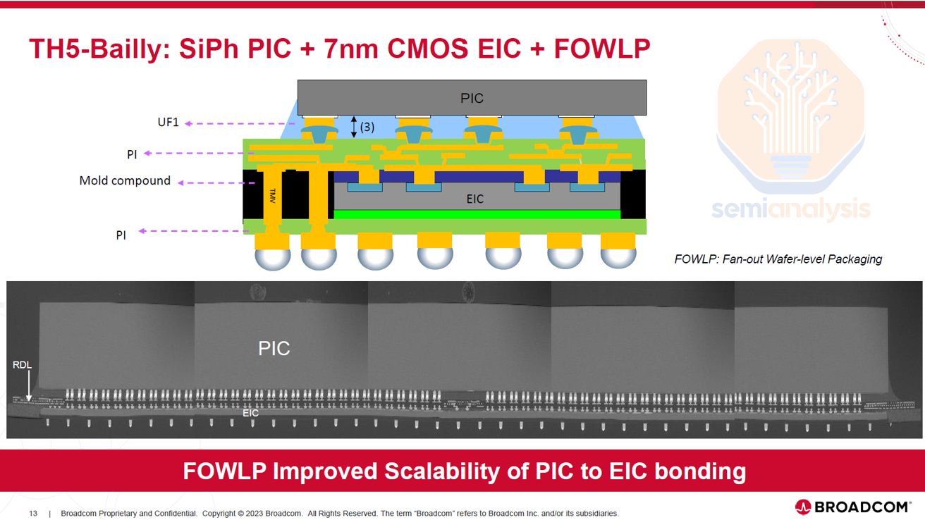 Source: Broadcom
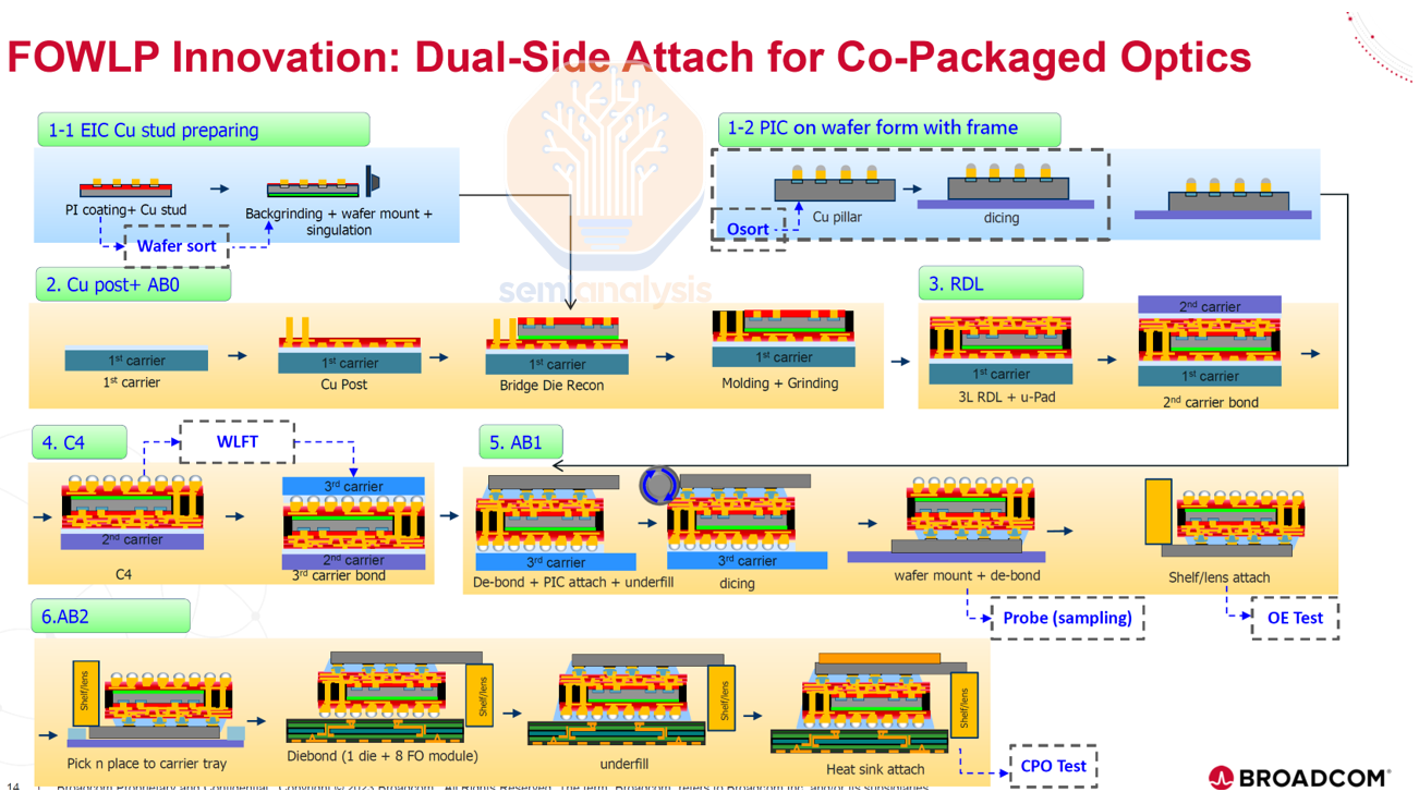 Source: Broadcom
Packaging the OEs with the host
The OEs themselves are placed on a substrate, after which the substrate is flip-chip bonded to the host package. For co-packaging the OEs a lot of package area is required. This necessitates significantly enlarging either the package substrate or interposer, depending on where it is placed. For Nvidia’s Spectrum-X Photonics switch ASIC package, the substrate will measure 110mm by 110mm. For context, this compares to the Blackwell package at 70mm by 76mm which is a very big chip in its own right.
Additionally, attaching more elements to the substrate presents yield challenges. Again, for Spectrum-X, 36 known good OEs need to be flip-chip bonded onto the substrate first – before bonding the interposer module for the ‘on Substrate’ step to complete the CoWoS assembly.
Similarly, for the interposer, the need to manufacture a much larger interposer is costly and it requires bonding many more elements, presents yield challenges. Additionally, these challenges are exacerbated by warpage issues, which become more pronounced as interposer/substrate size scales.
FAUs and Fiber Coupling
Fibers come out of the OE for the data to transmit. One optical lane is comprised of two fibers or one fiber pair (transmit plus receive). Fiber coupling – aligning the fibers precisely with on-chip waveguides for smooth and efficient light transmission – is a crucial and challenging step in CPO, and Fiber Array Units (“FAUs”) are widely used in CPO to assist in that process. There are two main ways to do this, namely edge coupling (EC) and grating coupling (GC).
Edge Coupling
Edge coupling aligns the fiber along the chip’s edge. From the image below, we can see that the fiber end must be precisely aligned with the polished edge of the chip to ensure that the light beam enters the edge coupler accurately. A microlens at the fiber tip focuses and directs the light toward the chip, leading its entry into the waveguide. The waveguide taper gradually widens, allowing for a smooth mode transition that reduces reflections and scattering to ensure coupling efficiency. Without such a lens and taper, there will be significant optical loss at the interface between fiber facet and waveguide facet.
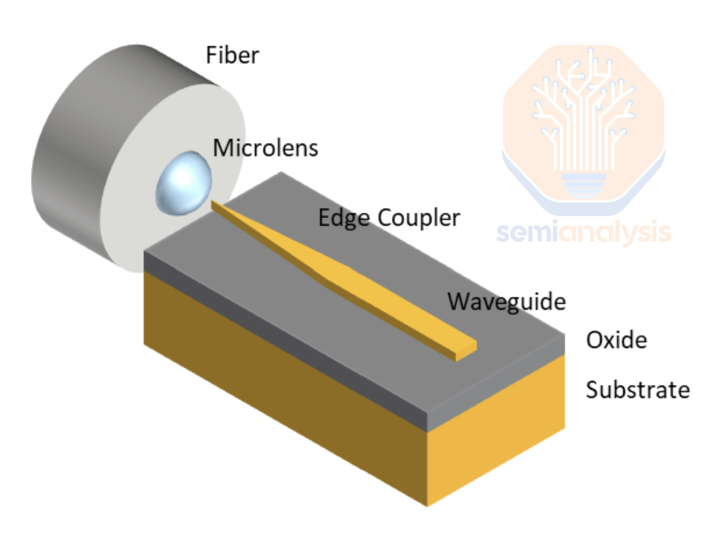 Source: Ansys
Edge coupling is favored for its low coupling loss, ability to work with a wide range of wavelengths, and polarization insensitivity. However, it also comes with a few disadvantages:
- The fabrication process is more complex, and requires undercut and deep etching;
- Fiber density can be limited because it’s a 1D structure;
- It is incompatible with die stacking (as TSV needs thinning);
- Challenges on mechanics reliability on form factor, mechanical stress, warpage, and fiber handling;
- It offers less thermal reliability; and
- There is a lack of ecosystem compatibility in general.
Global Foundries (GFS) demonstrated a monolithically integrated SiN edge coupler that enables 32 channels and 127µm-pitches on its signature 45nm “Fotonix” platform at this year’s VLSI conference.
Grating Coupling (GC)
In grating couplers (GCs), light enters from the top and the fiber is positioned at a small angle above the grating. As the light reaches the grating, the periodic structure scatters and bends the light downward into the waveguides.
The major benefit of grating/vertical coupling is the ability to have multiple rows of fibers, allowing more fibers per optical engine. GCs also do not need to be placed at the bottom of the substrate, making it possible to place the OE on the interposer. Lastly, GC does not need to be positioned with extreme precision and it can be more easily manufactured with a simple two-step etched process. The drawbacks of GC is that single-polarization grating couplers only work for a limited range of wavelengths and are highly polarization sensitive.
Nvidia had a preference for GC due to its several advantages – it enables 2D density, offers a smaller footprint, is easier to manufacture, and allows for simpler wafer-level testing compared to EC. However, the company is also aware of GC’s several drawbacks – it generally introduces higher optical loss and has a narrower optical bandwidth than EC (the latter can generally accommodate a broader spectral range).
TSMC also clearly has a higher preference for GC, which is supported in their COUPE platform.
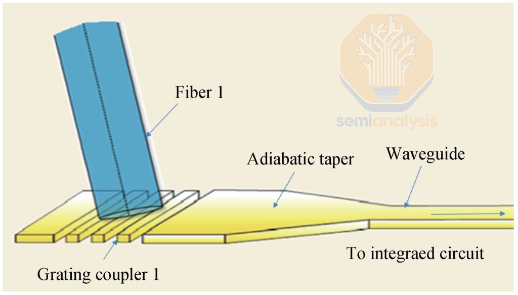 Source: Journal of Semiconductors
Laser Type and Wavelength Division Multiplexing (WDM)
There are two main ways to integrate lasers into CPO.
The first approach, on-chip lasers, integrates the laser and modulator on the same photonic chip, typically by bonding III‑V (InP) materials onto silicon. While on-chip lasers simplify design and reduce insertion loss, there can be a few challenges:
- Lasers are known to be the one of the most failure prone components within the system – failures would have a high blast radius if integrated into the CPO engine as it would take down the whole chip;
- Lasers are also sensitive to heat, placing them on a co-packaged OE would expose a laser to high heat as it would be very close to the hottest part of the system, the host silicon, which would only exacerbate the issue;
- On-chip lasers typically struggle to deliver high enough power output.
The one approach where the industry has come to a consensus is to use an External Light Sources (ELS). The laser is in a separate module connected to the optical engine via fiber. Often times, this laser is in a pluggable form factor like OSFP. This setup simplifies field servicing in the fairly common case of laser failures.
The downside of the ELS is higher power consumption. As seen in the diagram below, in an ELS based system, output power is lost at multiple stages due to various factors like connector losses, fiber coupling losses and modulator inefficiencies. As such, each laser in this system must provide 24.5 dBm of optical power to compensate for losses and ensure reliable transmission. High-output lasers generate more heat and degrade faster under thermal stress, with lasers and thermo-electric coolers accounting for ~70% of ELS power consumption. While incremental improvements in laser design, packaging, and optical paths help, the issue of high power requirements of lasers has not been fully solved.
At this year’s VLSI conference, Nvidia highlighted several laser partners within its ecosystem: Lumentum for single high-power DFBs, Ayar Labs for DFB arrays, Innolume for quantum-dot mode-locked combs, and Xscape, Enlightra, and Iloomina for pumped nonlinear resonant combs.
Nvidia has also discussed exploring VCSEL arrays as a potential alternative laser solution. While the per-fiber data rate would be lower and there may be some thermal issues, VCSELs may offer power and cost efficiency and can be suitable for “wide-and-slow” applications. That said, we don’t see this as an immediate priority for Nvidia.
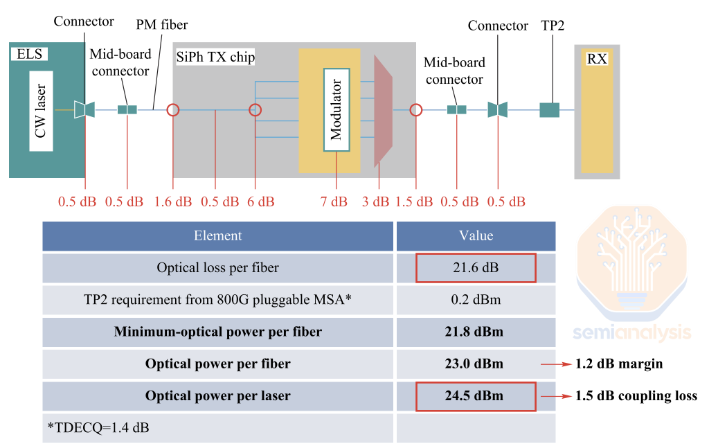 Source: CPO status, challenges, and solutions
Wavelength Division Multiplexing (WDM) is when multiple different wavelengths, or lambdas, of light are transmitted over the same strand of fiber. The two common variants of WDM are Coarse WDM (CWDM) and Dense WDM (DWDM). CWDM typically carries fewer channels spaced relatively far apart (typically 20 nm spacing), while DWDM packs many lanes with very tight spacing (often <1nm spacing). CWDM’s wider channel spacing limits its capacity, while DWDM’s narrower spacing can accommodate 40, 80, or even more than 100 channels. WDM is important because most implementations of CPO proposed today are limited by the number fibers that can be attached to the optical engines. Limited fiber pairs means each fiber pair must be maximized.
Modulator Types
When the lasers enter the PIC, they undergo a modulation phase (driven by drivers) where electronic signals are encoded into laser’s wavelength. The three primary types of modulators used for this process are Mach-Zender Modulators (MZMs), Micro-Ring Modulators (MRMs), and Electro-Absorption Modulators (EAMs). Each individual lambda (individual wavelength on an individual optical lane) requires one modulator.
Mach-Zehnder Modulator (MZM)
MZM encodes data by splitting a continuous-wave optical signal into two waveguide arms whose refractive indices are varied by an applied voltage. When the arms recombine, their interference pattern modulates the signal’s intensity or phase.
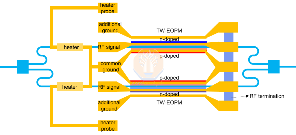 Source: Luceda Academy
MZMs are the easiest of the three to implement and have low thermal sensitivity, reducing the need for precise temperature control. Their high linearity supports advanced modulation formats like PAM4 and coherent QAM (although QAM is not suitable for HPC/AI workloads). MZM’s Low chirp improves signal integrity for higher-order modulation and long-distance transmission. MZMs also enable higher bandwidth per channel: 200G per lane has been proven working, and 400G per lane is believed possible with non-coherent PAM modulation.
However, MZM’s drawbacks are:
- Large form factor with dimensions measured in millimeter scale for **length** (compared to MRM in micron scale), since they require two waveguide arms and a combining region, consuming more chip area and limiting the density of modulators (and thus channels) contained in an OE PIC. MZM sizes are on the order of ~12,000µm², GeSi EAMs at around 250µm² (5x50µm) with MRMs at between 25µm² and 225µm² (5-15µm² in diameter). This is one critical drawback of MZMs that can limit scaling. However, if one considers the size of a full PIC/EIC combination, including drivers and optical/ electrical control circuitry around the modulators, MZMs size disadvantage could appear less notable,
- High power consumption, as the phase-shifting process demands significant energy. It also has higher bias conditions – basically initiating voltages – than MRM (which operates at sub-voltage). However, firms like Nubis are trying to develop clever designs to ameliorate the power disadvantages of MZMs.
In the startup ecosystem, Nubis is one of the firms that mainly utilize MZM for their scale-up CPO solutions. MZMs are not widely selected in the startup ecosystem due to its large form factor and limited number of lambdas.
Micro-Ring Modulators (MRMs)
MRM uses a compact ring waveguide coupled to one or more straight waveguides. An electrical signal alters the ring’s refractive index, shifting its resonant wavelength. By tuning resonance to align or misalign with the input light, MRMs modulate the optical signal’s intensity or phase, thereby encoding data.
A light source is passed into the ring from the input port – for most wavelengths of light, there will be no resonance in the ring such that the light will pass through the device, from the input port to the through port. If the wavelength satisfies the resonance condition, then light will constructively interfere in the ring, and will be instead pulled into the drop port. As illustrated in the normalized power graph below, light of a specific wavelength will cause a sharp peak in transmission power at the drop port and a corresponding drop in transmission at the through port. This effect can be used for modulation.
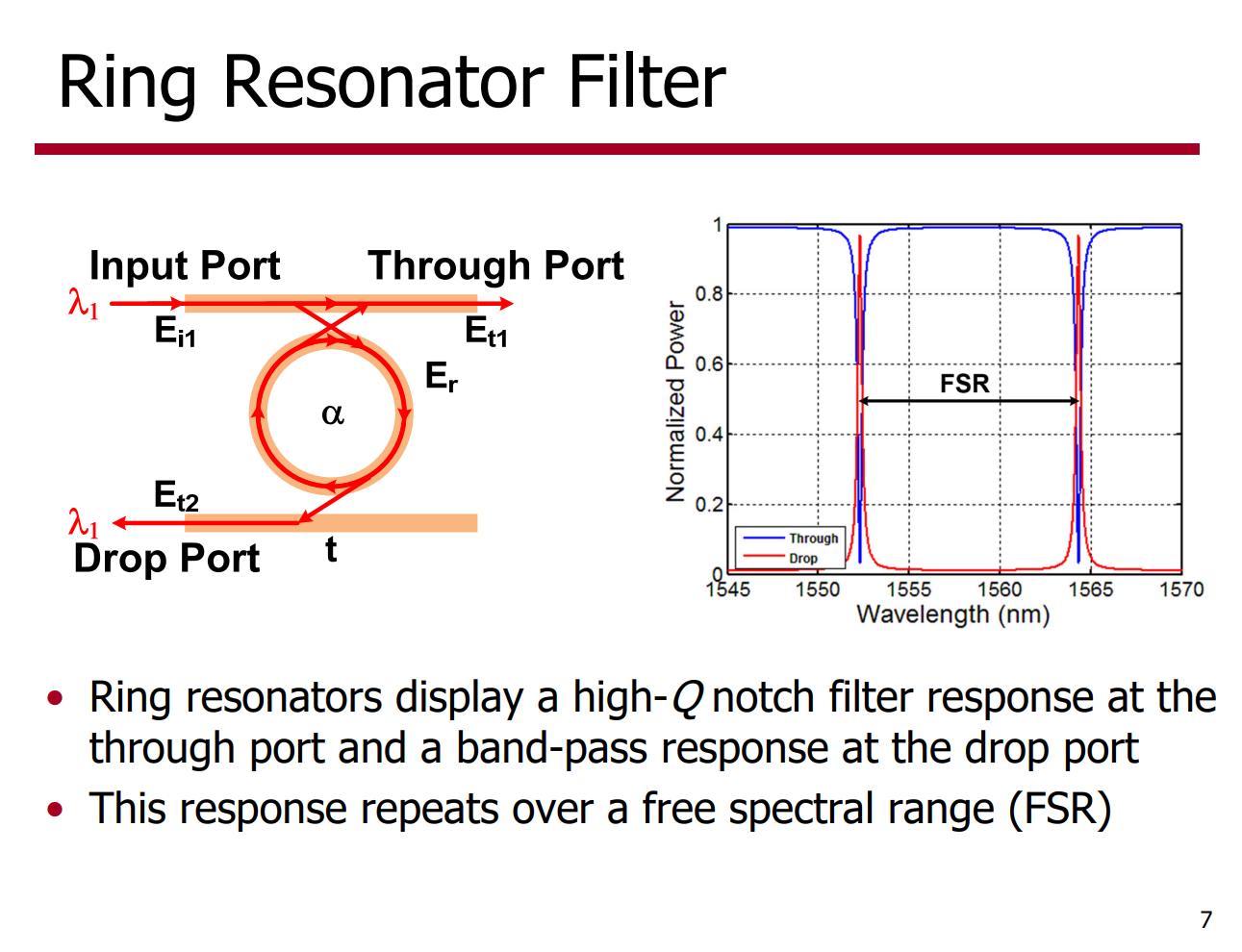 Source: Sam Palermo, Texas A&M University
Optical Engines typically use multiple MRMs, and each of these rings can be tuned to a different wavelength, enabling wavelength division multiplexing (WDM) using the rings themselves as opposed to requiring an additional set of devices to accomplish WDM.
MRMs have a few key advantages:
- The are extremely compact (scale in the tens of microns), allowing far higher modulator density than MZMs. MZM sizes are on the order of ~12,000µm2, GeSi EAMs at around 250µm2 (5x50µm) with MRMs at between 25µm2 and 225µm2 (5-15µm2 in diameter);
- Rings are very well-suited for WDM applications (including DWDM with 8 or 16 wavelengths), and built-in mux/demux functionality;
- MRMs can be highly energy efficient (lower power per bit);
- And finally - rings have low chirp, which improves signal quality.
However, MRMs also come with a few challenges:
- MRMs can be 10-100 times more temperature-sensitive than MZMs and EAMs, requiring very precise control systems that are challenging to design and manufacture;
- They are non-linear, complicating higher-order modulation like PAM4/6/8;
- MRMs’ sensitivity and tight temperature control tolerances can make standardization difficult, since each design has precise requirements.
Among the solution providers, Nvidia has a clear preference for MRMs. They claimed to be the first to design and put MRMs in CPO systems. The company believes MRM’s key advantages are its compact size and low driving voltage, which helps reduce power consumption. However, MRM technology is also known to be difficult to control, making design precision crucial for successful implementation – which is indeed an strength of Nvidia.
In terms of fabrication, TSMC’s advanced CMOS expertise is well suited for fabricating MRMs with high-precision and great Q-factor. In addition, Tower also bring strong fabrication capabilities to their photonics nodes.
MRMs are challenging to implement but is certainly feasible. They can potentially enable higher bandwidth densities than MZMs. That’s why TSMC, Nvidia, and many CPO companies such as Ayar Labs, Lightmatter, and Ranovus, focus on this technology roadmap.
Electro-Absorption Modulators (EAM)
EAMs modulate signals by altering their ability to absorb light based on the voltage applied. More specifically, when low or no voltage is applied to an EAM, the device allows most of the incoming laser light to pass through, making it appear transparent or “open.” When a higher voltage is applied, the band gap of a GeSi modulator shifts to cover the high C-band range (above 1500nm), increasing the absorption coefficient for those wavelengths and attenuating “closing” the optical signal that is passing through the nearby waveguide. This is known as the Franz-Keldysh effect. This switching between “open” and “close” states modulates the intensity of the light, effectively encoding data onto the optical signal.
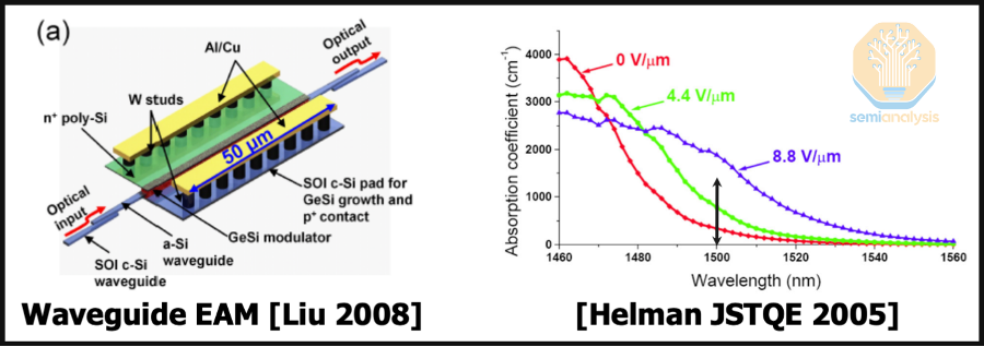 Source: Texas A&M University, Liu 2008, Helman 2005
The same principle is used today in transceivers that use Electro-Absorption Modulated Lasers (EMLs) for modulation. A continuous wave (CW) distributed feedback (DFB) lasers and an InP based EAM is coupled together to build up a single discrete EML, which can modulate one lane. For example, an 800G DR8 transceiver uses 8 EMLs across 8 individual fiber lanes, each using PAM4 modulation (2 bits/signal) and signaling at ~56 GBaud. Unlike GeSi based modulators, the band gap of an InP modulator corresponds to the O-band (1310nm) which is the standard wavelength used is all Datacom DR optics, allowing a great degree of interoperability.
InP modulators have a few downsides that make it less than ideal for use in CPO. InP wafers tend to be small (3” or 6”) and suffer from low yields – both factors drive up unit costs for InP-based devices when compared to Silicon which can be built on 8” or 12” processes. Coupling InP to Silicon is also far more difficult than coupling GeSi to other silicon devices.
EAMs have several advantages compared to MRMs and MZIs:
- Clearly – both EAMs and MRMs have control logic and heaters that act to stabilize both against variations in temperatures, but EAMs have fundamentally less sensitivity to temperature. Compared to MRMs, EAMs have much better thermal stability above 50° C while MRMs are very sensitive to temperature. A typical stability of 70-90 pm/C for MRMs mean that a 2° C variation shifts resonance by 0.14nm, well beyond the 0.1nm resonance shift at which MRM performance collapses. In contrast, EAMs can tolerate an instantaneous temperature shift of up to 35° C. This tolerance is important in particular for Celestial AI’s approach as their EAM modulator resides within an interposer beneath a high-XPU power compute engine that dissipates hundreds of watts of power. EAMs can also tolerate high ambient temperature ranges of around 80° C which may be applicable for chiplet applications which sit next to the XPU and not beneath it.
- Compared to MZIs, EAMs are much smaller in size and consume less power as the relatively large size of MZIs requires a high voltage swing, amplifying the SerDes to achieve a swing of 0-5V. Mach Zender Modulators (MZMs) are on the order of ~12,000µm2, GeSi EAMs at around 250µm2 (5x50µm) with MRMs at between 25µm2 and 225µm2 (5-15µm2 in diameter). MZIs also require more power usage for the heaters needed to keep such a large device at the desired bias.
On the other hand, there are a few drawbacks in using GeSi EAMs for CPO:
- Physical modulator structures built on Silicon or Silicon Nitride such as MRMs and MZIs have been perceived to have far greater endurance and reliability than GeSi based devices. Indeed, many worry about the reliability of GeSi based devices given the difficulty of working with and integrating Germanium-based devices, but Celestial argues that GeSi based EAMs, which are essentially the reverse of a Photodetector, are a known quantity when it comes to reliability given the ubiquity of photodetectors in transceivers today.
- GeSi modulators’ band edge is naturally in the C-band (i.e. 1530nm-1565nm). Designing quantum wells to shift this to the O-band (i.e. 1260-1360nm) is a very difficult engineering problem. This means that GeSi based EAMs will likely form part of a book-ended CPO system and cannot easily be used to participate in an open chiplet-based ecosystem.
- Building out a laser ecosystem around C-band laser sources could have diseconomies of scale when compared to using the well-developed ecosystem around O-band CW laser sources. Most datacom lasers are built for the O-band but Celestial points out that there are considerable volumes of 1577nm XGS-PON lasers manufactured. These are typically used for consumer fiber to the home and business connectivity applications.
- A SiGe EAM has an insertion loss of around 4-5dB vs 3-5 dB for both MRMs and MZIs. While MRMs can be used to directly multiplex different wavelengths, EAMs require a separate multiplexer to implement CWDM or DWDM, adding slightly to the potential loss budget.
Overall, EAMs are not widely used in current CPO implementations, with Celestial AI standing out as one of the few companies actively pursuing this approach.
OE roadmap – scaling OEs
The Optical Engines available today typically offer between 1.6T and 3.2T of aggregate bandwidth. Nvidia’s Quantum CPO includes a 1.6T engine, with a 3.2T version planned for Spectrum. Broadcom has shown off their 6.4T OE for Bailly, but the form factor is very big (2-3x the width of Nvidia) and it requires two FAUs so its bandwidth density may be similar to what Nvidia’s offering. This is the same case for Marvell’s 6.4T OE, requiring 2 FAUs, so it occupies a large footprint. Marvell’s OE is not going into any production systems that we know of anytime soon either.
As we’ve discussed, the 3.2T OE implementation in Nvidia’s Spectrum-X photonics switches does not offer more shoreline bandwidth density than pluggables that are driven by long reach SerDes. In other words, optical engine density must scale multiple times to deliver a compelling performance advantage and drive customer adoption. This means scaling both the electrical interface between the host silicon and the OE EIC, as well as scaling the amount of bandwidth coming out of the fibers.
But what if we were able to design the next generation of interconnect with a free hand – what could be approaches for unlocking greater bandwidth for this generation and beyond?
Key approaches for scaling bandwidth
Let’s discuss the key approaches for scaling bandwidth from co-packaged optical engines:
⚠️ 【付费墙】 原文自此进入付费订阅内容(CPO 带宽扩展的具体路径、CPO 专营公司图谱与供应链拆解等),本页不再收录;完整内容请在 SemiAnalysis 原站 订阅阅读。
第二部分:解析(深度解读)
一、核心论点摘要
这篇 SemiAnalysis 的”CPO 之书”是该机构对共封装光学最系统的一次公开梳理,免费部分已覆盖四个层次:
- 为什么是现在:AI 工作负载的网络需求让”这次不一样”。可插拔光模块(pluggable)过去靠性价比和标准化互操作一直压制 CPO,但 AI 互连在速率、距离、密度、可靠性四个维度即将同时超出可插拔的能力边界。
- Scale-up 才是主战场:市场注意力在 scale-out(NVIDIA/Broadcom 的 CPO 交换机),但作者明确判断——CPO 将成为本十年后半段 scale-up 网络带宽增长的主驱动。铜互连(NVLink 7.2→14.4 Tbit/s)距离被锁死在 2 米内、scale-up 域最多一两个机架;CPO 用同样甚至更好的带宽密度换取更大的 scale-up 域。
- 功耗账是核心卖点:可插拔方案里信号要先走 15–30cm 电学通道到前面板,靠 LR SerDes + DSP 恢复信号;CPO 把光引擎贴到 XPU/交换 ASIC 旁边,省掉 DSP、用低功耗 SerDes,传输能耗降 50%+,激进目标是 80%。
- 调制器三分天下:MZM(成熟、线性度好、但毫米级太大、功耗高)、MRM(微米级、天然支持 WDM、能效高,但温漂 10–100 倍、非线性)、EAM(温度容忍度最好、尺寸小,但 GeSi 可靠性与 C-band/O-band 生态错位是硬伤)。NVIDIA 押 MRM,Celestial AI 押 EAM,Nubis 是少数押 MZM 的初创——技术路线选择直接映射公司基因。
二、关键概念解读
| 概念 | 含义 | 投资/技术含义 |
|---|---|---|
| Scale-up vs Scale-out | Scale-up=机架内 GPU 互连(NVLink 域);Scale-out=跨机架网络 | Scale-up 对延迟/带宽密度更敏感,是 CPO 价值密度最高的场景;Celestial AI 预计 2028 年底 $1B 营收主要靠 Amazon Trainium 4 的 scale-up CPO |
| OE(Optical Engine) | 贴装在交换芯片/XPU 旁的光电引擎 | 当前 1.6T–3.2T;NVIDIA Quantum 1.6T→Spectrum 3.2T;Broadcom/Marvell 6.4T 但体积 2–3 倍、需双 FAU,带宽密度未必更高 |
| Shoreline bandwidth density | 芯片边缘每毫米可引出的带宽 | 3.2T OE 对 LR SerDes 驱动的可插拔尚无密度优势——OE 密度必须翻数倍才能驱动客户采用,这是 CPO 渗透率的真正闸门 |
| TSMC COUPE | 台积电硅光封装平台 | MRM 高精度制造依赖先进 CMOS 工艺,TSMC/Tower 的硅光节点是 MRM 路线的制造底座 |
| FAU(Fiber Array Unit) | 光纤阵列耦合单元 | OE 的”最后一毫米”,数量直接决定封装面积与耦合良率,也是本站 CPO 测试系列反复出现的瓶颈环节 |
| Book-ended system | 端到端绑定的封闭系统 | GeSi EAM 天然 C-band,难以融入 O-band 开放 chiplet 生态 → EAM 路线注定做”整柜绑定”生意,与开放生态互斥 |
三、调制器路线对比(全文最有决策价值的部分)
| 维度 | MZM | MRM | EAM (GeSi) |
|---|---|---|---|
| 尺寸 | ~12,000 µm²(毫米级长度) | 25–225 µm² | ~250 µm² |
| 温度敏感性 | 低 | 高(70–90 pm/°C,2°C 即崩溃) | 最好(瞬时 35°C、环境 80°C) |
| WDM 支持 | 需外加 mux/demux | 环本身即 mux/demux,支持 DWDM 8/16λ | 需外加 mux |
| 线性度/高阶调制 | 最好(PAM4/QAM) | 非线性,PAM4+ 困难 | 中等 |
| 插入损耗 | 3–5 dB | 3–5 dB | 4–5 dB |
| 生态/可靠性 | 最成熟 | TSMC/NVIDIA/Ayar/Lightmatter/Ranovus 押注 | Ge 集成可靠性存疑;C-band 激光生态规模不经济 |
| 代表玩家 | Nubis | NVIDIA、Ayar Labs、Lightmatter、Ranovus | Celestial AI |
解读:这不是”谁最优”的学术问题,而是场景匹配问题——Celestial 的 EAM 贴着数百瓦 XPU 的 interposer 下方,只有 EAM 扛得住温度;NVIDIA 有顶级控制设计能力,才敢吃 MRM 的温漂螃蟹。看一家 CPO 公司选什么调制器,基本能反推它的封装位置、目标客户和生态策略。
四、产业信号与趋势判断
- 从”if/why”到”when/how”:CPO 专营公司已越过论文/演示阶段,进入面向量产的端口架构决策;瓶颈从”技术可行性”转向”量产爬坡 + 激光器等供应链产能”。
- Hyperscaler 开始锁定 scale-up CPO 供应商:Amazon(Trainium 4 ↔ Celestial AI/Marvell 收购案)是第一个公开信号,后续 Microsoft/Google/Meta 的站队将决定初创梯队座次。
- OE 带宽密度是下一个军备竞赛指标:1.6T→3.2T→6.4T 的演进必须伴随 FAU/封装密度同步,否则只是”更宽的引擎、同样的海岸线”。
- 激光器供应链是被低估的卡点:C-band vs O-band 之争(EAM 路线需要 C-band 激光生态)会外溢到激光器厂商的产能规划,XGS-PON 1577nm 产能是 Celestial 现阶段的”曲线救国”依据。
五、与本站其他文章的连接
- 与《Why CPO Is Becoming Inevitable?》互为表里:那篇讲”铜墙”物理瓶颈,本文给 TCO/功耗的量化账。
- 《CPO, Fully Dissected》的封装解剖可与本文的 OE/EIC/PIC 结构对照阅读。
- 调制器之争直接影响测试策略:MRM 的温控标定、EAM 的 C-band 光源,都会落到《CPO 测试市场机会》《Everything You Need to Know About CPO Testing》所讲的晶圆级光测试增量上。
- 《There Is No Such Thing as a “CPO Stock”》提醒:本文列出的供应链玩家(NVIDIA/Broadcom/Marvell/TSMC)CPO 营收占比都极小,别把本文的技术结论直接映射成”纯 CPO 标的”。
六、风险提示
- 免费段不完整:本文最有投资含金量的部分(带宽扩展路径、CPO 专营公司图谱、供应链拆解)在付费墙后,以上解读仅基于免费段,结论可能片面。
- 路线锁定风险:MRM/EAM/MZM 之争尚无终局,押错路线的初创(以及为其配套的激光器/测试供应商)存在被整体绕开的风险。
- 量产时点风险:CPO 历史上多次”狼来了”,3.2T OE 相对可插拔尚无海岸线密度优势意味着可插拔+LPO/NPO 的生命周期可能比多头预期更长。
- 单一信源风险:SemiAnalysis 与产业链玩家存在业务往来,其供应链判断建议与 TrendForce、LightCounting 等独立数据交叉验证。
以上解读基于原文免费公开部分整理,不构成投资建议。