Why CPO Is Becoming Inevitable? [CPO Special Part 1] — 为什么 CPO 正变得不可避免
本文为 Damnang 关于 CPO(共封装光学)系列第一篇的英文原文,系统梳理数据中心 GPU 互连的距离分层、铜互连的『铜墙』瓶颈,以及交换 ASIC 到前面板光模块之间 15–30cm 电学通道的功耗、空间与可靠性问题,并详解 CPO 如何用『毫米级』封装把电学距离压到极致、省掉 DSP、带来 50–80% 的功耗下降。附中文深度解读。
本文整理自 Damnang(Substack),原文发布于 Mar 19, 2026(标题原文:Why CPO Is Becoming Inevitable? [CPO Special Part 1])。 结构为 正文(英文原文)+ 解析(中文深度解读),方便中英对照阅读。 来源说明:内容经公开页面获取;本发布保留完整英文原文并附中文深度解读,仅作信息整理与学习用途,著作权归原作者所有,建议在原站支持作者订阅。 原文链接:damnang2.substack.com
第一部分:正文(Original Article)
Why CPO Is Becoming Inevitable? [CPO Special Part 1]
Damnang · Mar 19, 2026
1. What Does a Data Center Look Like?
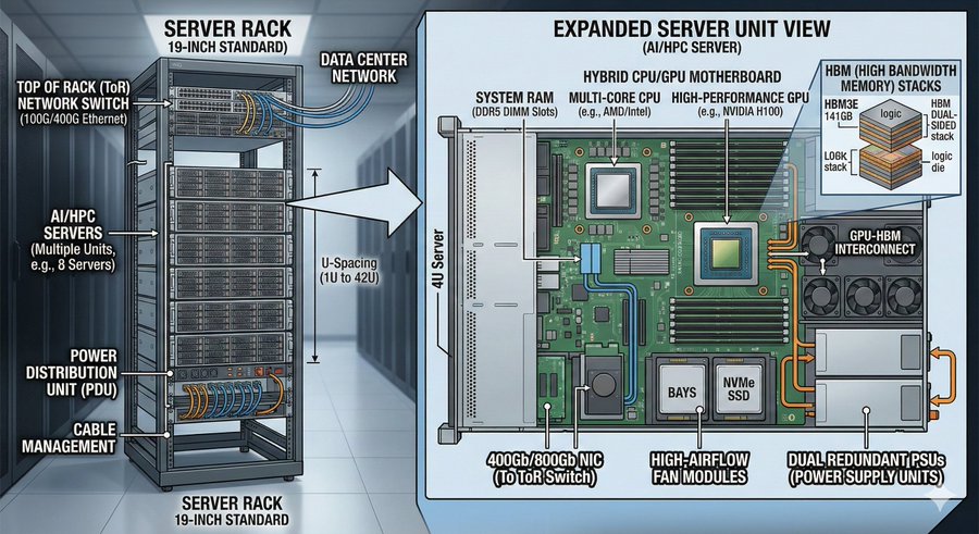
To train AI, thousands to tens of thousands of GPU chips must run simultaneously. These GPUs don’t work alone — they constantly exchange data with each other in a collaborative process. A data center is simply where all these GPUs live together.
It’s easy to picture a data center as one giant computer, but in reality it’s built by stacking small, repeating units. That basic unit is called a rack.
A rack is a metal cabinet-style frame, roughly two meters tall, with multiple servers slotted vertically inside. Think of a server as a computer housing several GPU cards — typically four, eight, or sometimes dozens per server, alongside CPUs, memory, and storage.
Racks don’t just hold servers, though. Network switches live in there too. A switch is essentially a traffic controller: it collects data from the servers in the rack, organizes it, and sends it outward. Because switches usually sit at the top of the rack, they’re called ToR (Top of Rack) switches.
Multiple racks line up in a row, and multiple rows come together to form a section of the data center. The reason for this structure is straightforward — power distribution, cooling, cable management, and maintenance are all standardized at the rack level. Even the most powerful AI systems ultimately sit on top of this same rack-based foundation.
2. How Does Data Move? Inside the Rack and Beyond
Having tens of thousands of GPUs means nothing if they can’t talk to each other. GPU communication generally breaks down into two segments, and because the distances differ, so do the methods.
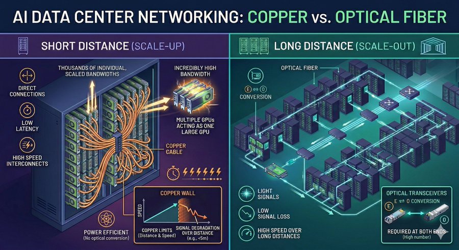
Short distances (Scale-up Network): Where copper has the advantage
For short runs — within a single rack or between adjacent racks — sending electrical signals over copper cable is the practical choice.
When GPUs within the same rack communicate, they use dedicated high-bandwidth interconnect technology that links dozens of GPUs directly to one another. The speeds involved are in the hundreds of GB/s to TB/s range per GPU, effectively turning a cluster of GPUs into one massive processor. This is called the scale-up network.
The same logic applies to GPU-to-switch connections inside the rack. Cables here typically run two to three meters, and copper handles that just fine. At today’s 800G speeds, passive copper cables (DAC) can reach around three meters, while active copper cables (AEC) stretch to about five.
Copper’s advantages are clear: simpler components, no expensive optical conversion hardware, easier maintenance, and better power efficiency at short distances.
That said, copper feels the strain as speeds climb. High-speed electrical signals degrade and distort as they travel through cables, connectors, and circuit board traces. The faster the signal, the worse the degradation, and the more complex the correction circuitry needed to compensate — which means more power and more heat. What once worked with any copper cable now demands tight tolerances on cable quality, connector precision, and compensation circuits. The usable distance for copper keeps shrinking as speeds rise. This is what the industry calls the “Copper Wall.”
Long distances (Scale-out Network): Where fiber becomes essential
Longer runs change everything. Once you’re spanning more than a few meters — crossing between racks in the same row, connecting racks across the hall, or stretching hundreds of meters across a data center floor — copper simply can’t do it. Optical fiber is the standard.
Training large AI models requires thousands to tens of thousands of GPUs, which means dozens to hundreds of racks need to be interconnected. This is the scale-out network, also called the backend network. Each GPU has a network interface card (NIC) that connects to a switch, and those switches connect upward to higher-level switches, eventually forming a fabric where any GPU can reach any other GPU. A large portion of these scale-out connections run over optical fiber.
Fiber’s strength is distance. Light travels long runs with almost no signal loss, and higher speeds don’t shrink the reach the way they do with copper. The cables themselves are also thin and lightweight, which makes routing and cable management much more manageable.
There’s one added step with fiber, though. Since GPUs and switches operate on electrical signals, the signal has to be converted to light before transmission and converted back to electricity upon arrival. The device that handles this conversion is an optical transceiver, commonly called an optical module. One sits at each end of every connection. In a data center with hundreds of thousands of GPUs, that adds up to millions of optical modules.
The bottom line: short distances (within a few meters) use copper, long distances (tens of meters and beyond) use light. In between, either can work depending on speed and conditions, but the range where copper holds up keeps narrowing as speeds increase. That’s the operating principle behind today’s data centers.
3. The Actual Path Data Takes
Section 2 laid out the big picture: copper for short runs, light for long ones. Now let’s trace the actual path data follows step by step, because understanding this path is what makes the bottlenecks visible — and explains why CPO matters.
Scale-up: GPU-to-GPU communication within the same rack
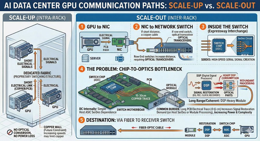
The path for two GPUs in the same rack talking to each other is relatively simple:
GPU → copper cable → switch chip → copper cable → GPU
Distances are short, so the whole thing runs on electrical signals, handled by copper cables or board traces. There’s no need to convert anything to light, so no optical modules, and none of the power losses that come with electrical-to-optical conversion.
That said, this segment won’t stay copper-only forever. As bandwidth keeps growing, the distance electrical links can reliably cover keeps shrinking, putting more pressure on cables, connectors, and compensation circuits. Eventually this segment will hit copper’s limits too — more on that later.
Scale-out: Communicating with a GPU in a different rack
When a GPU needs to send data to one in another rack, the path becomes considerably more involved.
Step 1: GPU to NIC
Data generated by the GPU first goes to the network interface card (NIC) in the same server. This is a short internal path handled entirely by board traces, so electrical signals are fine.
Step 2: NIC to network switch
The electrical signal leaves the NIC and travels via cable to the network switch. Whether this uses copper or fiber depends on distance and physical layout. If the switch sits at the top of the same rack, copper usually works. But if the switch is located elsewhere — which is increasingly the case in newer data center designs — this segment may already require optical connections.
Step 3: Inside the switch
At the heart of the switch is a specialized chip called a switch ASIC. Think of it as the interchange on a highway — it takes incoming data and routes it toward the right destination.
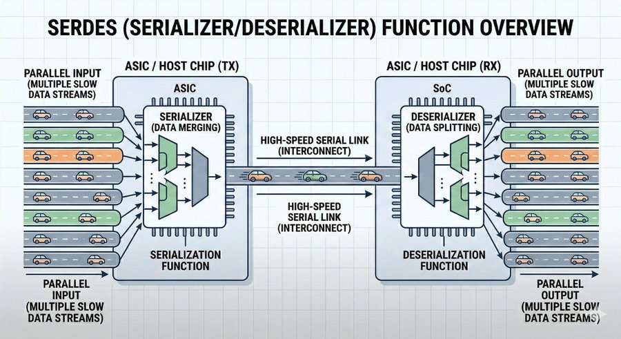
Inside the switch ASIC is a circuit called SerDes. SerDes takes the chip’s internal data and converts it into a high-speed serial signal to send outward — similar to merging multiple lanes of traffic into a single fast highway lane.
Step 4 (Problematic one): Switch ASIC to front-panel optical module
The high-speed electrical signal coming out of the switch ASIC doesn’t get converted to light immediately. Instead, it travels across the switch’s circuit board — roughly 15 to 30 centimeters — before reaching the optical module plugged into the front panel.
That “15 to 30 centimeter electrical stretch” is where problems pile up. High-speed signals degrade and distort even across short distances, so before or inside the optical module, the signal has to be cleaned up.
For those less familiar with the technical details, here’s a simplified way to think about it as one bundled process:
Signal conditioning (DSP): Restores distorted waveforms to a readable state.
Clock recovery: Re-establishes the timing reference for when to sample the signal.
Retiming: If needed, regenerates the signal from scratch.
Forward Error Correction (FEC): Catches and fixes bit errors on the receiving end.
As distances grow and speeds increase, this “signal rescue” operation has to work harder and grow more complex. The conclusion is straightforward: the farther the signal has to travel electrically before becoming light, the more processing and correction it requires, and the more power and design complexity that demands.
Step 5: Fiber to the destinationLight travels through fiber to the switch on the other end. There, an optical module converts it back to an electrical signal, the switch routes it to the right destination, a cable carries it to the target server’s NIC, and finally the data arrives at the GPU.
The segment worth keeping in mind from all of this is Step 4 — the stretch of electrical signal traveling from the switch ASIC to the front-panel optical module across the circuit board. The longer that stretch, the heavier the correction burden and the higher the power consumption. Hold onto that picture, because the next section explains why that segment is such a serious problem — and how CPO changes it.
4. Why CPO Is Needed, and What It Changes
The core problem: The conversion point is too far away
Recall Step 4 from above. In the scale-out path, the electrical signal from the switch ASIC’s SerDes travels 15 to 30 centimeters across the circuit board before reaching the front-panel optical module. That 15 to 30 centimeters produces three specific consequences.
Power is wasted on a significant scale: the DSP inside a single optical module consumes roughly half the module’s total power, and across a large data center, optical modules collectively draw several megawatts. The front panel runs out of physical space: starting with the 102.4 Tbps generation, there simply isn’t enough room for all the ports. And millions of individual components each generate heat and each represent a potential failure point.
The scale-up side isn’t safe either. Copper works fine today, but double or quadruple the speeds and the Copper Wall becomes unavoidable. Extending GPU-to-GPU high-speed direct connections beyond a single rack already makes copper impossible — light becomes the only option.
Scale-out or scale-up, both paths point to the same underlying problem:
The electrical signal is traveling too far.
CPO: Co-Packaged Optics
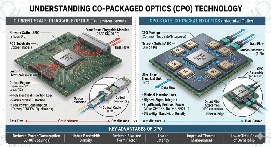
CPO (Co-Packaged Optics) attacks that distance directly. Rather than plugging optical modules into the front panel, it integrates the optical engine — the component responsible for converting electricity to light — into the same package as the switch chip.
The path comparison makes the difference obvious:
Before CPO: chip → (15–30 cm of board traces) → front-panel optical module → fiber
With CPO: chip → (a few millimeters) → in-package optical engine → fiber
The electrical distance drops from 15 to 30 centimeters to just a few millimeters. That single change sets off a chain reaction that reshapes everything else.
The SerDes changes. Previously, sending signals across 15 to 30 cm required powerful long-reach (LR) SerDes with complex equalization circuits and high power draw. With CPO, signals only travel a few millimeters, so low-power extremely short reach (XSR) SerDes is sufficient. Simple correction circuits are enough to maintain signal quality, and this alone cuts power meaningfully.
The DSP shrinks or disappears entirely. In conventional optical modules, the DSP consumed roughly half the module’s power because signals arriving after a 15 to 30 cm journey were heavily degraded. After just a few millimeters in a CPO setup, the signal arrives nearly intact. The DSP can be eliminated completely (DSP-free) or stripped down to just forward error correction (FEC-only, or DSP-lite). This is the single largest source of power savings in CPO.
The front-panel constraint disappears. With optical modules no longer occupying front-panel slots, port count is no longer limited by panel surface area. The same switch can expose significantly more ports.
Component count drops. Instead of dozens of independent optical modules, a few integrated optical engines handle everything in the switch package. Fewer failure points, higher system reliability.
The net result is 50 to 80 percent lower power consumption, with higher bandwidth and more ports from the same switch.
Where things go from here
CPO is being deployed first in scale-out network switches, because that’s where the bottleneck is most acute right now.
The next step is CPO at the NIC level. As noted earlier, newer AI data center architectures are moving switches out of individual racks, which means the NIC-to-switch connection increasingly requires optical modules too. Integrating optical engines into NICs would reduce power consumption and component count in this segment as well.
第二部分:解析(深度解读)
一、这篇文章为什么重要
这是 Damnang 关于 CPO(Co-Packaged Optics,共封装光学)系列的第一篇,定位是「科普 + 第一性原理拆解」,价值在于它把 CPO 的必要性讲清楚了——不是因为某家厂商在推新概念,而是因为 电信号在板级PCB上走的 15–30 厘米距离,正在被 800G/1.6T 速率下的损耗、功耗和前面板空间逼到墙角。
对中文读者(尤其是半导体/算力产业链投资者)而言,这篇文章的重要性有三点:
- 它给出了 CPO 的物理锚点。很多讨论停留在「CPO 能省功耗」的结论层,而本文把它还原成一条具体的信号路径:GPU → NIC → 交换 ASIC(SerDes)→ 板级 15–30cm 电走线 → 前面板光模块 → 光纤。问题就出在第四步那一段「明明是芯片内部高速信号,却要先在电路板上跑二三十厘米才变成光」的浪费。
- 它把「铜墙(Copper Wall)」和「CPO」串成同一条主线。短距(scale-up)的铜互连和长距(scale-out)的光互连,最终都指向同一个根因——电走得太远了。这让读者理解为什么 CPO 不是孤立的「光模块替代方案」,而是 AI 集群从机架内向机架间、从铜向光全面迁移的必然结果。
- 它提供了可量化的判断标尺:DSP 约占单个光模块功耗的一半、整机房光模块合计数兆瓦(MW)级、102.4Tbps 交换芯片代际前面板空间已不够用、CPO 带来 50–80% 功耗下降。这些数字可直接作为后续跟踪产业落地的「验证指标」。
二、核心论点拆解
文章的核心论证链可以压缩成下面这张表:
| 维度 | 传统可插拔光模块(Pluggable) | CPO(共封装光学) | 带来的改变 |
|---|---|---|---|
| 电学距离(ASIC→光) | 15–30 cm 板级走线 | 数毫米(in-package) | 信号几乎不失真,无需重补偿 |
| SerDes 类型 | 长距 LR SerDes(复杂均衡、高功耗) | 极短距 XSR SerDes(简单校正) | 功耗显著下降 |
| DSP | 必需,约占模块功耗一半 | 可全去掉(DSP-free)或仅留 FEC(DSP-lite/FEC-only) | CPO 最大单一节能源头 |
| 前面板空间 | 受端口数限制(102.4T 代际已不够) | 光引擎进封装,不占前面板 | 同芯片可暴露更多端口 |
| 器件数量 | 数十个独立模块、百万级失效点 | 少量集成光引擎 | 失效点减少、可靠性提升 |
| 综合结果 | — | 50–80% 功耗下降 + 更高带宽/端口 | — |
一句话总结文章的论点:CPO 的本质不是「把光做进芯片」,而是「把电变光的位置从前面板挪到封装内几毫米处」,这一个物理距离的改变引发 SerDes、DSP、空间、可靠性的连锁重构。 这是理解整个 CPO/硅光产业逻辑的钥匙。
三、关键概念 / 技术解读
1. Scale-up 与 Scale-out 网络
- Scale-up(纵向扩展):同一机架内 GPU 之间的直接高速互连,目标是把几十张 GPU「拼成一台巨型处理器」,带宽在数百 GB/s 到 TB/s/卡 量级,今天仍由铜缆(DAC/AEC)承载。
- Scale-out(横向扩展/后端网络):跨机架、跨机房把成千上万张 GPU 连成 fabric,距离从几米到数百米,必须上光纤。两者共同构成 AI 训练集群的通信骨架。
2. 铜墙(Copper Wall) 原文的关键洞察:高速电信号每经过一段电缆、连接器、PCB 走线都会衰减和失真,速率越高衰减越严重、补偿电路越复杂、功耗和发热越大。结果是铜可用距离随速率提升不断收缩——800G 下无源铜(DAC)约 3 米、有源铜(AEC)约 5 米,再往上就逼近极限。这就是「铜墙」。它意味着 scale-up 今天能用铜,但速率翻两番后必然撞墙,届时连 GPU 间直连也得上光。
3. 交换 ASIC 内的 SerDes 与「信号救援」四件套 SerDes(串行器/解串器)把芯片内部并行数据并成高速串行信号送出。在 15–30cm 板级走线后信号已失真,光模块内必须做:信号调理(DSP) 恢复波形、时钟恢复 重建采样时序、重定时(Retiming) 必要时重生信号、前向纠错(FEC) 抓错改错。距离越远、速率越高,这套「救援」越重、越费电——这正是 CPO 想消除的负担。
4. DSP 为何是 CPO 的「头号猎物」 传统可插拔模块里 DSP 吃掉约一半模块功耗,根因是信号走了 15–30cm 已严重劣化,必须靠强 DSP 拉回来。CPO 把距离压到几毫米,信号近乎完好到达,于是 DSP 可被整体拿掉(DSP-free)或只留 FEC(FEC-only / DSP-lite)。这是 CPO 功耗收益最大的单一来源,也是博通、英伟达等交换芯片厂商力推 CPO 的核心工程动机。
5. In-package 光引擎 vs 前面板模块 CPO 把负责电-光转换的「光引擎」与交换芯片封在同一 package 内,路径从 芯片 → 板级走线 → 前面板模块 → 光纤 变为 芯片 → 数毫米 → 封装内光引擎 → 光纤。代价是封装、散热、可维护性(坏了不能像插拔模块那样热替换)和测试难度大幅上升——这恰是本站其他文章反复强调的落地瓶颈(见下文链接)。
四、与本站其他 CPO / 硅光系列文章的链接
- The Illusion of CPO? [CPO Special · Final]:本系列的「终章」视角,可与这篇 Part 1 对照阅读,看作者如何从「必然性」走到「幻象/现实落差」的反思。
- Optics Primer Part 3: Co-Packaged Optics:更底层的光学入门,补全本文未展开的封装与耦合原理。
- CPO 最大的瓶颈:高良率量产测试:本文点出「器件数量下降、可靠性提升」的红利,但封装内光引擎的可测试性正是量产最大拦路虎,此文专门拆解。
- 硅光链路预算与光学非理想性:解释把光做进封装后,耦合损耗、温漂、非理想性如何吃掉 CPO 的功耗与带宽红利,是理解「为什么 CPO 没那么容易」的必读。
(另可延伸:CPO/NPO 的激光源 Part 1:InP 与 Part 2:Lumentum 的技术与护城河,看 CPO 封装内光引擎的「光从哪来」;以及 台积电在 CPO 领先、三星第三 的代工格局。)
五、投资意义
需先说明:原文是一篇原理性/概念性科普,通篇未点名任何具体上市公司或 ticker;其投资含义需结合产业链逻辑外推,以下为基于文中技术论断的映射,不构成投资建议。
- 交换 ASIC / 网络芯片厂商:文中「CPO 先在 scale-out 交换芯片落地,下一步进 NIC」直接利好能把光引擎与交换芯片协同设计的平台型厂商(如 Broadcom、NVIDIA、Marvell 等高速交换/互连龙头)。判断信号是 102.4Tbps 代际前面板空间是否真的「不够用」、以及谁率先量产 CPO 交换芯片。
- 硅光 / 光引擎供应商:CPO 把「数十个独立模块」替换为「少量集成光引擎」,利好具备硅光调制器、封装与耦合能力的厂商;同时意味着传统可插拔光模块厂商面临被「封装内集成」替代的份额风险(800G/1.6T 可插拔需求与 CPO 是此消彼长的关系)。
- 激光器(光源)环节:封装内光引擎仍需光源,InP 激光器在外置/可插拔激光源(ELS)方案中价值量提升,对应 Lumentum 等激光供应商的逻辑(见上方激光系列链接)。
- 测试与设备:当光引擎从「可热插拔模块」变成「封装内不可热替换器件」,良率与可测试性成为量产门槛,利好高端光通信测试设备与先进封装/CoWoS 类产能。
- 铜互连的「退守」边界:铜墙意味着 DAC/AEC 在超高速率下距离收缩,但中短距仍长期有成本优势——铜缆/连接器厂商的叙事是「速率越高、铜越短」,而非「铜消失」。
跟踪建议:以文中三个标尺作为验证锚——(1)单模块 DSP 功耗占比是否随 CPO 下降;(2)102.4T 交换芯片前面板端口是否出现物理瓶颈;(3)整机房光模块总功耗是否进入「数兆瓦」量级倒逼架构切换。
六、风险提示
- 落地节奏风险:本文描述的是「为什么必然」,但 CPO 封装的散热、可维护性(坏了不能像插拔模块那样换)、良率与测试难度(见本站高良率测试文)都可能使大规模商用晚于市场预期;「必然」不等于「马上」。
- 技术路线竞争风险:除 CPO 外,还有 NPO(近封装光学)、LPO(线性直驱可插拔,去掉 DSP 的折中方案)、以及继续优化可插拔硅光模块等路径。若 LPO/可插拔在 1.6T 代际就能靠去掉 DSP 拿到大部分功耗收益,CPO 的渗透斜率可能放缓。
- 需求侧风险:CPO 的驱动力是 AI 集群规模与速率,若 AI 资本开支周期性回落或训练集群架构变化,scale-out 光互连总量增速不及预期,会直接削弱 CPO 的紧迫性。
- 供应链与标准风险:CPO 涉及交换芯片厂、光引擎厂、激光器厂、封测厂多方协同,标准(如光引擎接口、可插拔光源规范)未完全统一前,存在阵营分裂与重复投资风险。
- 原文局限:本文为系列开篇,侧重原理与必要性,未给出具体厂商、成本模型、量产时间表与实测数据;其「50–80% 功耗下降」为行业区间预期,实际收益随速率、通道数与实现方案差异很大,引用时需注意边界。
以上解读基于原文信息整理,不构成投资建议。