Winway Copackaged Optics (CPO) Talk — WinWay 与共封装光学(CPO)访谈
本文整理自 Substack《Elementary, Dear Watson》Jack Huang 对 WinWay(台湾测试设备厂)CPO 投资者宣讲的逐页解读,保留完整英文原文,并附中文深度解读,聚焦 CPO 供应链、PIC/EIC、耦合器、测试瓶颈与投资意义。
本文整理自 Elementary, Dear Watson(Substack),原文发布于 Jun 05, 2026(标题原文:Winway Copackaged Optics (CPO) Talk)。 结构为 正文(英文原文)+ 解析(中文深度解读),方便中英对照阅读。 来源说明:内容经公开页面获取;本发布保留完整英文原文并附中文深度解读,仅作信息整理与学习用途,著作权归原作者所有,建议在原站支持作者订阅(来源:https://elementarydearwatson.substack.com)。 抓取说明:本文为免费全文,无付费墙;原站前 18 张配图(商周截图 + 开场及 PIC/EIC 示意图之前的幻灯片)已按原站位置嵌入(substackcdn 包装链已解码为 S3 直链并抽查验证可达);PIC 示意图之后的其余幻灯片因当前抓取环境限制(jina 被 Cloudflare 拦截、全文经 API 取回时被截断)暂未取回,待环境恢复后补齐。
第一部分:正文(Original Article)
Winway Copackaged Optics (CPO) Talk
Takeaways about CPO
Introduction
This post will be the first and last free post of this new newsletter Elementary, Dear Watson, which you can thank my dear friend for. As he liked to remind me in our native tongue (一份材料一份話,沒有材料不說話), I only ever speak to matters within my circle of competence and for which I have both firm practical and theoretical understanding. Because of a certain principle, I can’t and won’t refute the words of many readers (whether on the sell side, buy side, or within a copackaged optics company) one by one, at least not for free. Copackaged optics is a highly technical area that requires rare, valuable expertise in understanding the underlying physics, engineering, and economics. Not understanding the fundamentals when investing in copackaged optics will cost you as an executive of Largan (大立光) found out belatedly - oops, it turned out that CPO is a high precision business that requires significant investment and specialized knowhow. Just knowing the fundamentals can be a key competitive advantage!
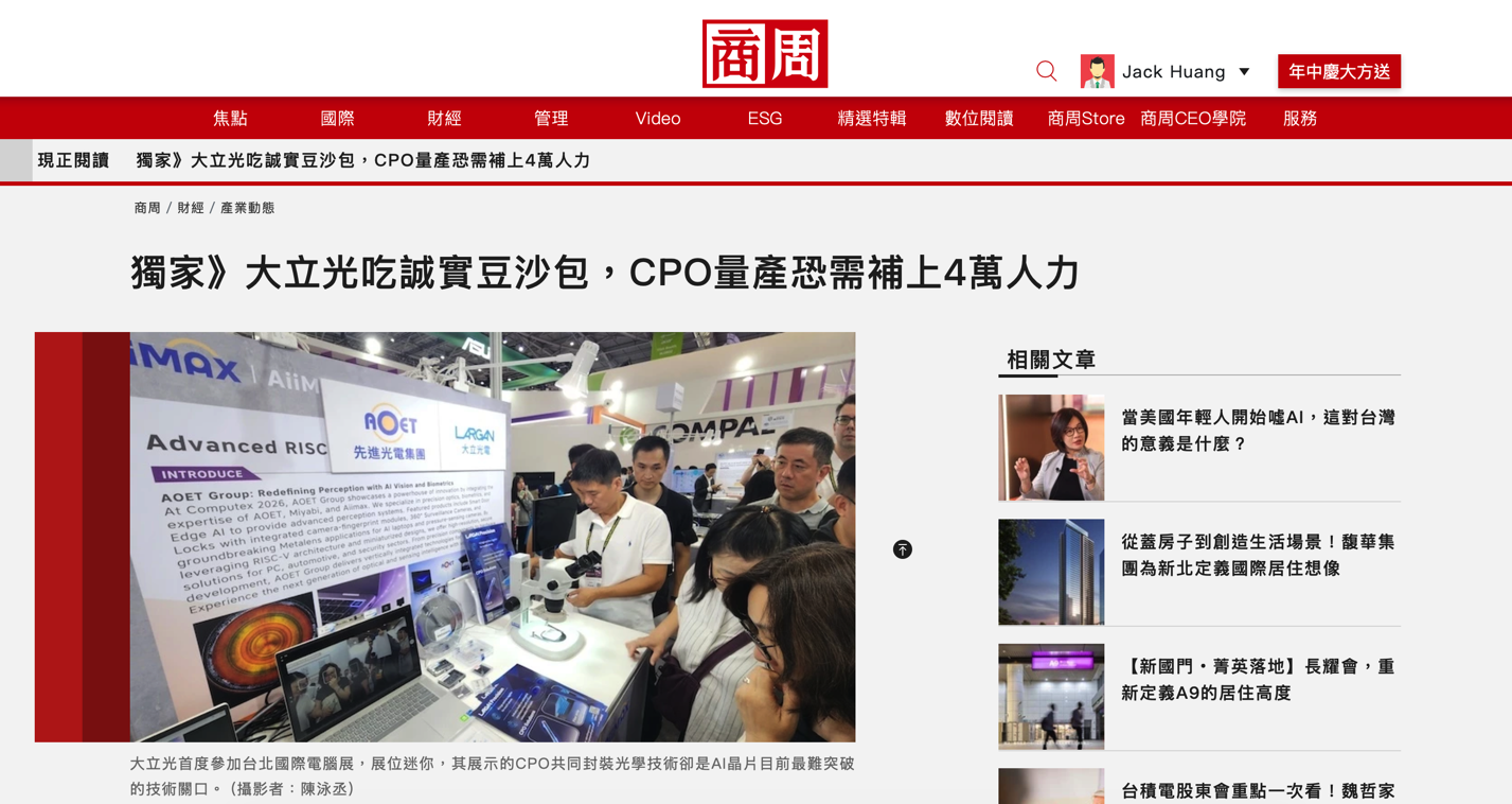
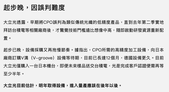
Article title page and relevant passage from this 商周 (local Taiwanese business magazine) piece.
Unique Background
I recognize that I am one of a few Americans who have the technical, financial, and cultural chops to give you a down-to-earth take on different aspects of copackaged optics (CPO), unlike most of the folks opining on the subject. As a Midwesterner, I don’t think pedigree (education/work) matter much in terms of understanding the heart of objective matters, but I did study physics and mathematics in a small liberal art college of sorts in my small Midwestern hometown and work on electronic-photonic design automation software at an EDA company, if that counts for anything. Specifically, I am a Germanophile (many high precision optics and glass vendors are Mittelstand/Nebenwerte companies based in DACH countries) and of Cantonese heritage, so neither Taiwanese or mainland Chinese. My beloved Hong Kong is a non-player in semiconductors except for a small presence of ASMPT (another player worth paying attention to for its small but growing exposure to CPO) in New Territories (香港新界青衣). I will be in the Bay Area this weekend - specifically, South Bay (Palo Alto, San Jose, Santa Clara, etc.) on this Saturday 6/6 and San Francisco on this Sunday 6/7 (feel free to DM me for coffee or something if like minded readers are in the area). As an aside, I recommend reading Fabian, Damnang, PhotonCap, Chad, PhotonEra, Latent Value on Substack for more in depth pieces in this area.
Winway Copackaged Optics Talk
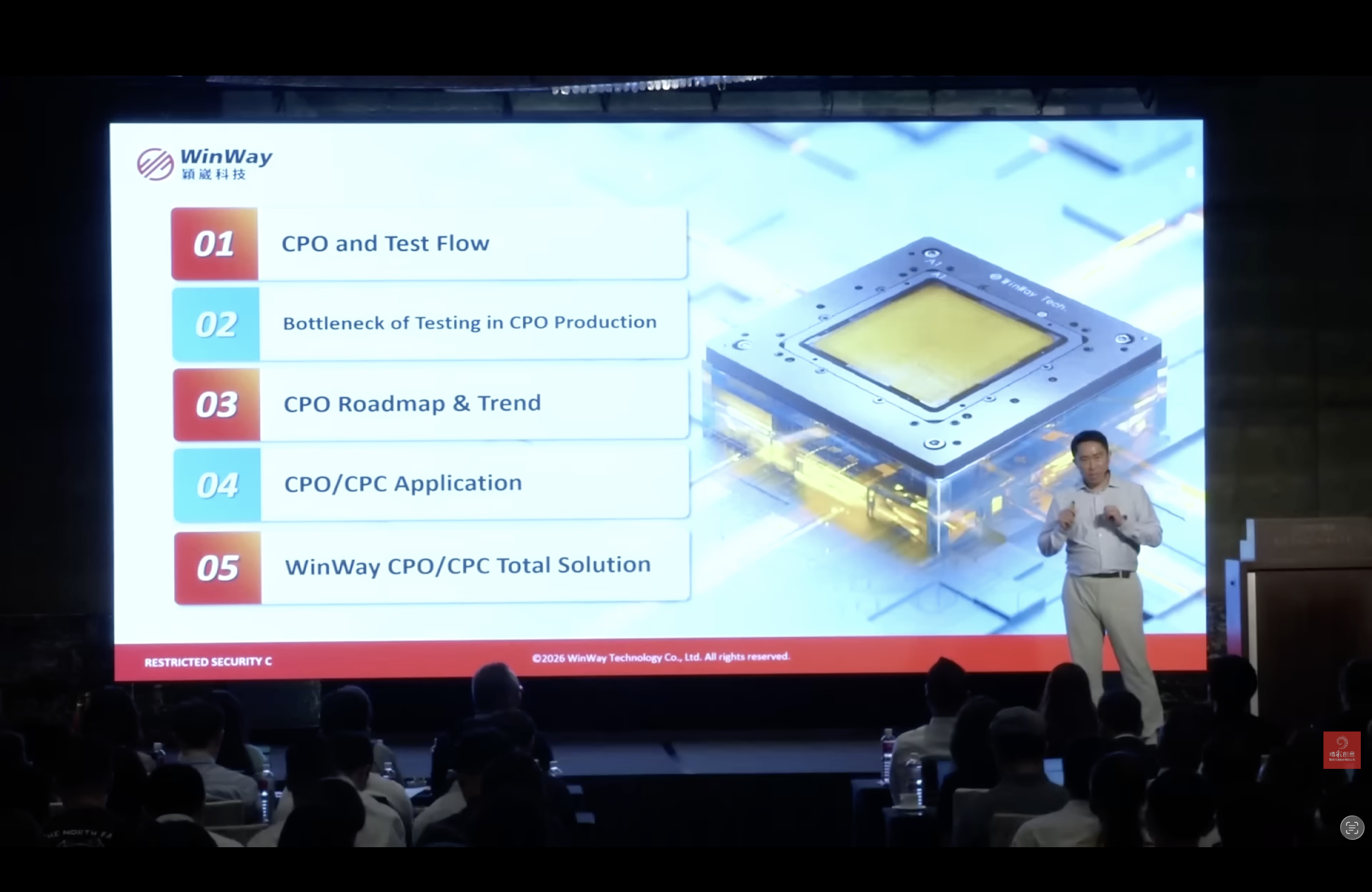
Winway is a testing equipment company based in Taiwan and it held a talk a while back to educate investors on CPO. You can watch the talk here. While the talk is delivered in Mandarin Chinese, the slides are all in English. That said, some of the nuances might be lost if you are not familiar with Mandarin Chinese with Taiwan specific lingo (例如,矽vs.硅), copackaged optics, or testing. So I will explain them with more context here after each slide if the slide itself is not obvious enough.
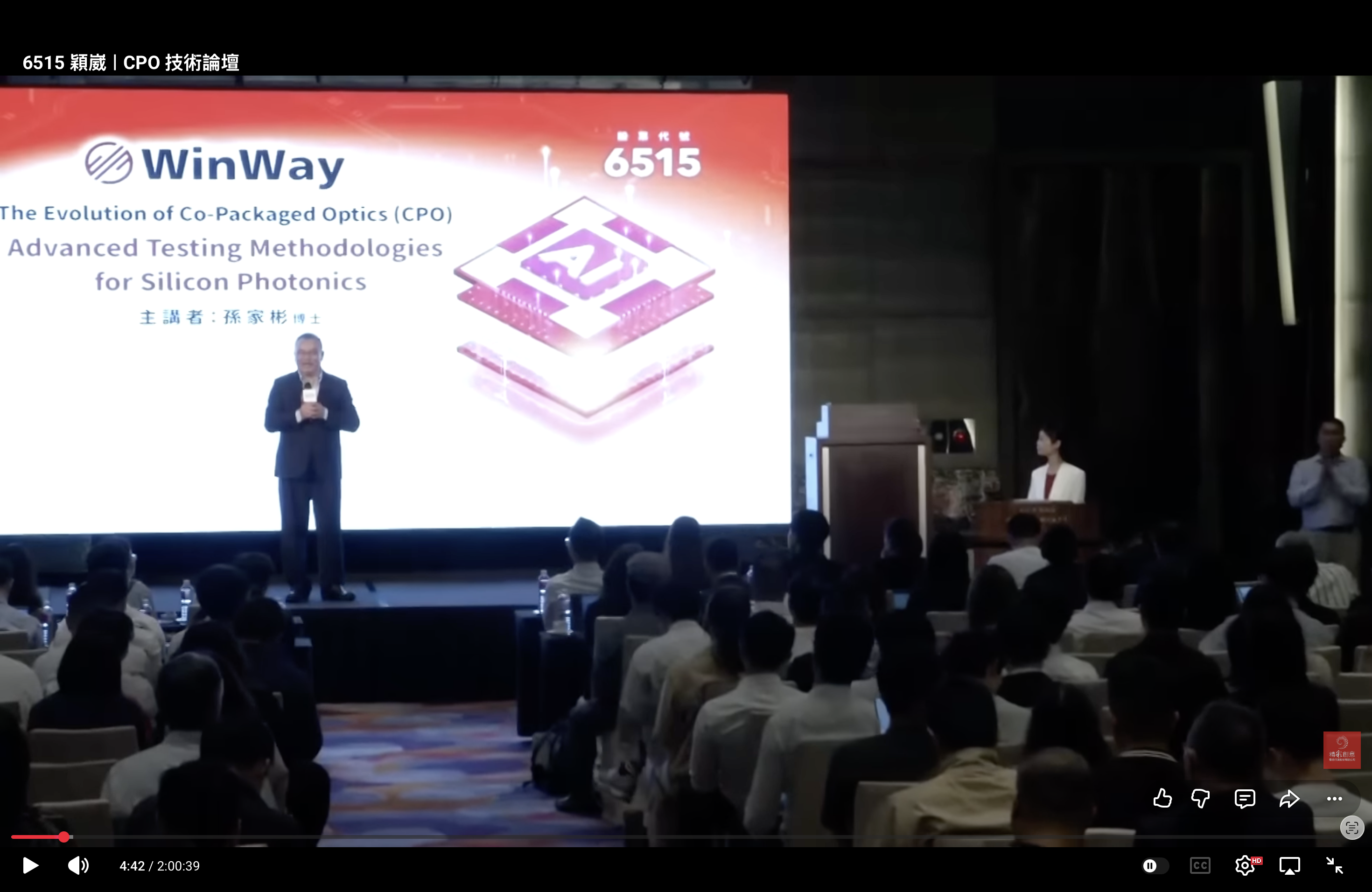
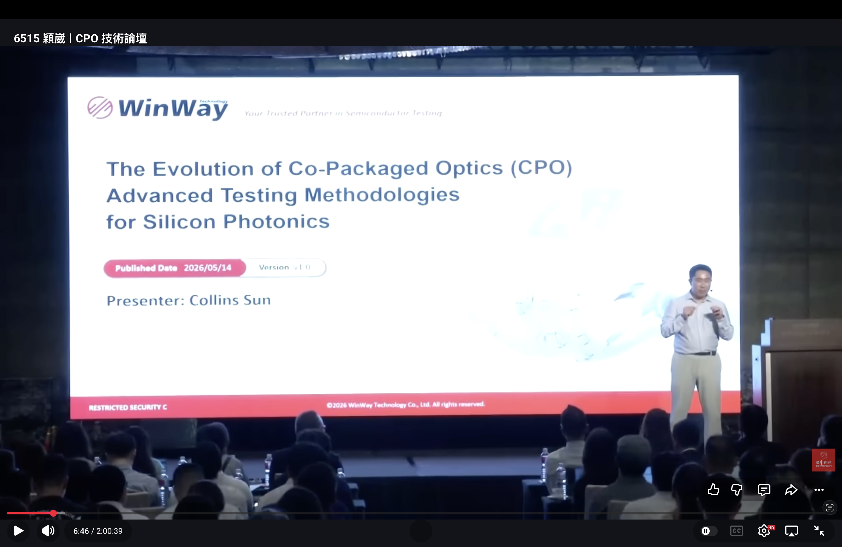
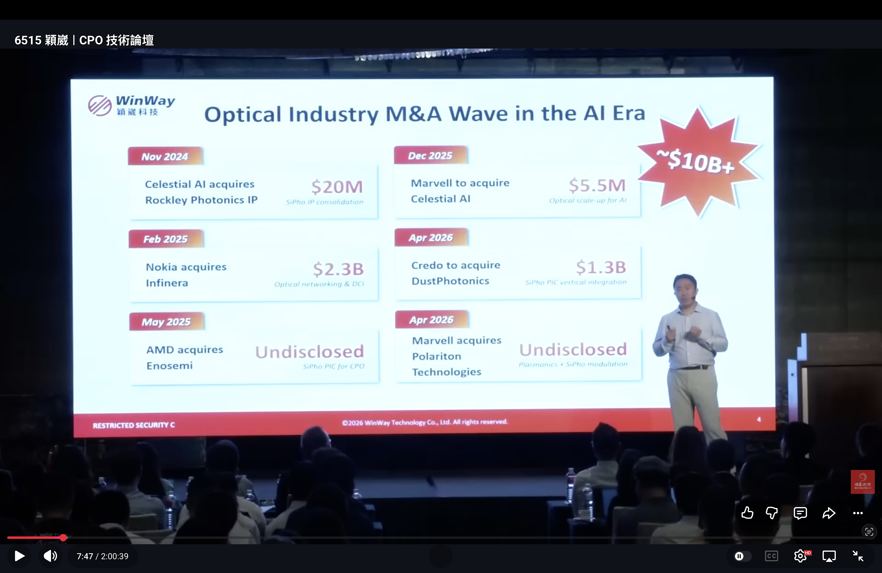
It is certainly an exciting time to be working or investing in the optics industry, given that the telecom boom and bust occurred a generation ago, during my childhood when I looked up to a certain Hong Konger called Charles Kao. Optics R and D takes a long time so it is almost always preferable to do mergers and acquisitions to acquire both the IP and experienced people to accelerate time to market.
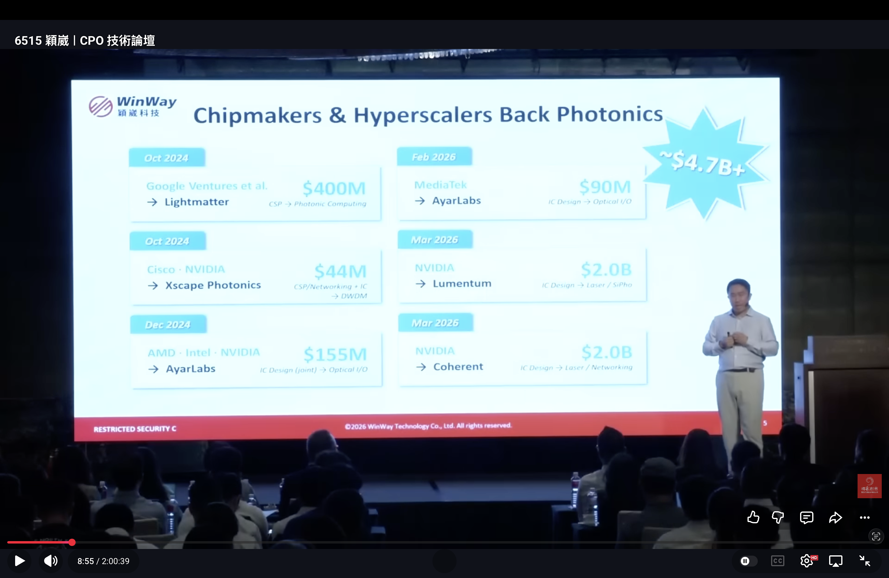
The big picture is that photonics is small but growing very fast relative to electronics, given the system level gains photonics unlocks.
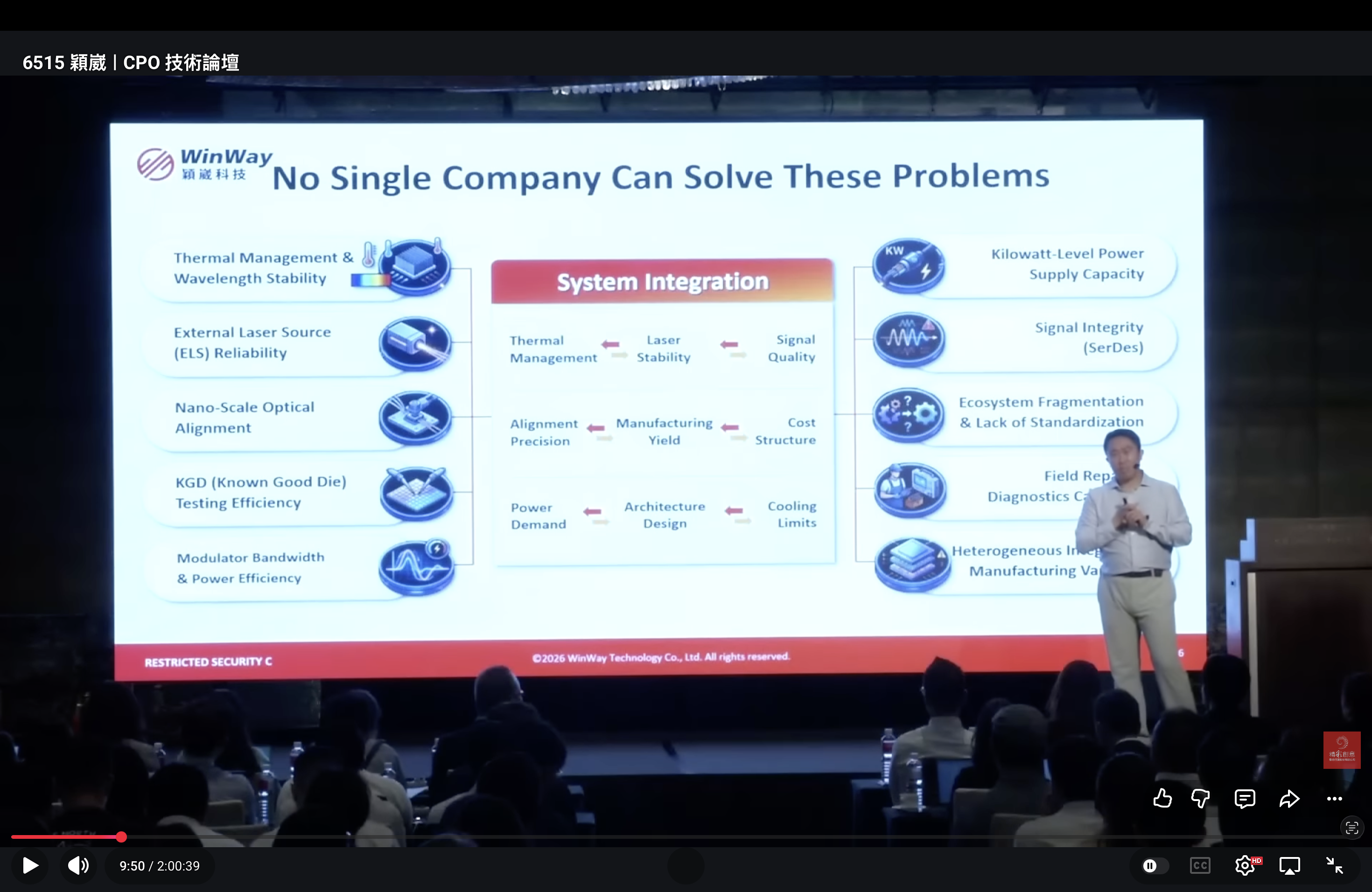
Yes, there are many engineering and economics challenges, some of which Collins Sun mentioned here. Challenges mean opportunities (危機-有危才有機) for those who can genuinely add unique value in this emerging supply chain.
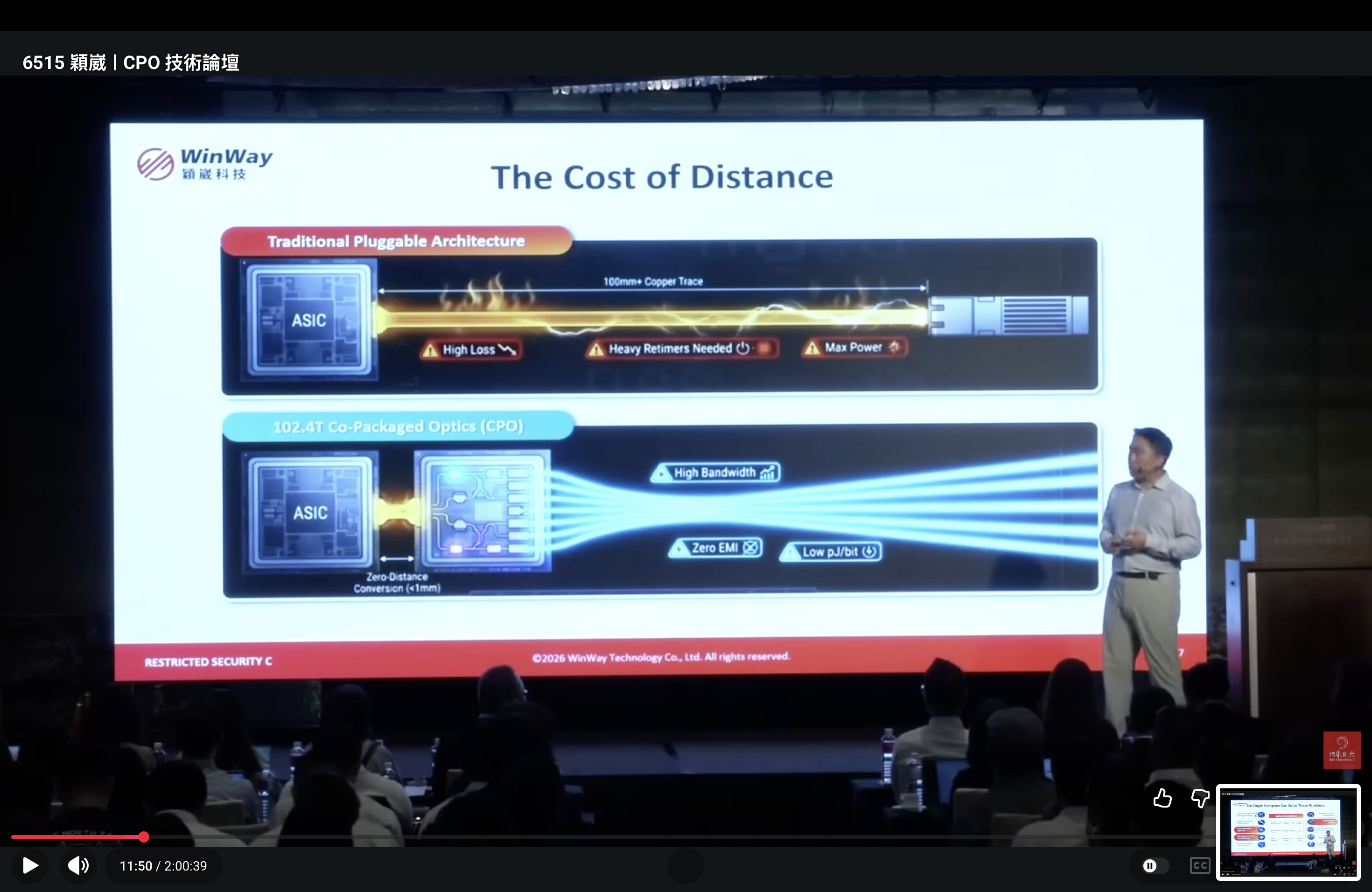
Those are the two relevant paradigms with the tradeoffs elucidated clearly. He skipped the half-steps (such as NPO, LPO, etc.) in the gradient from traditional pluggables to copackaged optics.
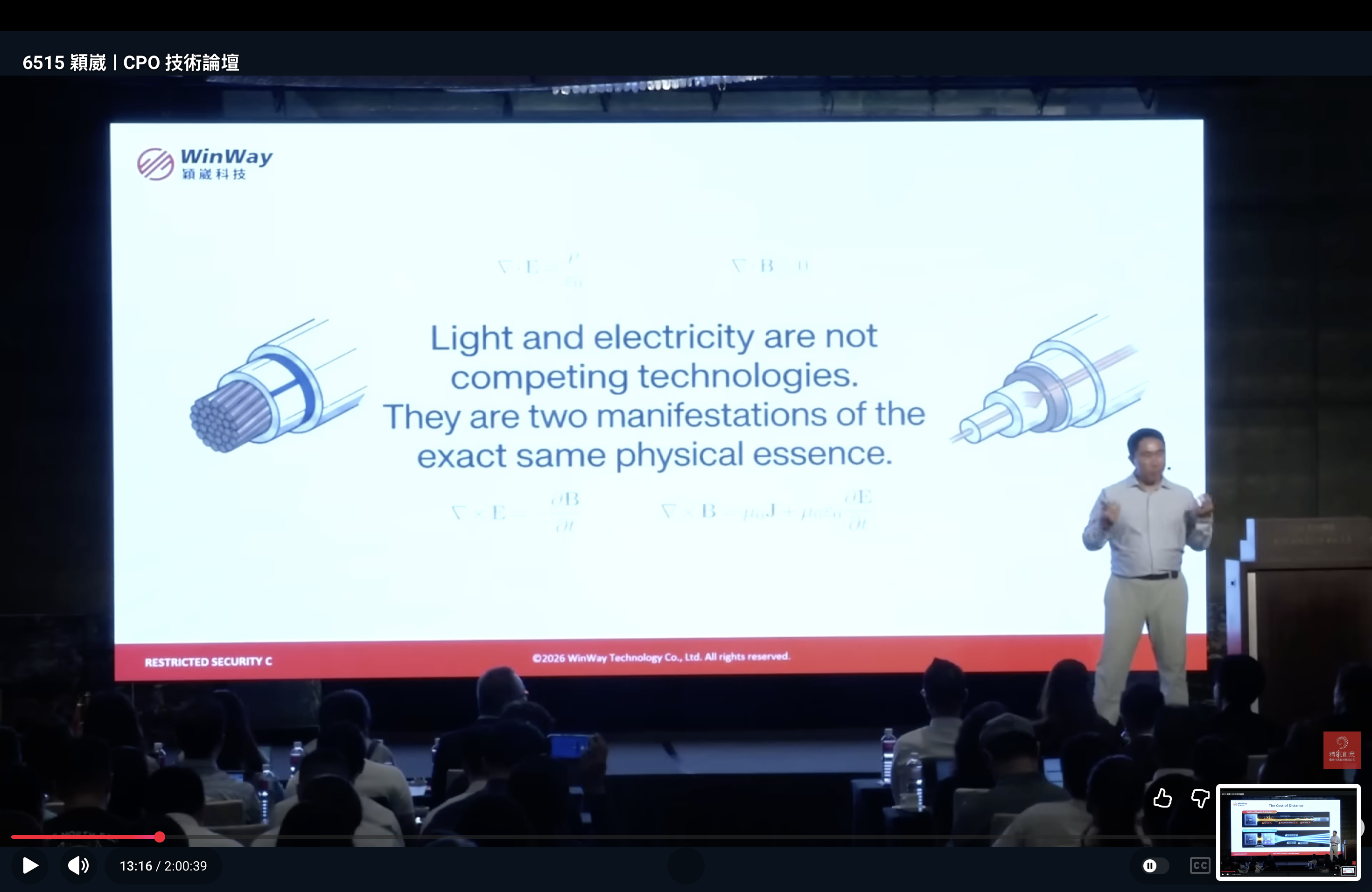
This should be obvious for anyone who studied electromagnetism at high school (Gymnasium/高中) or university level.
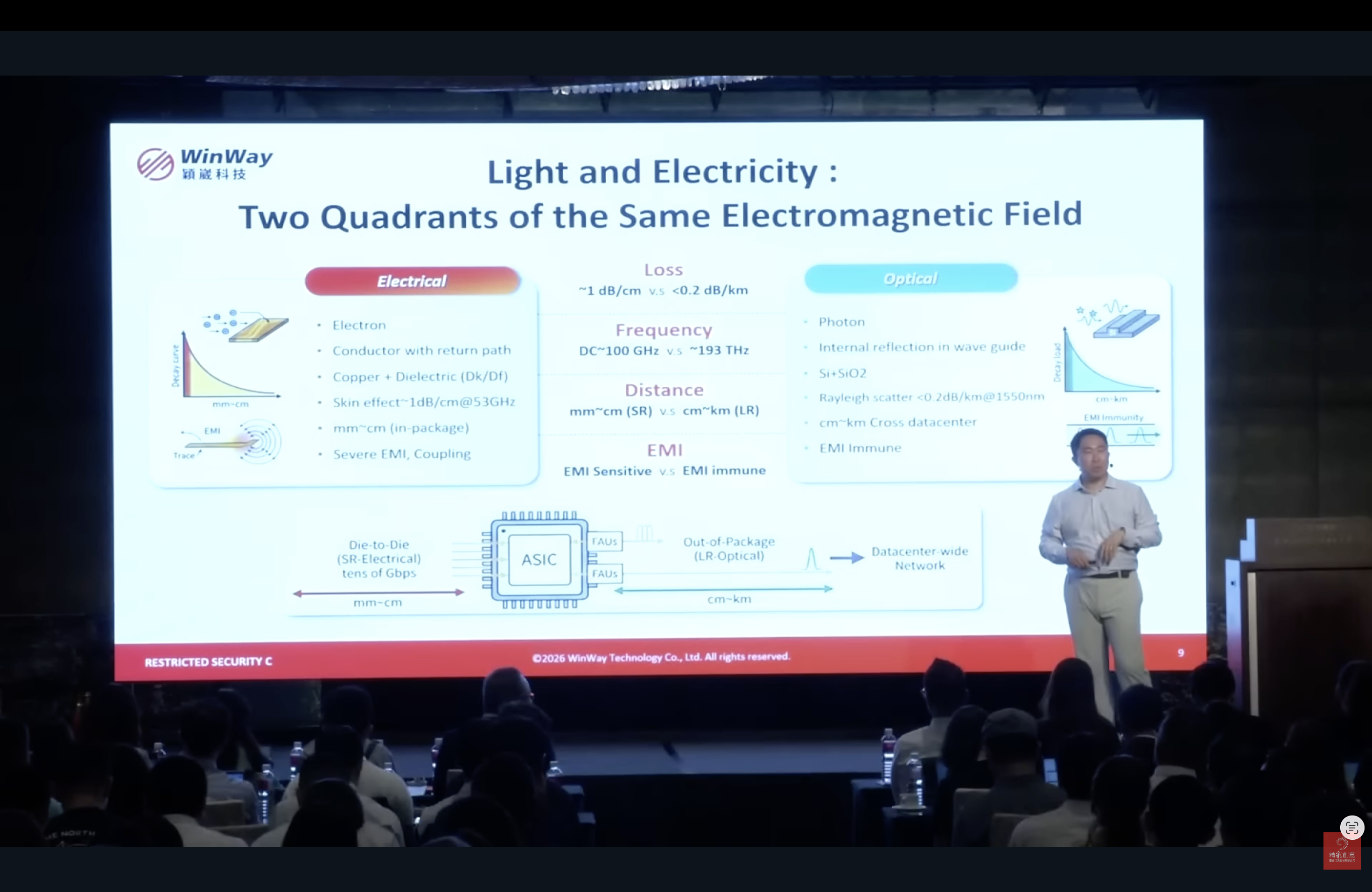
The general gist is that you can get way lower loss, higher frequency, longer reach, and EMI immunity with optics in principle.
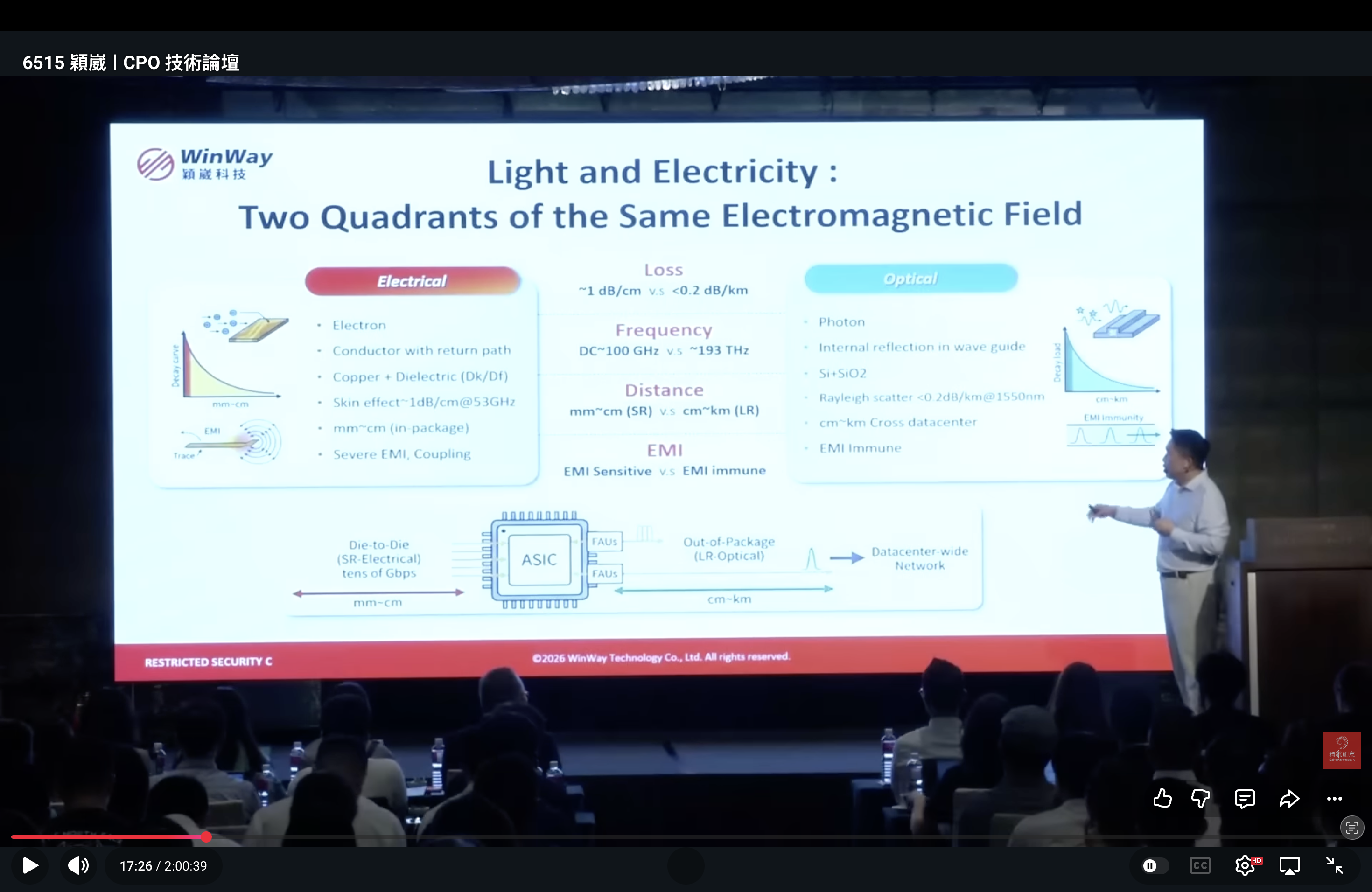
That aside, although they are both different manifestations of the same electromagnetic field, the actual engineering and economics differ significantly.
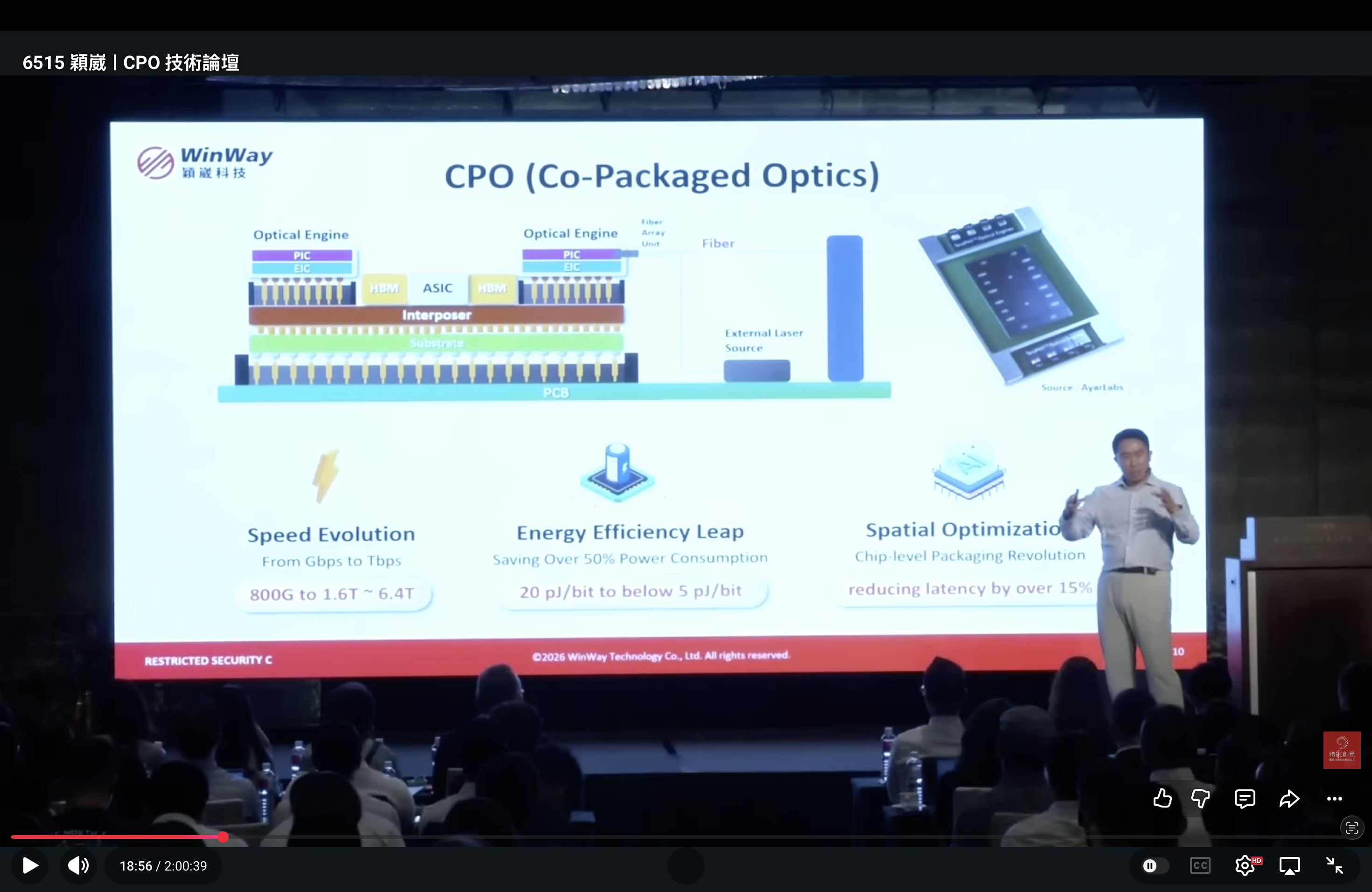
In principle, CPO brings system-level benefits for the next few generations of technologies relevant for the AI semis ecosystem. As I always reminded my aforementioned dear friend, what do you see in the idealized cross section of this CPO system?
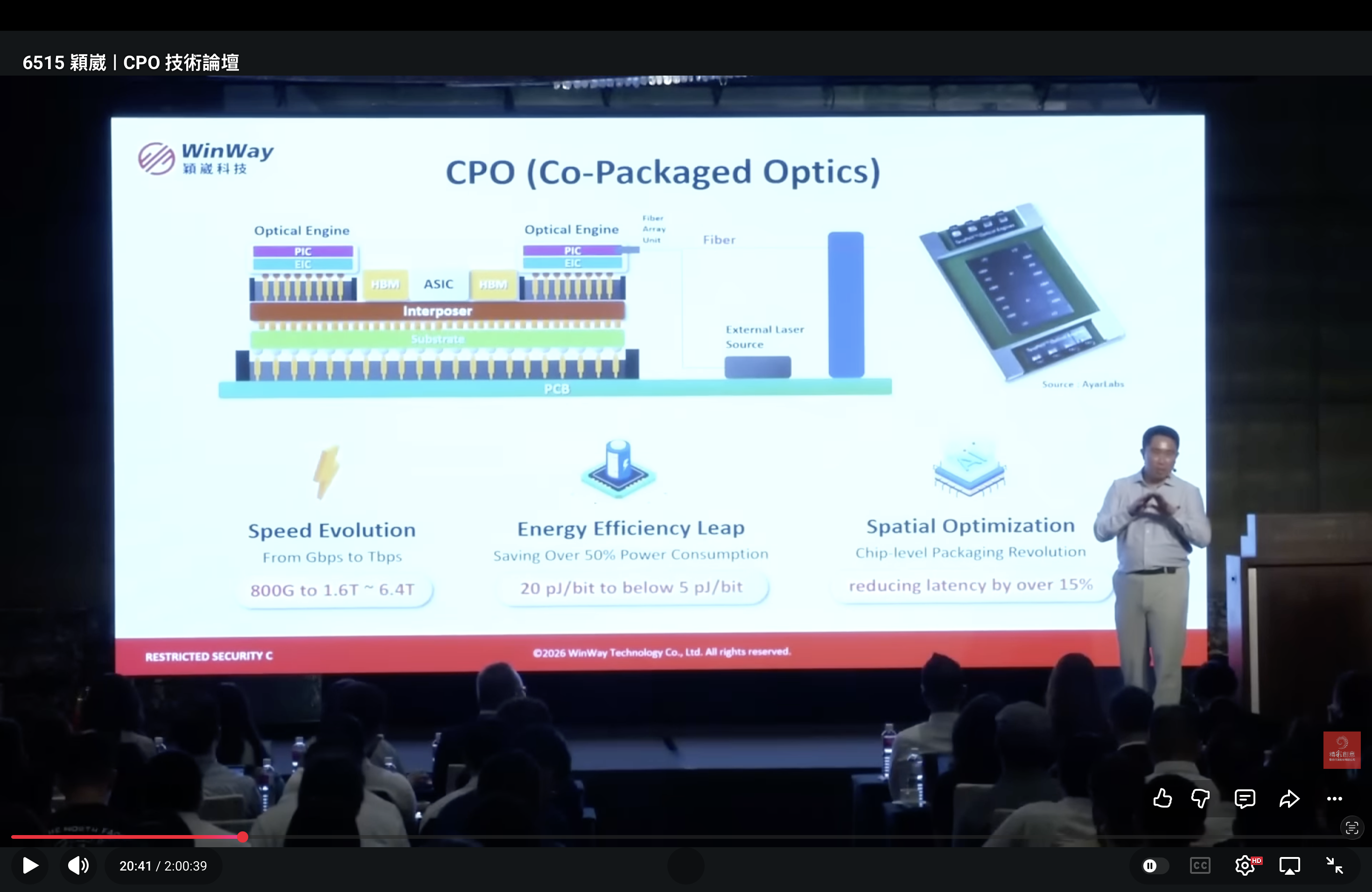
Notice where the laser source is? Why? This is an exercise left for the reader.
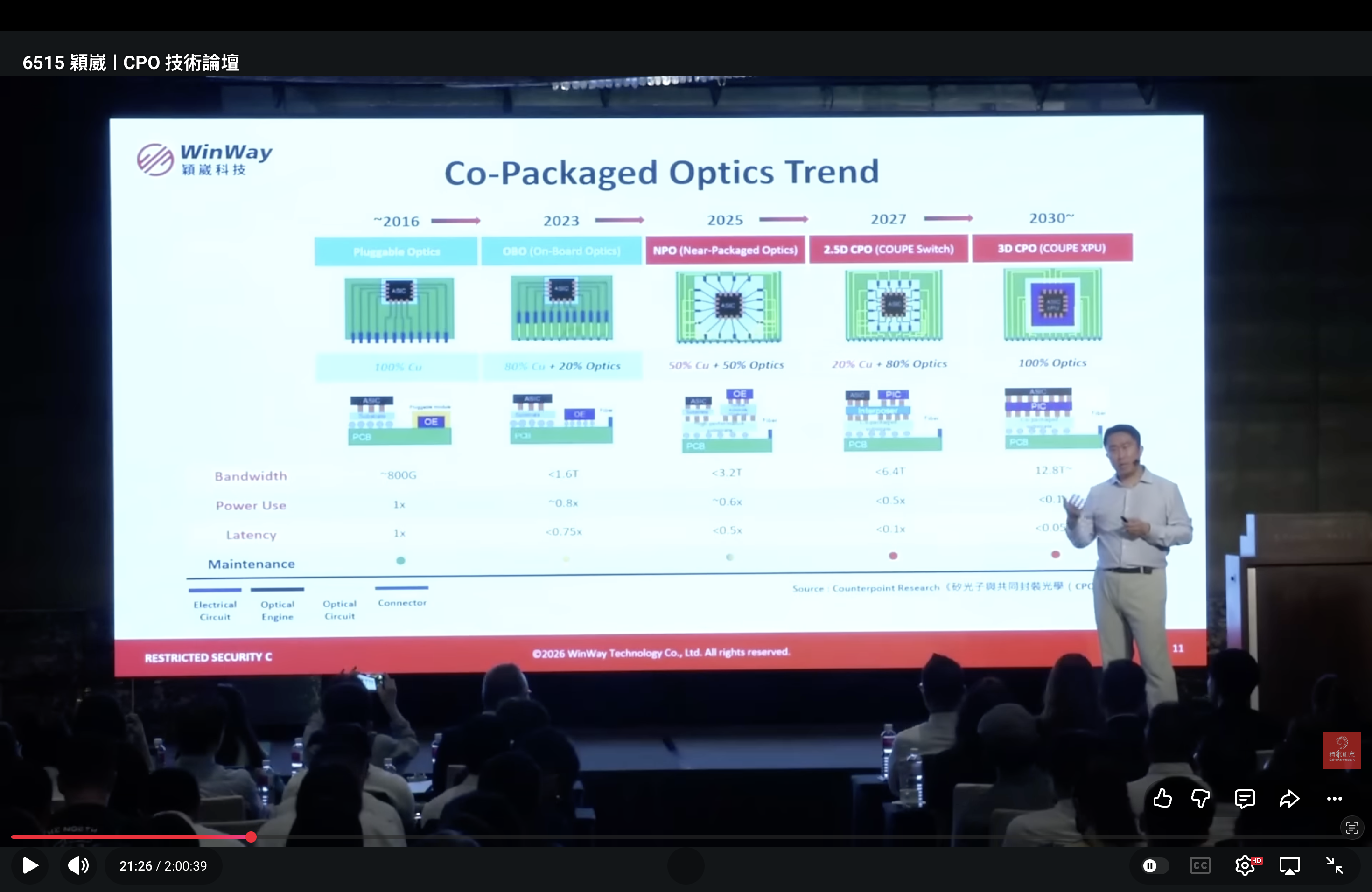
The general trend is for ever smaller form factor of the overall system which enable large improvements in bandwidth, power use, latency, and so on. Of course, the ones past today are just projections.
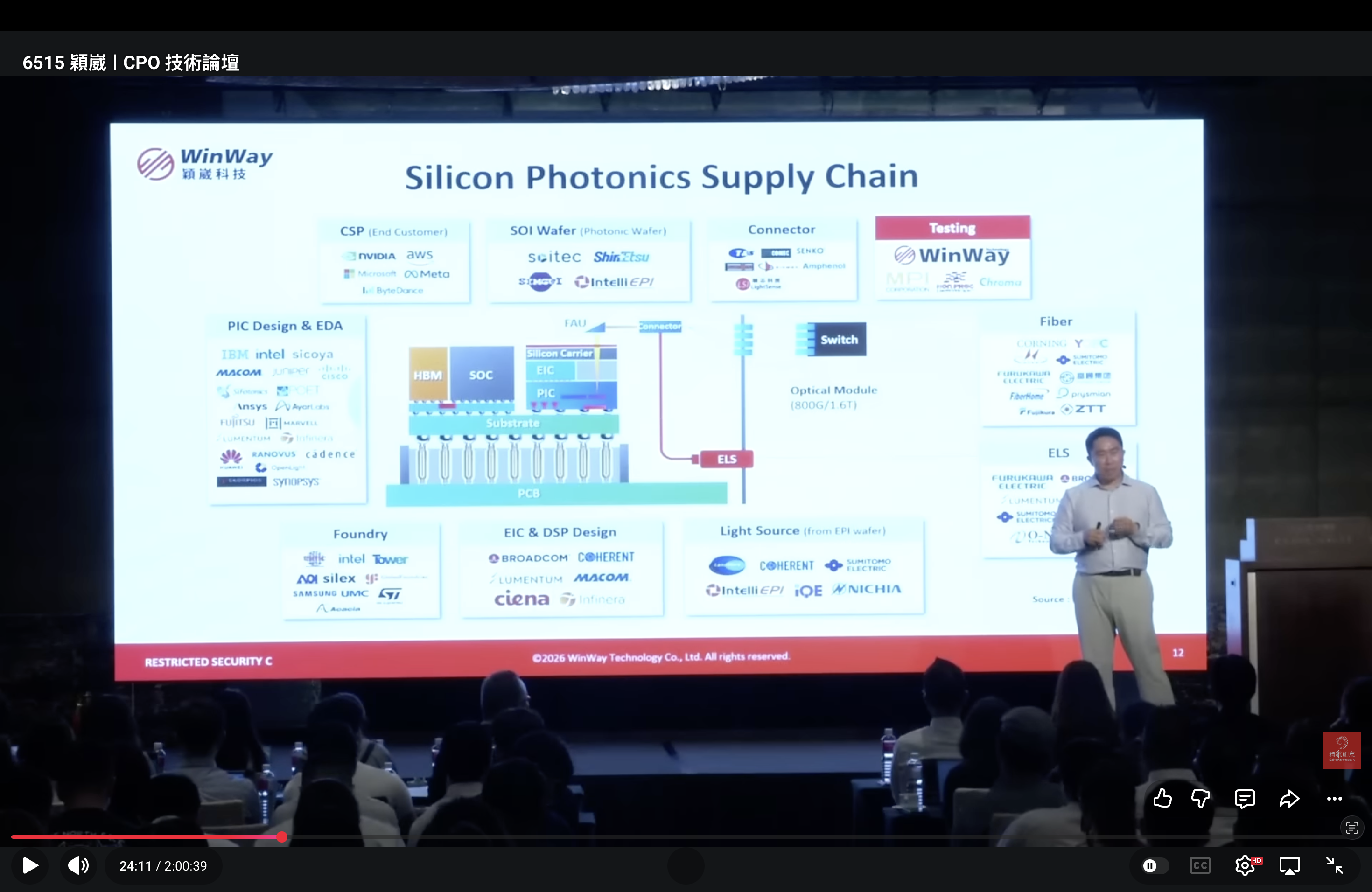
This is a very useful, but likely not comprehensive map of the silicon photonics supply chain. It looked a bit familiar from the ones from SEMIVISION and Leonardo Boquillón. In any case, I am working on my own map of the silicon photonics supply chain - stay tuned.
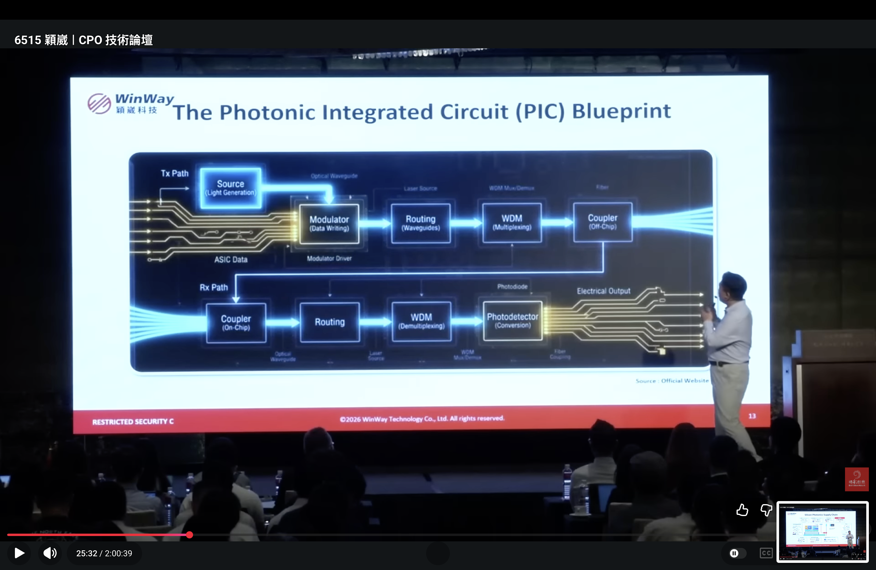
Here is a highly stylized schematic of what goes into a photonic integrated circuit - you can think of it as a chip for photons. DO NOT FORGET - there is always an electrical integrated circuit (EIC) that goes along with the photonic integrated circuit (PIC)! This sounds obvious, but lost on many ordinary folks. Of course, the overall insertion loss have to do with what materials platform you make the PIC out of and what fiber-to-chip couplers you use (most common are grating and edge couplers with pros and cons). For passive PICs, you want to use silicon nitride (specifically, deposited via low pressure chemical vapour deposition) waveguides for low loss, as Irrational Analysis may have mentioned before somewhere.
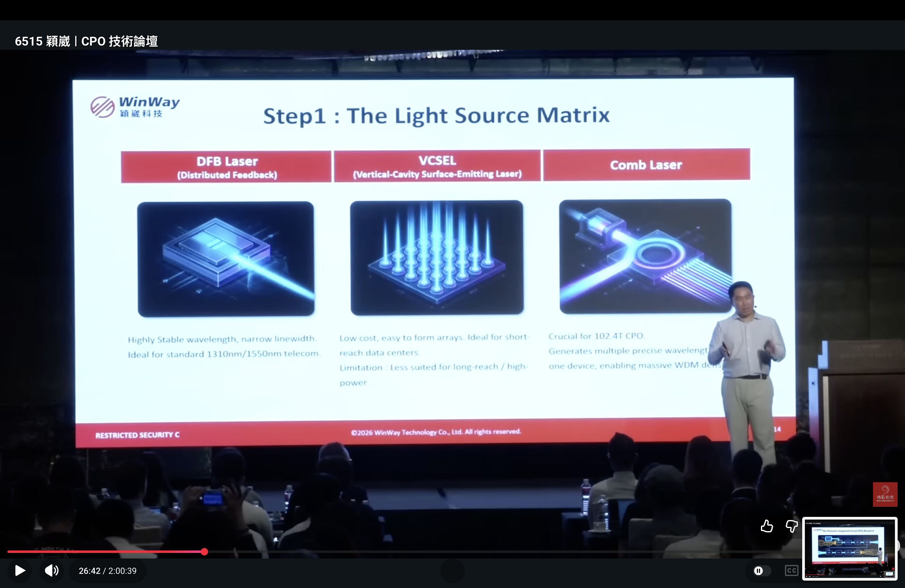
Yeah, that neatly summarises the tradeoffs among the different kinds of laser sources that are of course downstream of the underlying device physics and engineering choices which affect the overall economics. Again, just as before, I will like to remind my dear friend and other readers - just look at the cross section (especially of the relevant laser cavity).
Here is a summary of the different kinds of modulators. Real products made in high volume production amount to some point chosen on a tradeoff curve dictated by the underlying economics and engineering, which sit downstream of the device physics. Irrational Analysis wrote about this at some point, but you can look back at past Hot Chips Conference slides for similar information provided by the respective vendors. The more useful exercise, in my humble opinion, is to only look at revealed preferences - again, just look at the cross section of commercial PICs already produced in high volume and understand the fundamental reason why a modulator is used.
Yeah, this is fairly straightforward passive integrated photonics.
The idea here is that you can send more data at optical wavelengths by encoding them on light of different “colous” (wavelengths). In reality, each signal of a certain length has some finite spread, so the goal here is to minimise crosstalk between adjacent optical channels.
This slide tells you the gist of what you need to know. Grating couplers are the most scalable couplers if you can take the hit on insertion loss and bandwidth tolerance elsewhere in the system. They enable wafer level testing and packaging, which improve the overall manufacturability of the end CPO system. Of course, when overall insertion loss and polarisation insensitivity matter, edge couplers are preferred.
Yeah, there are different optical engines and optical engine connectors. Again, the engineering and economics differ significantly among the different integration schemes between EIC and PIC. The scalability of each EIC-PIC integration scheme is left as an exercise for the reader - again, what do you see in the cross section?
That is right - we are still in the early days with lots of spec diversity and customized solutions. Useful standards will only get determined by the vendor who ships first with the highest volume of quality products.
The reader should note that the silicon photonics related part of each PIC foundry/IDM is only a small (but vastly growing) part of each business. If any of you spent any time working or investing in a foundry or read Morris Chang’s memoir, you would know how important it is to be going up the learning curve as soon as possible. That said, I don’t know why the speaker left out Tower on this slide - go read Irrational Analysis who already wrote about it.
Yes, testing is a bottleneck in CPO production. I am just stating that this is a bottleneck solely on technical and economic considerations - nothing more and nothing less. Just stare at the cross section of a CPO system - how do you even know any of it works at all if you don’t test it at each step? Here is an excellent PIC Magazine piece from Andrew Yick (from Marvell) explaining how this works:
Here is a good summary slide on visualising the CPO test flow in addition to the one I have shown you earlier from Andrew Yick. Here is an exercise for the reader - what is the value of the inputs and the output of each step when constructing the CPO system? Again, just stare at the cross section…
From a practical system level perspective, you want to use single mode fiber (SMF), the most famous of which is Corning SMF-28 (but of course, there are other variants).
Yes, as someone used to rigor, I am delighted to see error bars because the engineers actually thought about manufacturability (design for manufacturability), testability (design for test), and scalability in the presence of variations that can be expected in high volume production settings. These quoted values are plausible values - for context, I have made V-grooves in silicon and used fiber arrays personally.
Again, reminder, there is little room in this field for amateurs who don’t appreciate the tolerances required to realize CPO systems.
Active alignment is largely a necessary evil, but it contributes to cost and throughput. Ideally, you don’t want to do that for a high volume commercial product if you can.
Here is the tradeoff between the two solutions.
Do not be fooled by how easy it looks as if it is like Legos - just no, these FAUs need to be very precisely aligned with the optical couplers on the PIC. Moreover, would they stay in place (post alignment) and not move that much after you apply (dispense and cure) some epoxy (basically glue)?
Yes, next time someone tells me about CPO, I will show them this slide. Again, my perspective is simple - more problems equal more opportunities for those who can add unique value for the end customers of CPO systems!
Just think about the opportunities here (imagine the testing intensity at each step) at each of the testing steps and levels - die, wafer, package, and module. Of course, this flow already exists for electronics, but the optics and optoelectronics testing market is still a blue ocean - go read the relevant posts written by my friends Fabian, Damnang, and PhotonCap.
Ideally, you want to do the test on the wafer level for high throughput in both the electrical and optical domains. As before, stare at the cross section!
Here is a slide on the die level test.
You still have to test more after you package the PIC and EIC.
Here is what package level test can look like.
Here is what module level test can look like. Again, I need to emphasize that it is not easy as it looks given the tolerances involved in CPO systems. I won’t comment on specific commercial products - do your own due diligence.
Here is a cross section of the COUPE platform from TSMC. As mentioned before, I like seeing grating couplers - why? Just stare at the cross section and this is left as an exercise for the reader.
Here is a projected CPO roadmap that shows what kinds of advances are needed to enable future technologies in the future.
That is right - it is tough to engineer the electro-optical interface. The future will require very close co-design by multidisciplinary folks with non-traditional backgrounds - say, T-shaped engineers like PhotonCap, Fabian, and Chad.
Don’t dismiss copper yet - optics and copper will coexist for a long time in different niches (reaches, etc.) and copackaged copper has a role to play. Again, stare at the cross section and see what pops out at you.
CPO and CPC have different vendors in their ecosystems.
Okay, he is now talking about what Winway has to offer.
I am always excited to see future technical challenges - that means more value will be accrued to companies who can actually execute and solve these valuable technical challenges for their customers. I won’t comment more other than saying solving these problems will require rare folks with firm understanding of the underlying fundamentals.
There are mechanical considerations to ever larger interposers (from TSMC) with demand driven by AI chips.
There are mechanical considerations to ever larger interposers (from Intel) with demand driven by AI chips.
Here are some of the tradeoffs among near term technologies in terms of electrical performance. Cleaner “eyes” are preferred in the context of optical communications.
Why can’t the industry just keep using copper? A few reasons listed here…
Pay attention to the SNR penalty and DSP complexity.
Just imagine the heat density for these next generation GPUs - what a exciting time to live if you are a thermal engineer!
Here are some of the considerations why some may consider glass as opposed to organic substrates (just go read any serious Taiwanese local media pieces on advanced packaging technologies from TSMC).
Amazing opportunity for those who can execute and deliver those advanced package test solutions for such packages (complexity grow as a function of size, pin count, speed, and heat density)!
These should look familiar to those already familiar with semiconductors testing - if not, go read my friend Damnang’s pieces.
He is talking about the product now, so I have no comment. The only thing that matters is whether their customers qualify their products for use on their products.
Perhaps I should go read the dry patents (some of which are probably in traditional Chinese) - had I understood the importance of traditional Chinese at the time in undergrad, I should have spent some time in Taiwan or my beloved HK (my alma mater UChicago has a center at Mt Davis 摩星嶺) then. On that note, I am currently reading this patent from Himax.
The talk was so long, but fine, it was a great two hour long talk.
This is a projected timeline - what an exciting time to live if you work or invest in photonics!
Again, just stay at the cross section!
Conclusions
In a sea of AI slop about such an important technology, I hope that this short piece can clarify a few things here and there. I can assert that none of this is written by AI and solely written by myself. Just as my younger self, I have always preferred to read only primary sources in the original language (English, Hochdeutsch, and 繁中) and make my own independent judgments about technologies actually from first principles in terms of the underlying physics, engineering, and economics. As a reminder, I will be in the Bay Area this weekend - specifically, South Bay (Palo Alto, San Jose, Santa Clara, etc.) on this Saturday 6/6 and San Francisco on this Sunday 6/7 (feel free to DM me for coffee or something if like minded readers are in the area).
第二部分:解析(深度解读)
一、这篇文章为什么重要
本文作者 Jack Huang 是少数同时具备物理/数学学术训练、EDA(电子—光子设计自动化)产业经验、以及德语区(DACH)精密光学文化语感的英文写作者。他用「能力圈(circle of competence)」原则写作:只对既懂理论又懂工程实践的主题发言,并且明确表示不会免费逐一反驳读者(卖方、买方、CPO 公司内部人士)的观点。这种立场在当下充斥「AI 噱头」的 CPO 讨论中相当稀缺。
文章的核心素材是台湾测试设备厂 WinWay(穎崴)面向投资者的一场 CPO 科普宣讲(含两小时 YouTube 视频)。作者逐页解读幻灯片,反复用一句话点题——「盯着横截面看(stare at the cross section)」。这句话的实质含义是:CPO 不是抽象概念,而是材料、器件、耦合、封装、测试在纳米—毫米尺度上高度集成的系统工程,只有回到物理横截面,才能看清单点失效与良率瓶颈究竟在哪里。
文章最有价值的一句警示,是用大立光(Largan)作为反面教材:一家精密光学高管「事后才发现」CPO 是高精度、高资本开支、强专有知识(knowhow)的生意。这恰好说明——在 CPO 投资里,「搞懂基本面」本身就是一种竞争优势,而非可有可无的前置条件。
二、核心论点拆解
| 论点 | 作者的判断 | 投资含义 |
|---|---|---|
| CPO 的系统级收益 | 更小外形、更高带宽、更低功耗/延迟,面向 AI 半导体生态未来几代技术 | 长期确定性高,但兑现节奏取决于工程与成本曲线 |
| 演进范式 | 从可插拔(pluggable)→ CPO 的梯度;作者指出演讲者跳过了 NPO/LPO 等中间形态 | 中间形态(LPO/NPO)仍可能切走一部分近中期需求 |
| PIC 永远配 EIC | 光子集成电路必有对应的电集成电路,插入损耗取决于材料平台与光纤—芯片耦合器 | 单一维度领先不够,需看 EIC-PIC 协同 |
| 激光源 / 调制器 | 选择是底层器件物理与工程经济学的下游结果;应看「已量产商用 PIC 的横截面」倒推真实偏好 | 看多「revealed preference」而非 PPT 参数 |
| 耦合器:光栅 vs 边缘 | 光栅耦合器最可规模化(支持晶圆级测试/封装),代价是插入损耗与带宽容差;边缘耦合器在损耗与偏振不敏感上占优 | 光栅耦合器路线利好晶圆级测试设备 |
| 测试是瓶颈 | 从 die / wafer / package / module 每一级都要测,否则无法证明系统可用 | 直接指向 WinWay 这类测试设备厂的总可寻址市场 |
| 标准未定 | 早期 spec 高度分散,谁先以最高质量批量出货,谁定义标准 | 先发批量出货者掌握话语权 |
| 铜与光共存 | 不要急于宣判铜「死刑」,共封装铜在部分 reach 仍有角色 | 抑制「光全面替代铜」的过度乐观 |
三、关键概念 / 技术解读
CPO(Co-Packaged Optics,共封装光学):把光引擎与交换芯片/ASIC 封装在一起,替代可插拔光模块,以缩短电走线、降功耗、提带宽。作者强调其「系统级收益」建立在极低损耗与 EMI 免疫之上。
PIC 与 EIC:PIC(Photonic Integrated Circuit)是「光子的芯片」,但永远配套一颗 EIC(Electrical IC)做驱动与信号处理。整体插入损耗由「PIC 材料平台 + 光纤—芯片耦合器」共同决定;无源 PIC 倾向用 LPCVD(低压化学气相沉积)氮化硅波导以获得低损耗。
耦合器(Coupler):最常见是光栅耦合器(grating coupler)与边缘耦合器(edge coupler)。光栅耦合器胜在可晶圆级测试与封装(提升制造良率与可扩展性),代价是插入损耗与带宽容差;边缘耦合器在插入损耗和偏振不敏感上更优。作者特别点出 TSMC 的 COUPE 平台横截面里能看到光栅耦合器——这并非偶然,而是为晶圆级可测试性服务的工程取舍。
FAU 与主动对准:FAU(Fiber Array Unit,光纤阵列单元)必须和 PIC 上的光耦合器极高精度对齐,贴装后还要靠环氧树脂(胶水)固化「锁死」位置、防止漂移。主动对准(active alignment)是「必要之恶」,拉高成本、拉低吞吐——理想的高批量产品应尽可能规避。
波分复用(WDM)与串扰:用不同波长(”colous”)在同一光纤上承载更多数据,但每个信道有有限谱宽,目标是最小化相邻光信道间的串扰(crosstalk)。
SMF-28:单模光纤的事实标准(Corning 出品),实际系统层面倾向使用单模光纤。
测试金字塔:die → wafer → package → module 四级都要测。电子测试流程已成熟,但光与光电子测试仍是蓝海——这正是作者反复强调的机会所在。
玻璃基板 vs 有机基板:随 AI 芯片推动更大 interposer(TSMC、Intel 路线),机械应力/翘曲成为问题,部分场景考虑玻璃基板。复杂度随尺寸、引脚数、速率、热密度上升,直接放大先进封装测试需求。
四、与本站其他 CPO / 硅光系列文章的链接
- CPO 最大瓶颈:高量产测试(cpo-biggest-bottleneck-high-volume-testing) — 与本文「测试是 CPO 量产瓶颈」的核心论点直接呼应,可互为印证。
- CPO 幻象?CPO 专题终章(the-illusion-of-cpo-cpo-special-final) — 补足对 CPO 落地节奏与「幻象」的批判性视角。
- 光学入门(三):共封装(optics-primer-part-3-co-packaged) — 回顾可插拔→CPO 的范式演进与 tradeoff。
- 台积电领跑 CPO、三星第三芯片(tsmc-ahead-in-cpo-samsung-third-chip) — 对应文中 TSMC COUPE 平台与 interposer 机械议题。
五、投资意义
- WinWay(穎崴,测试设备):本文最直接的标的。文章标题即「WinWay CPO Talk」,核心结论是测试是 CPO 量产的硬瓶颈,而 CPO 系统尺寸/引脚/速率/热密度越高,先进封装测试需求越大。WinWay 的 TAM 与 CPO 放量节奏强相关;但作者也点明,最终只看「客户是否把其产品认证(qualify)用于自家产品」——需跟踪客户认证进展。
- ASMPT(港股 00522):作者点名香港新界青衣的 ASMPT,称其「规模小但在 CPO 上的敞口正在增长」,属封装/贴装设备侧的观察对象。
- Tower Semiconductor:作者批评演讲者漏掉了 Tower——呼应 Irrational Analysis 的覆盖,意为代工环节的硅光产能不只看台积、Intel,Tower 也是变量。
- TSMC(TSM)/ Intel(INTC):COUPE 平台横截面、以及随 AI 芯片放大的大尺寸 interposer 机械议题,直接利好两家先进封装路线。
- Corning(GLW):SMF-28 单模光纤是系统层面的默认选择,光互联放量对其光纤业务为正向。
- Marvell(MRVL):文中引用其 Andrew Yick 关于可扩展光测试的 PIC Magazine 文章,凸显其在 CPO 测试方法论上的话语权。
- Himax(HIMX):作者正在研读 Himax 的台湾专利,提示其在光/显示相关 IP 上的潜在价值。
- 反面教材 Largan(大立光,3008.TW):说明精密光学龙头跨界 CPO 也会因「高精度 + 高资本 + 强 knowhow」而踩坑,投资时勿以传统光学经验线性外推。
六、风险提示
- 标准未定 / spec 分散:行业早期,无统一标准,先发高批量出货者定义规则,后发者面临路线被否风险。
- 高精度、高资本、强 knowhow:CPO 不是「像乐高一样拼装」,FAU 对齐、环氧固化、主动对准都容错极低,执行风险显著高于普通封装。
- 铜光共存:共封装铜在部分 reach 仍有角色,「光全面替代铜」是过度叙事,可能压缩近中期光模块/光引擎的替代斜率。
- 测试设备需求依赖放量:WinWay 等测试厂的天花板取决于 CPO 实际量产节奏;若 CPO 商用推迟,设备订单将后移。
- 认证不确定性:作者明确——设备厂产品是否被客户认证用于其产品,才是唯一要紧的事,需以客户认证与营收兑现为证。
- 信息完整性:本文英文为免费全文(无付费墙);原站前半部分配图(至 PIC/EIC 示意图及其后一张激光源权衡幻灯片为止,共 18 张)已按原站幻灯片位置嵌入,其后幻灯片因抓取环境限制暂未取回,读者应回原站视频/幻灯片交叉验证。
以上解读基于原文信息整理,不构成投资建议。