A Complete Technical Overview of Advanced Packaging and Heterogeneous Integration — 先进封装与异构集成完全技术概览
整理自 Silicon Co-Design(Chad):从 2D 到 3.5D 的先进封装与异构集成分类、TSMC 2.5D CoWoS 拆解(TSV 制造、RDL 工艺、C4/C2 凸点),以及基板瓶颈。英文原文(免费部分)+ 中文深度解读;🔒 付费段(玻璃基板、面板 vs 晶圆、有机基板内嵌桥、混合键合工艺)未包含。
本文整理自 Silicon Co-Design(作者 Chad,Substack 技术专栏),原文发布于 2026-06-09。 标题原文:A Complete Technical Overview of Advanced Packaging and Heterogeneous Integration(URL slug 为
a-masterclass-on-advanced-packaging)。 结构为 正文(英文原文)+ 解析(中文深度解读),方便中英对照阅读。 ⚠️ 本文为付费专栏,公开免费部分止于「Substrate Options」章末;🔒 付费段(Glass Substrate、Panel or Wafer、Embedded bridge in Organic Substrate / CoWoS-L vs EMIB-T、Hybrid Bonding 工艺步骤)位于付费墙之后,本发布未包含任何付费内容。文中 7 张配图(Figure 1–7)均在免费段内,已解码为 S3 直链嵌入。
第一部分:正文(Original Article)
A Complete Technical Overview of Advanced Packaging and Heterogeneous Integration
From 2D to 3.5D, a teardown of 2.5D CoWoS (TSV, RDL, Bump/pillar) and emerging trends (Glass, Panels, Bridges in Organic Substrate, and Hybrid Bonding)
In this post I’ll build intuition of the key tradeoffs and constraints surrounding advanced packaging.
- I’ll define each of the classifications at a high level (from 2D to 3.5D)
- Then I’ll do a breakdown of each of the key options of a TSMC 2.5D CHIP on WAFER on SUBSTRATE (CoWoS). We will examine this package architecture through the following lens:
- TSV Fabrication
- RDL Fabrication (with BEOL Process for Si)
- Interconnect Options (C4 Bump, C2 Cu Pillar)
- 🔒Substrate Options
- 🔒Glass Substrate and the unique challenges: SeWaRe and bump reliability
- 🔒Panel or Wafer - Why we didn’t do panels in the first place
- 🔒Embedded bridge in Organic Substrate
- 🔒TSMC CoWoS-L vs Intel EMIB-T
- 🔒The Process Steps for Hybrid bonding and why it isn’t widely adopted
The reason I write this post is to establish some fundamentals of advanced packaging and communicate what a packaging engineer would like other engineers to know who are interfacing with packaging. My goal is to build on top of the knowledge on this post as well as my existing posts to be able to understand how to properly co-design electronics with the package.
Please note that I do not consider myself an expert in advanced packaging by any means. I reference John Lau’s slides from his seminar at ECTC 2026 and my overall conference experience to better understand the interactions with advanced packaging and other domains.
If you’re an expert and notice something incorrect, please reach out to me so I can have it promptly corrected.
Advanced Packaging is like City Planning
Advanced Packaging is a lot like city planning:
- In rural areas, houses and buildings are distributed across a large plot of land (2D)
- In suburbs, houses and mid-sized buildings are bundled closer together and connected (2.1, 2.3, 2.5D)
- In cities, floors are stacked both above and below with means to access them (3D, 3.3D, 3.5D)
City planning is all about managing the flow of people to and from desired destinations.
Advanced packaging follows the same logic: signals need to get to and from compute devices. However, there is an order of magnitude difference between the dimensions of the on-chip interconnect and the PCB/package interconnect. As speed and power requirements increase, more sophisticated and elegant means of package interconnect are needed to bridge this order of magnitude difference.
Just like any building, as you start stacking floors, the structural stability needs to be considered with appropriate safety factors designed in. This logic also applies to advanced packaging as factors like reliability, thermal, and mechanical characteristics become more important.
High Level Classifications: From 2D to 3D
There are several structural variants of advanced packaging. All of these build the system on top of a build-up package substrate on top of a PCB.
Why do you need a buildup package substrate? There are a few reasons:
- Package substrates help “bridge” the dimensional order-of-magnitude gap with the chip level interconnects and the board level traces. This is done through “fan out connections” where the package solder balls spread the signals out from underneath a chip.
- Mechanical Buffer. The package acts as a buffer to protect the chip against stress, vibration and thermal effects. The coefficient of thermal expansion is an important consideration. We’ll see how, quite paradoxically, the low CTE of glass can have a negative impact on reliability.
- Local interconnect amongst chiplets. This is done through a combination of Re-distribution layers (RDLs) and Back-end-of-line (BEOL) metallization on Si Wafers
2D Integration
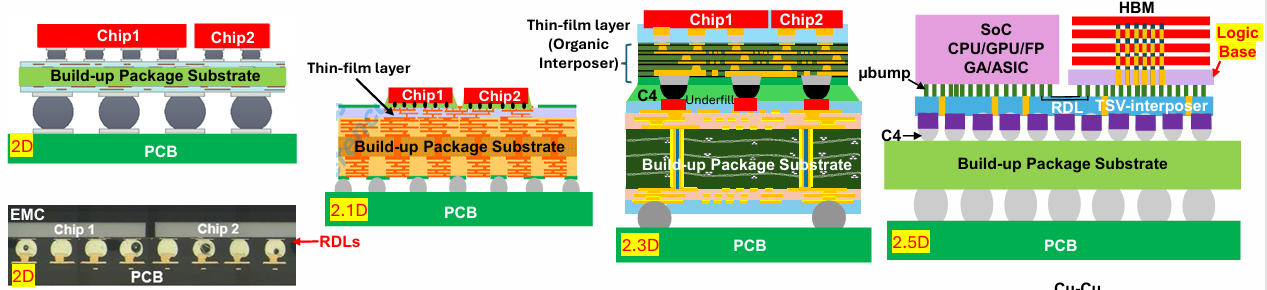
Figure 1. 2D classifications. Source: Lau. J. (Unimicron) “Advanced Packaging for Chiplets, Heterogeneous Integration, and Co-packaging Optics” ECTC 2026
2D packaging represents the historical and architectural “baseline” packaging technology that more advanced variants build off of. In 2D we have the following classifications:
- 2D - the chip is bonded directly on top of a build-up package substrate.
- 2.1D - the RDLs (Redistribution Layers) are built as thin film layers directly on top of the organic substrate itself.
- 2.3D - The RDLs are fabricated separately on an organic interposer on top of a build-up package substrate. This is also known as the “hybrid approach”.
- 2.5D - The chips themselves sit directly on top of a massive, monolithic Silicon Core (Silicon Interposer) or a Glass Core (Glass Interposer)
In 2.1D and 2.3D, two popular materials used in the dielectric films are ABF and PID.
- Ajinomoto Build-Up Film (ABF) is a resin-based epoxy film embedded with silica fillers.
- ABF has exceptional mechanical stability, excellent thermal resistance, and a low Coefficient of Thermal Expansion (CTE)
- Photoimageable Dielectric (PID) is almost chemically similar to photoresist; it is a liquid polymer or dry film that is chemically engineered to react directly to light.
- PID can be made much finer than ABF, but is traditionally mechanically weaker than ABF.
There is a core mechanical stability vs feature size tradeoff between both films. ABF tends to be the dominant choice of packaging due to its ability to handle many metal layers.
2.1D / 2.3D are considered to be low cost alternatives to 2.5D, which is considered the standard for AI/HPC.
3D Integration
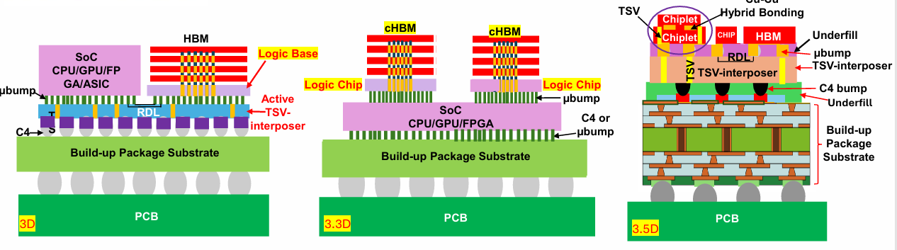
Figure 2. 3D Classifications. Source: Lau. J. (Unimicron) “Advanced Packaging for Chiplets, Heterogeneous Integration, and Co-packaging Optics” ECTC 2026
3D enables more computational density to be stacked in the vertical direction. The higher order classifications in 3D are still emerging and contested, but this is what Lau preliminarily defines:
- 3D - stacking chiplets directly on top of each other vertically on an active interposer (compared to 2.5D which is passive). These active interposers can contain IVRs, NoCs, BIST, or other peripheral circuitry that complement the functions of the SoC.
- 3.3D - consists of HBM on top of an SoC without a TSV interposer
- 3.5D - Involve hybrid bonding chiplets before integrating heterogeneously all components onto a single substrate.
As packages becoming increasingly integrated with the chip themselves, this leads to one of the biggest packaging challenges: whose responsbility should be for final assembly of the packaging: the fab, or the OSAT? Historically, both fab and OSAT specialized in different parts of the semiconductor production flow. The fab specialized in short pitch, finer interconnects and the OSAT specialized in higher pitch, coarser interconnects.
When hybrid technologies such as bridges and LSI in organic substrates come along, who will assume responsibility for final package integration? This is a question that is still being fiercely debated among the fab and packaging community and will be left for another time.
A Package Teardown: 2.5D
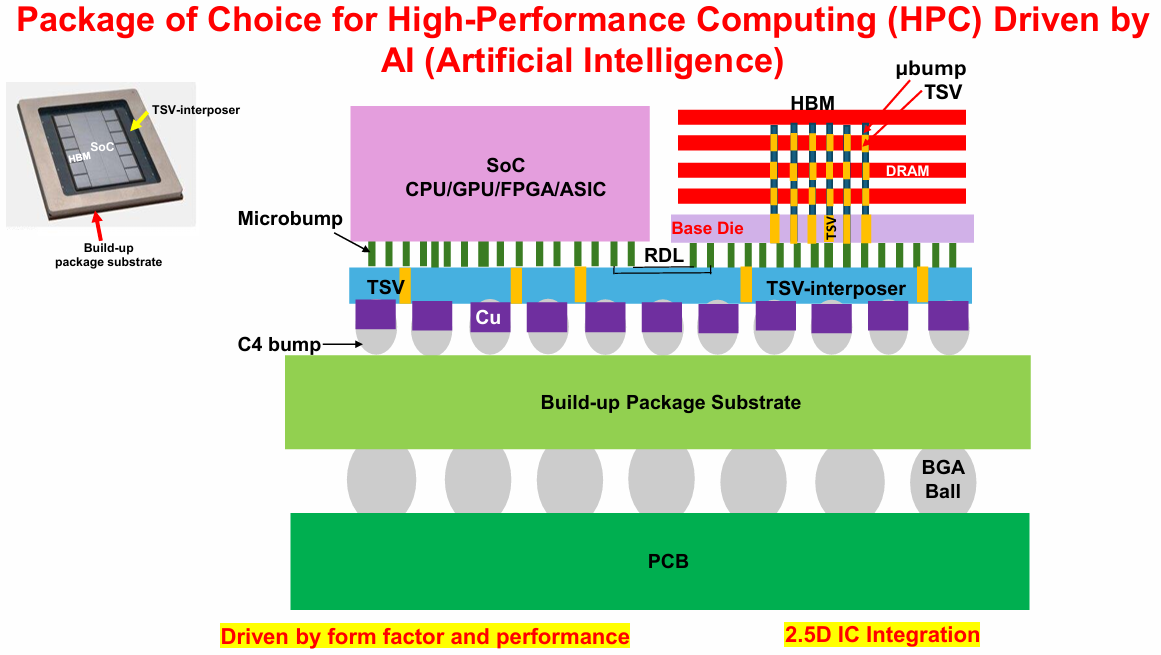
Figure 3. 2.5D Packaging of Choice. Source: Lau. J. (Unimicron) “Advanced Packaging for Chiplets, Heterogeneous Integration, and Co-packaging Optics” ECTC 2026
In the next section we will do a deep dive into the fabrication process of 2.5D and examine the fabrication process for each part. 2.5D is considered the package of choice for HPC due to its form factor and performance. For example, the NVIDIA H100 “Hopper” GPU uses this package and a cross section shows key features between the build-up package substrate and logic.
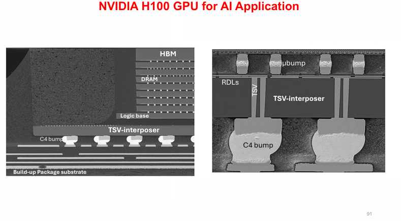
Figure 4. A Cross section of the H100 GPU with key package features. Source: Lau. J. (Unimicron) “Advanced Packaging for Chiplets, Heterogeneous Integration, and Co-packaging Optics” ECTC 2026
TSV Fabrication
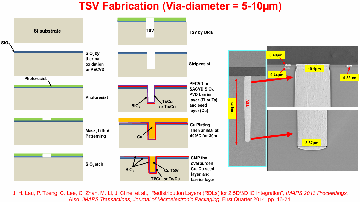
Figure 5. TSV Fabrication Process. Source: Lau. J. (Unimicron) “Advanced Packaging for Chiplets, Heterogeneous Integration, and Co-packaging Optics” ECTC 2026
A through-silicon via (TSV) transports signals and power completely through the thick structural floor (the raw Silicon Substrate). In CoWoS, the diameter is ~ 5-10um and the pitch is ~40-50um.
Lets go through the process steps:
- First, we start with standard lithography to add SiO2 on the Si surface that acts as the “hard mask” for TSV:
- Deposit SiO2 by thermal oxidation of Plasma-Enhanced Chemical Vapor Deposition (PECVD)
- Apply Photoresist
- Pattern with lithography through a photo mask
- Etch the SiO2
- After the SiO2 is deposited, the via hole is formed using Deep Reactive Ion Etching (DRIE). The most commonly used process is the Bosch process.
- After this hole is formed, it is filled with copper:
- An SiO2 layer is added with PECVD/Sub-Atmospheric CVD to act an an electrical insulator against Si and Copper
- Then, a barrier (Ti/Ta) and seed (Cu) added to prevent copper poisoning
- Then, the hole is filled with copper, annealed to stabilize the grain structure, and polished with CMP.
Important thing to note: The more power TSVs you add to feed a power-hungry GPU, the more you “choke” the horizontal routing channels available for the RDLs to connect the GPU to its HBM memory.
RDL Fabrication
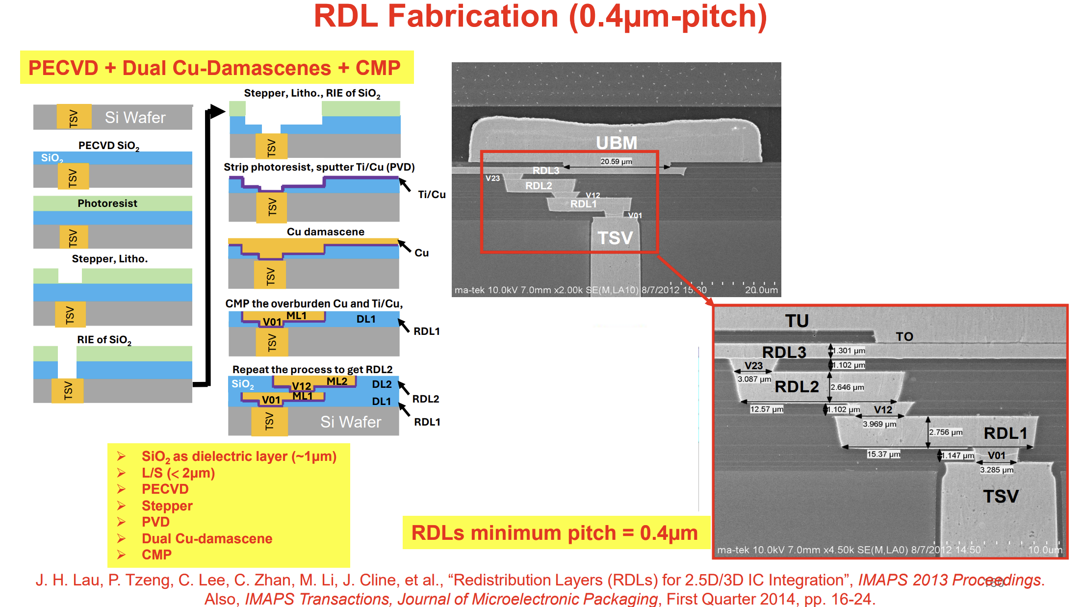
Figure 6. RDL Fabrication Process. Source: Lau. J. (Unimicron) “Advanced Packaging for Chiplets, Heterogeneous Integration, and Co-packaging Optics” ECTC 2026
Then the RDLs are fabricated on top of the TSV using Standard BEOL Processes using dual damascene. Dual damascene refers to etching both the via and horizontal line trench before adding any metal. Heres how it works:
- Form the via and M1 trenches with standard lithography. This is the same process as with TSVs: Deposit SiO2 with PECVD + photoresist on top, etch the photoresist then the oxide
- Line trenches with a thin Ti/Cu seed layer with PVD
- Overfill the whole trench with electroplated copper
- Polish the excess copper on the surface with CMP to give you a planar surface
Compared to standard packaging methods that limit pitch to 2-5um, this method can get down to 0.4um (at the time of writing this paper).
A passive silicon interposer typically features 4 to 6 BEOL metal layers on the front-side (top), and 2 to 4 coarser packaging RDL layers on the back-side (bottom).
As more layers are added, film stress is added. With HBM4, foundries like TSMC and UMC are actively extending front-side BEOL capabilities to 8, 9, or 10 layers to accommodate the massive explosion of traces.
Interconnect Options
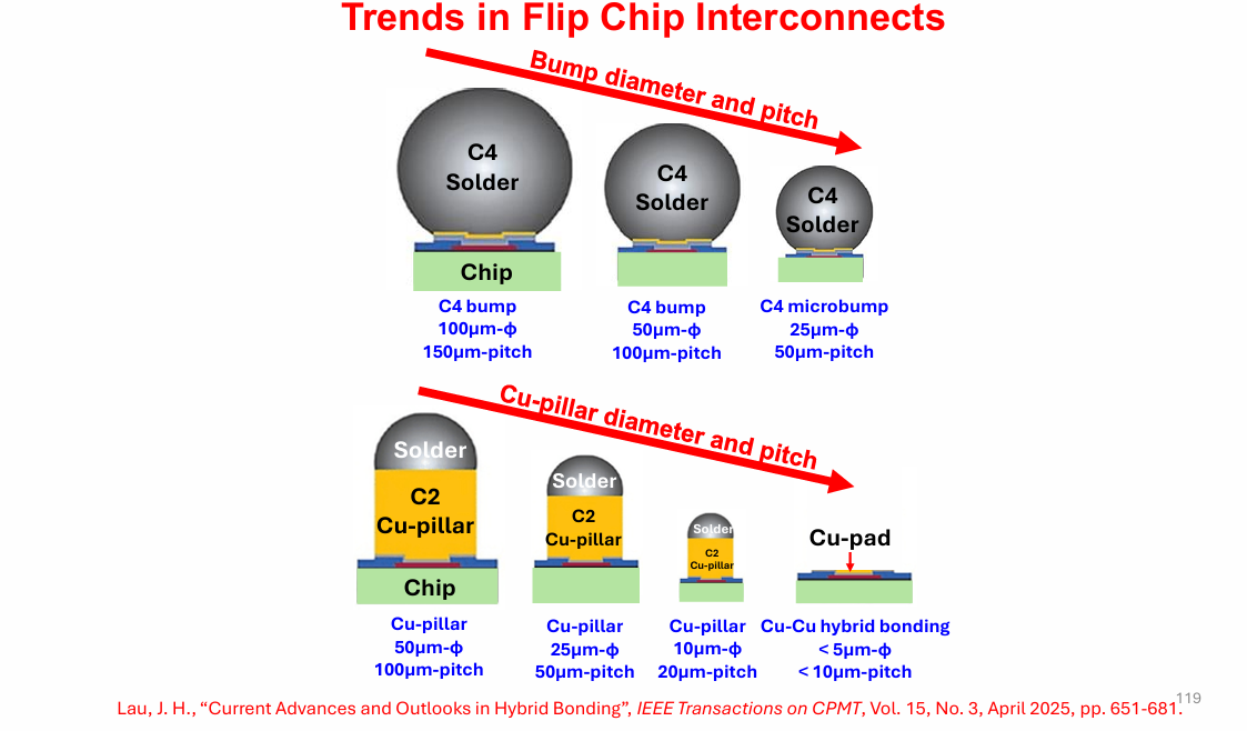
Figure 7. Bump Options. Source: Lau. J. (Unimicron) “Advanced Packaging for Chiplets, Heterogeneous Integration, and Co-packaging Optics” ECTC 2026
Bumps are formed by first forming an under/bump metallization with both a thin barrier layer (Titanium, tungsten, chromium) and seed layer (Copper/nickel). There are two major categories of bumps:
- C4 (Controlled Collapse Chip Connection):
- C4 bumps are great for macro power delivery and board-level packaging
- However, the pitch of C4 bumps are limited to 50-150um because they can cause “solder bridging” if they are too close
- C2 Pillar
- The actual solder is just a tiny cap sitting on top of a rigid, electroplated copper that does not melt during reflow
- These allow you to jam interconnects much closer together, but are much more expensive, primarily due to plating time of the Cu pillars
The other major option is Hybrid Bonding, which I’ll discuss at the end.
At higher current densities, both bump resistance and CTE affect reliability. I noticed a few posters at ECTC that demonstrate how a few small effects can magnify:
- Bumps further from the neutral point of a chip experience more deformation as substrate/chip area get larger
- The direction current flows into and out of the bump affects the equivalent resistance of the bump by a few percentage points
- The elemental composition at the bond interface can affect current density as well.
At higher current densities, these effects can lead to localized joule heating that can create “hotspots” and can increase the probability of failures.
Substrate Options
Silicon substrates are great for fabricating the fine pitch interconnect needed in between chiplets. However, silicon substrates are running into a few problems:
- They are expensive
- Fabrication is limited to major IDMs
- Substrates are running into photolithography reticle size limits
- Silicon everywhere is frankly overkill when the fine pitched interconnect is limited to specific areas in between chips.
After the paywall, I’ll discuss the following:
- Two alternative options to silicon: Glass and organic with bridges.
- Panels vs wafers, and why we didn’t do panels in the first place
- A brief history of hybrid bonding, the mechanism, and why its not widely adopted yet
⚠️ 付费墙提示:以上为免费公开部分。作者列出的后续章节(Glass Substrate 与 SeWaRe/凸点可靠性挑战、Panel or Wafer、Embedded bridge in Organic Substrate / TSMC CoWoS-L vs Intel EMIB-T、Hybrid Bonding 工艺步骤)均位于付费墙之后,本发布未包含。如需这些深度内容,请至原专栏订阅。
第二部分:解析(深度解读)
核心论点摘要
Chad 这篇更像「先进封装通识课」,用城市规画的类比把从 2D 到 3.5D 的封装谱系讲清楚,再以 TSMC 2.5D CoWoS 做一次完整拆解(TSV → RDL → 凸点)。几个值得记住的点:
- 封装即「城市规画」: rural=2D、suburb=2.1/2.3/2.5D、city=3D/3.3D/3.5D。封装的本质,是在「片上互连(纳米级)」与「板级走线(毫米级)」之间相差一个数量级的维度鸿沟上架桥。
- 2.5D 是当下 AI/HPC 的事实标准:H100「Hopper」即用此形态。2.1D/2.3D(ABF/PID 薄膜 RDL)是低成本替代,但不及 2.5D 的性能与密度。
- CoWoS 三件套拆解:
- TSV:直径 ~5–10µm、pitch ~40–50µm,Bosch 深硅刻蚀 + 铜填充 + CMP;关键洞见——给 GPU 喂电的 TSV 越多,留给 RDL 连 HBM 的「横向走线通道」越被「掐喉」。
- RDL:dual damascene,pitch 可做到 0.4µm(标准封装仅 2–5µm);被动硅中介层正面 4–6 层 BEOL、背面 2–4 层粗 RDL;HBM4 推动下 TSMC/UMC 正把正面 BEOL 推到 8/9/10 层。
- 凸点:C4(pitch 50–150µm,易桥连)vs C2 Cu Pillar(可更密但电镀时间长、贵);高频电流下 bump 电阻 + CTE 引发焦耳热「热点」,是可靠性隐患。
- 基板之痛引出下一波方向(付费段):硅基板贵、仅限 IDM、撞上光刻 reticle 尺寸上限、且「处处硅」属于过度设计——这正是玻璃基板、面板级、有机基板内嵌桥(CoWoS-L vs EMIB-T)、混合键合登场的理由。
关键概念解读
1. 谁是「总装」的责任人:fab 还是 OSAT? 作者点出一个产业级真问题:当混合技术(有机基板里的 bridge、LSI)出现后,最终封装集成该由 fab 还是 OSAT 负责,仍在激烈博弈。这恰好呼应 《CPO 最大的瓶颈:高良率测试》 里「测试与良率责任边界」的讨论——封装越集成,责任归属越模糊。
2. 2.5D 与「瓶颈移向先进封装」是同一叙事 本文的 2.5D 拆解,是 《AI 瓶颈正移向先进封装》 的「物理底座」:当算力瓶颈从 GPU 本身外溢到 chiplet 互连、HBM 带宽与封装走线,懂封装就等于懂了下一阶段的算力天花板。
3. CoWoS-L vs EMIB-T 的伏笔 免费段只抛出「有机基板内嵌桥」的方向,把 TSMC CoWoS-L 与 Intel EMIB-T 的正面对比留给了付费段。本站 《先进封装:Intel EMIB vs CoWoS》 已对这两者做过系统性拆解,正好补齐本文付费段的空缺——建议搭配阅读。
4. 三星 2.xD 的同构逻辑 本文讲「把光/内存/逻辑共封装」的谱系,与 《TSMC 领先 CPO,三星把第三颗芯片贴到 HBM 旁》 中三星 2.xD(把 HBM、logic、SiPh 共封进单一封装)是同一技术脉络的不同切面。
分层拆解表
| 维度 | 关键判断 | 投资/产业含义 |
|---|---|---|
| 谱系 | 2D→2.1/2.3D→2.5D→3D/3.3D/3.5D,2.5D 为 AI/HPC 当前标准 | 2.5D 产能(CoWoS)仍是近 2–3 年稀缺资源 |
| TSV | 直径 5–10µm、pitch 40–50µm,喂电 TSV 挤占 RDL 通道 | 高带宽 GPU+HBM 的互连密度受 TSV/RDL 双重约束 |
| RDL | dual damascene 至 0.4µm;HBM4 推正面 BEOL 至 8–10 层 | 中介层层数军备竞赛,利好 BEOL/电镀设备 |
| 凸点 | C4(粗、易桥连)vs C2 Pillar(密、贵);焦耳热热点 | 高密度下的可靠性/热管理是关键验证项 |
| 基板瓶颈 | 硅贵、限 IDM、撞 reticle 上限 → 玻璃/面板/桥/混合键合 | 玻璃基板、面板级封装是下一波材料与设备机会 |
风险提示
- 付费段信息缺口:玻璃基板(SeWaRe、凸点可靠性)、面板 vs 晶圆、CoWoS-L vs EMIB-T、混合键合工艺等深度内容位于付费墙后,本发布未覆盖;据此做判断时勿把免费段当成全貌。
- 集成责任未定:fab 与 OSAT 在混合封装最终集成上的权责仍博弈,可能拖慢新工艺量产节奏。
- 可靠性放大效应:CPO/高密度封装里,局部焦耳热、CTE 失配、bump 形变等小效应会被高电流密度放大,良率爬坡存在不确定性。
注:本文为 Silicon Co-Design 公开免费内容的整理与解读,所有专家观点与图示版权归原作者 Chad 及来源(John Lau / Unimicron,ECTC 2026)所有;付费段内容未包含,以上分析仅作产业研究参考。