Advanced Packaging: Intel's EMIB vs TSMC's CoWoS — 先进封装:Intel EMIB 对决台积电 CoWoS
整理 Austin Lyons (Chipstrat) 关于 AI 加速器先进封装的科普:reticle 上限如何催生 2.5D 封装、台积电 CoWoS 家族(S/R/L)与 Intel EMIB 的架构差异,并从成本、面板利用率、reticle 外扩展性、小片键合良率四维度对比 EMIB 与 CoWoS-L。英文原文 + 中文深度解读。
本文整理自 Austin Lyons / Chipstrat(chipstrat.com,Substack 专栏),原文发布于 May 12, 2026(标题原文:Advanced Packaging: Intel’s EMIB vs TSMC’s CoWoS)。 结构为 正文(英文原文)+ 解析(中文深度解读),方便中英对照阅读。 来源说明:内容经公开页面获取;本发布保留完整英文原文并附中文深度解读,仅作信息整理与学习用途,著作权归原作者所有,建议在原站支持作者订阅。 ⚠️ 本文为公开免费文章,已含完整正文;文末付费部分(三个前瞻情景、CoPoS 反驳、Amkor 二线来源等)仅作结构提示,未转载付费深解。
第一部分:正文(Original Article)
Advanced Packaging: Intel’s EMIB vs TSMC’s CoWoS
Is Intel’s EMIB better than TSMC’s CoWoS for AI accelerators? A primer on both, an honest look at the trade-offs, and where it goes from here.
Nvidia’s Rubin Ultra is going to be a huge chip. So huge that it likely takes four reticle-sized compute dies stitched together into one package.
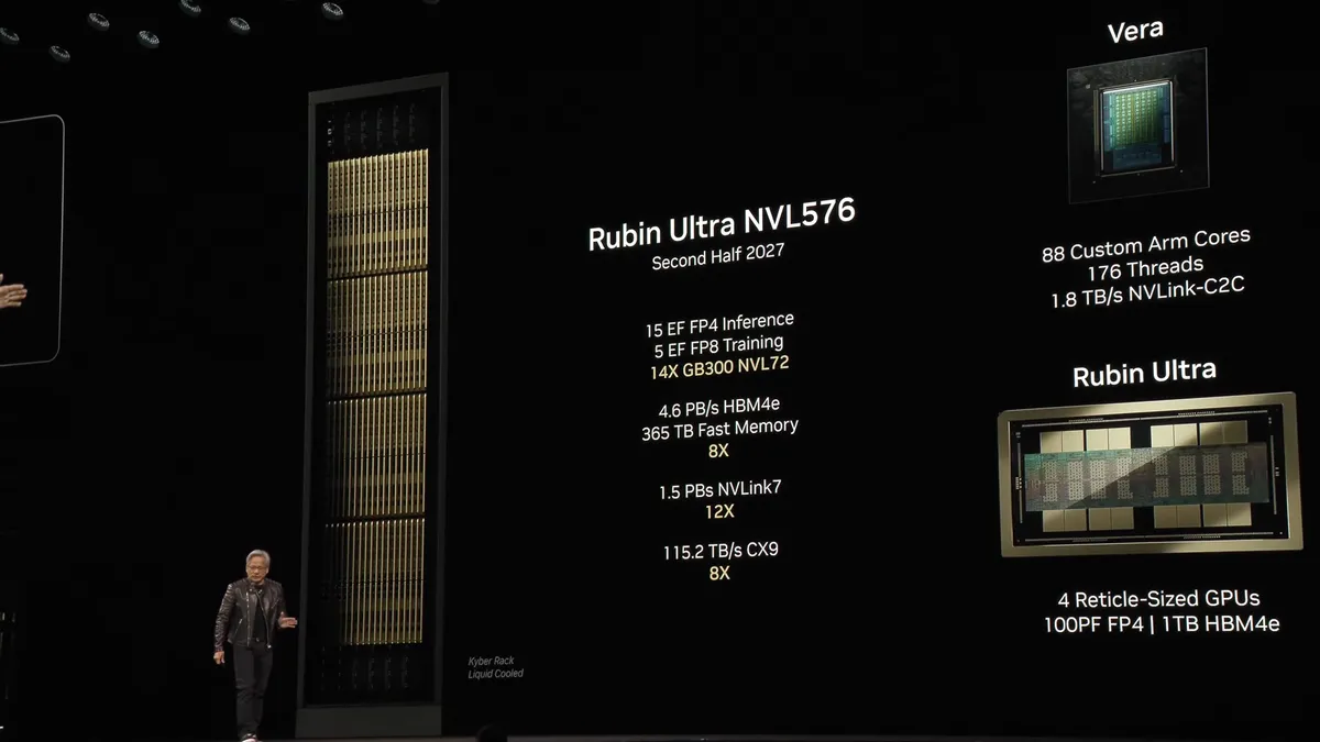
Well… allegedly. There are rumors of a warpage problem on the 4-die package, and chatter that TSMC is leaning on panel-level packaging (CoPoS) to deal with it, maybe even a fallback to a 2+2 config. Hold that thought.
So how do you connect four pieces of silicon together such that they behave electrically like a single chip? That’s the question of advanced packaging. And as AI accelerators keep getting bigger, the packaging itself is becoming the dominant cost variable in the bill of materials.
Today we’ll cover:
- A primer on 2.5D advanced packaging, and the reticle limit that started the whole story
- TSMC’s CoWoS family (CoWoS-S, CoWoS-R, CoWoS-L)
- Intel’s EMIB
- EMIB vs CoWoS-L
What is the reticle limit?
The way you make a chip more powerful, historically, has been to make it bigger. More transistors, more compute, more parallelism per die.
The ceiling on “bigger” is the reticle limit: the largest area a lithography stepper can pattern in a single exposure. About 26 mm × 33 mm, or roughly 858 mm².
NVIDIA’s H100 was already pushing the reticle. Blackwell broke through by stitching two reticle-sized compute dies together into a single GPU:
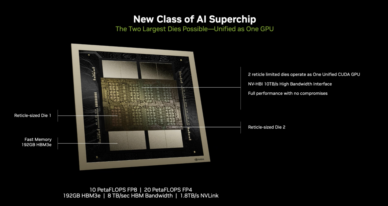
Once you cross that line (i.e. when one die isn’t enough) you need a way to physically connect multiple dies so they behave electrically like a single chip:
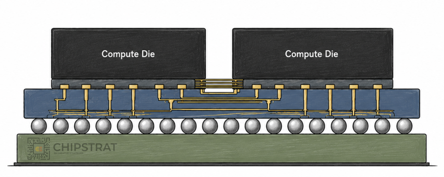
That’s advanced packaging. And as accelerator sizes grow, the cost of the packaging itself becomes a dominant economic variable.
What is 2.5D packaging, and why is it called that?
2D is one or more dies sitting directly on the organic substrate. No interposer, no bridge. Routing runs through the substrate itself.
That covers classic monolithic packages and chiplet designs where the dies talk through substrate traces. The constraint is density. Substrate pitch is coarse, so you get moderate die-to-die bandwidth, not the tight compute-to-HBM coupling AI accelerators need.
2.5D adds a passive silicon routing layer between the dies and the substrate. That can be a full silicon interposer, a silicon bridge embedded in the substrate like Intel EMIB, or silicon bridges inside an RDL interposer like TSMC CoWoS-L. It carries fine-pitch routing and sometimes TSVs, but no working transistors. It moves signals, it does not compute.
That is what makes tight compute-to-HBM coupling possible, and it is the dominant architecture in modern AI accelerators.
3D goes vertical. Silicon stacked on silicon — AMD 3D V-Cache, Intel Foveros, TSMC SoIC.
To get nitpicky: 2.5D with CoWoS-S is also technically “silicon on silicon”, but the interposer underneath is passive. Think of 3D as active on active and 2.5D CoWoS-S as active on passive.
HBM stacks are 3D internally, though they usually sit in a 2.5D package.
TSMC’s CoWoS family: three variants
Chip-on-Wafer-on-Substrate (CoWoS) is TSMC’s umbrella for 2.5D packaging. There are three commercially relevant variants. They differ mainly in how much silicon is used for interconnect.
CoWoS-S: full silicon interposer
The original. Entered production with Xilinx’s Virtex-7 2000T FPGA around 2011, where four FPGA slices were stitched together on a passive silicon interposer:
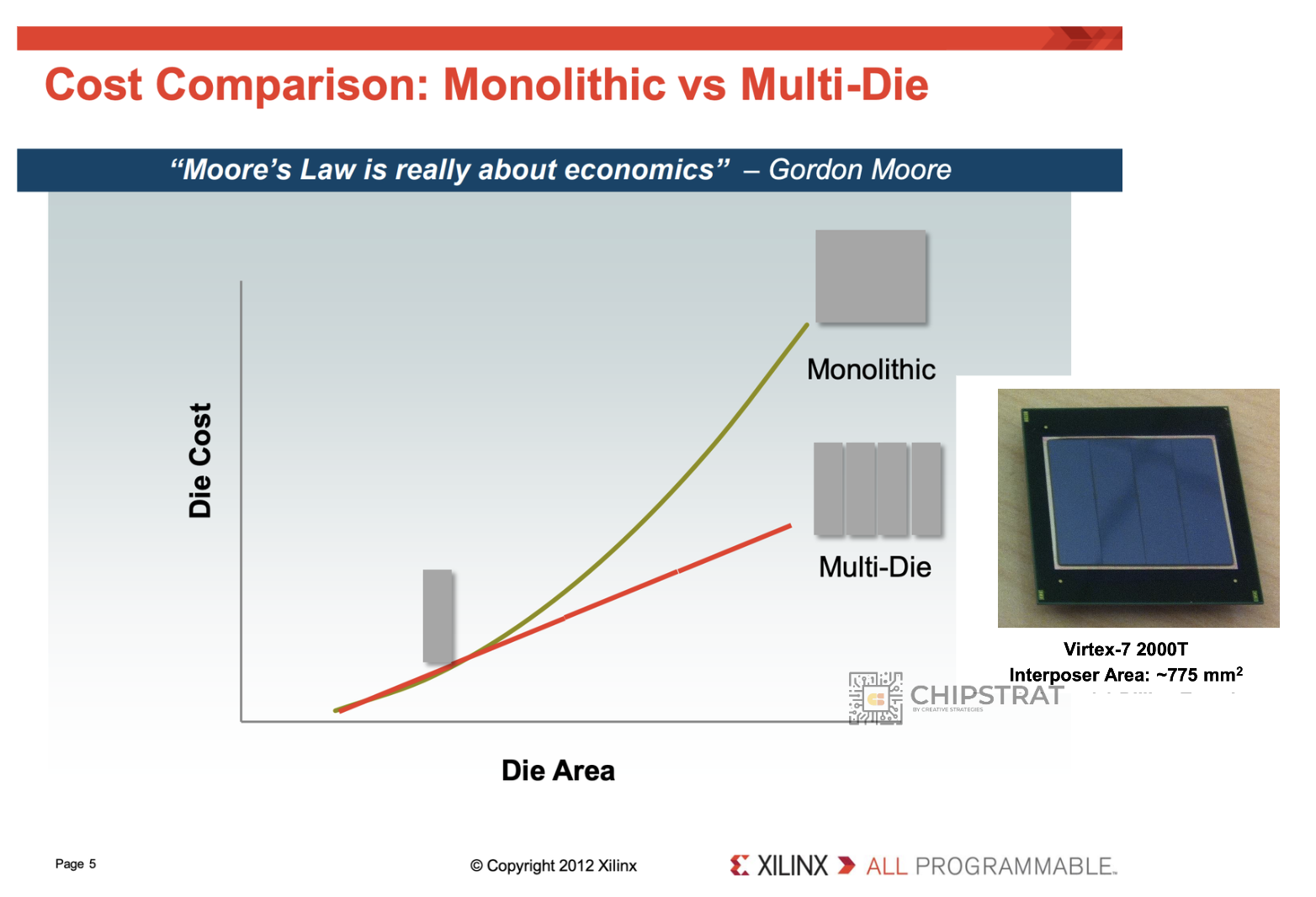
How it works:
- Multiple active dies sit on top of a large passive silicon interposer
- The interposer sits on the organic package substrate below
- The interposer carries fine-pitch metal routing for dense lateral interconnect, plus Through-Silicon Vias (TSVs) that route signals and power vertically down to the substrate
Important nuance: the interposer is not a “logic chip” in the compute sense. It’s processed on a mature silicon node optimized for routing density and TSV formation, not transistor performance. No logic, no transistors doing work on it.
Think of it as a tiny circuit board made out of silicon. Same job as a PCB, just at lithography pitch instead of PCB pitch, with several fine-pitch metal layers plus a forest of vertical vias.
Electrically, this gives you tens of thousands of short, fine-pitch interconnects between neighboring dies, at far lower latency and power than routing the same signals through an organic substrate.
Here’s what that original Xilinx example looked like:
HBM made this silicon interposer the default approach for flagship AI parts. The HBM interface is too wide and too dense for conventional packaging. Once GPUs adopted HBM (notably AMD’s Fiji / Radeon R9 Fury X), large silicon interposers became standard across every high-end AI accelerator that uses HBM:
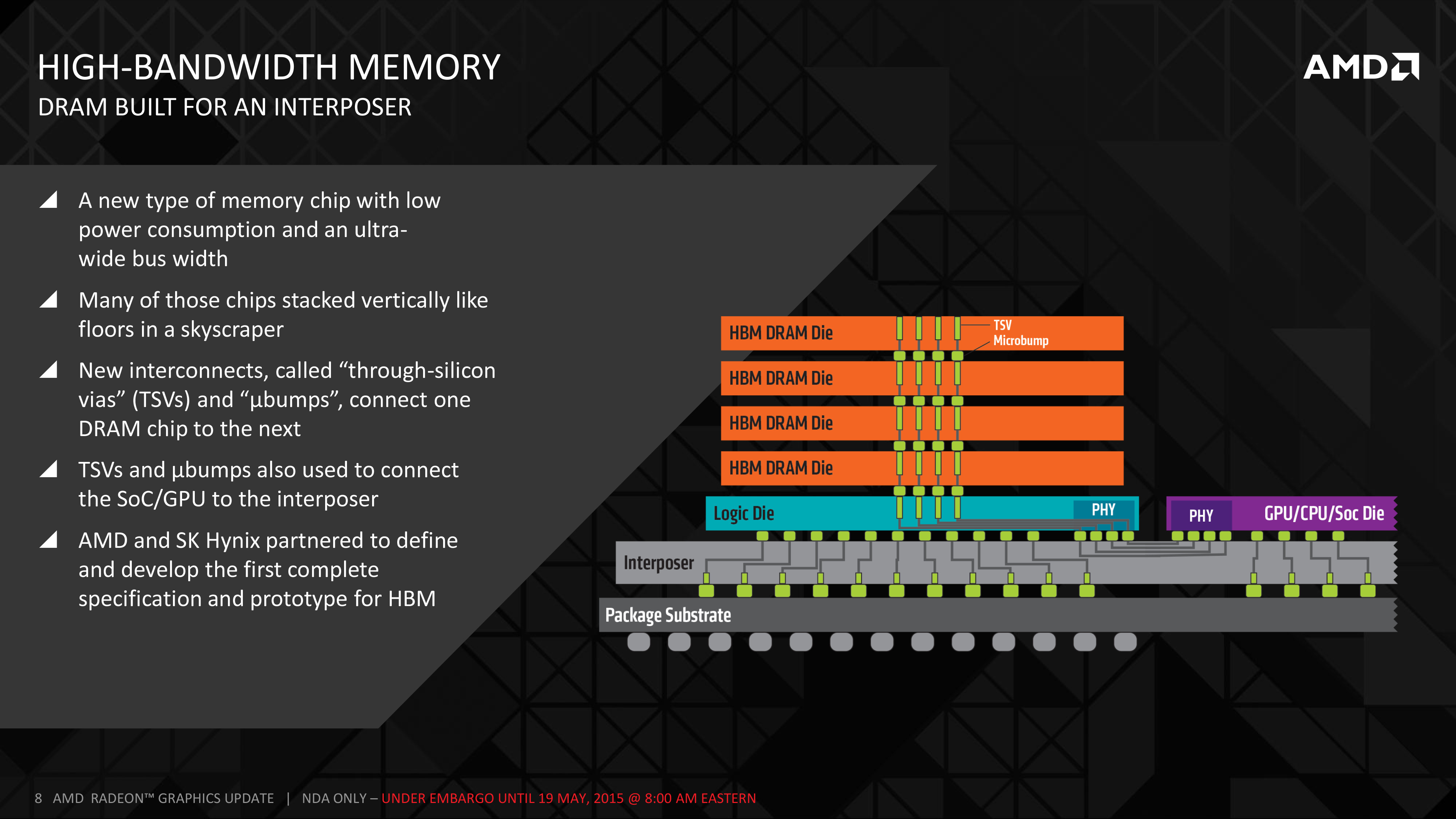
There’s an economic problem though. The silicon wafer is being consumed for routing, not compute. That’s expensive. As HBM stack counts grow and compute reticle counts grow, the per-package silicon bill grows right alongside them.
CoWoS-R: organic RDL interposer
TSMC’s response to the silicon interposer cost is to build the routing in Redistribution Layers (RDL) of organic material instead of silicon:
This is cheaper, but isn’t a silver bullet. Organic processes have wider lithographic tolerances than silicon. Trace pitch widens, layer count climbs, and the assembly can’t match the bandwidth density that an HBM-to-GPU interface demands.
Thus, CoWoS-R is useful for cost-sensitive products that don’t need the densest die-to-die interconnect. It cannot carry flagship AI accelerator workloads on its own.
Trade-offs!
CoWoS-L: local silicon bridges in an interposer
TSMC’s current frontier, which places small silicon bridges only where you need high-density routing (compute-to-compute, compute-to-HBM). Use cheaper organic RDL material everywhere else on the interposer.
The bridges sit inside the interposer. The interposer is then attached to the package substrate as one large piece.
This is the TSMC architecture used for Blackwell-class accelerators.
The move is elegant balancing of trade-offs, with silicon where you need bandwidth, organic where you don’t. Beautiful in principle. The catch is that you’ve still got a separate interposer to build (an RDL carrier with those silicon bridges embedded in it), and then you have to dice it and attach the whole thing onto the package substrate. Two pieces, two attach steps.
Intel’s EMIB
Embedded Multi-die Interconnect Bridge (EMIB) shares CoWoS-L’s central insight (silicon only where you need it) but resolves it very differently.
EMIB skips the interposer entirely. The silicon bridges are embedded directly into the organic substrate of the package:
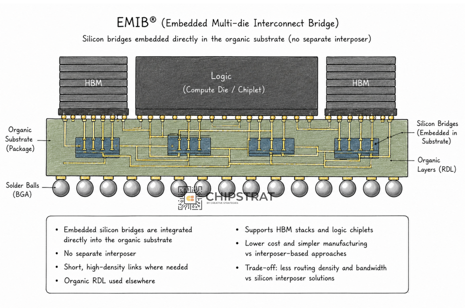
Here’s a cleaner version from Intel’s foundry blog:
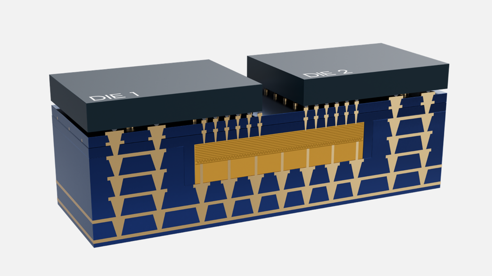
Note that EMIB has only two layers. Dies and substrate.
EMIB-T and EMIB-M
Worth noting quick: Intel has next-iteration variants. EMIB-T adds Through-Silicon Vias through the embedded bridges themselves, which lets power and high-speed signals flow vertically through the bridge, not just laterally. HBM-heavy designs increasingly need this. EMIB-M integrates MIM (Metal-Insulator-Metal) capacitors into the bridge for on-package power decoupling.
Both are direct descendants of the same “embedded in the substrate” architecture. Worth a watch on Intel’s recent EMIB-T/M explainer:
EMIB vs CoWoS-L, side by side
So EMIB and CoWoS-L are both bridges right? Which is better?
- EMIB: silicon bridges embedded directly in the organic substrate. One piece, one attach step.
CoWoS-L: silicon bridges embedded in an RDL interposer; that interposer then attached to the package substrate. Two pieces, two attach steps.
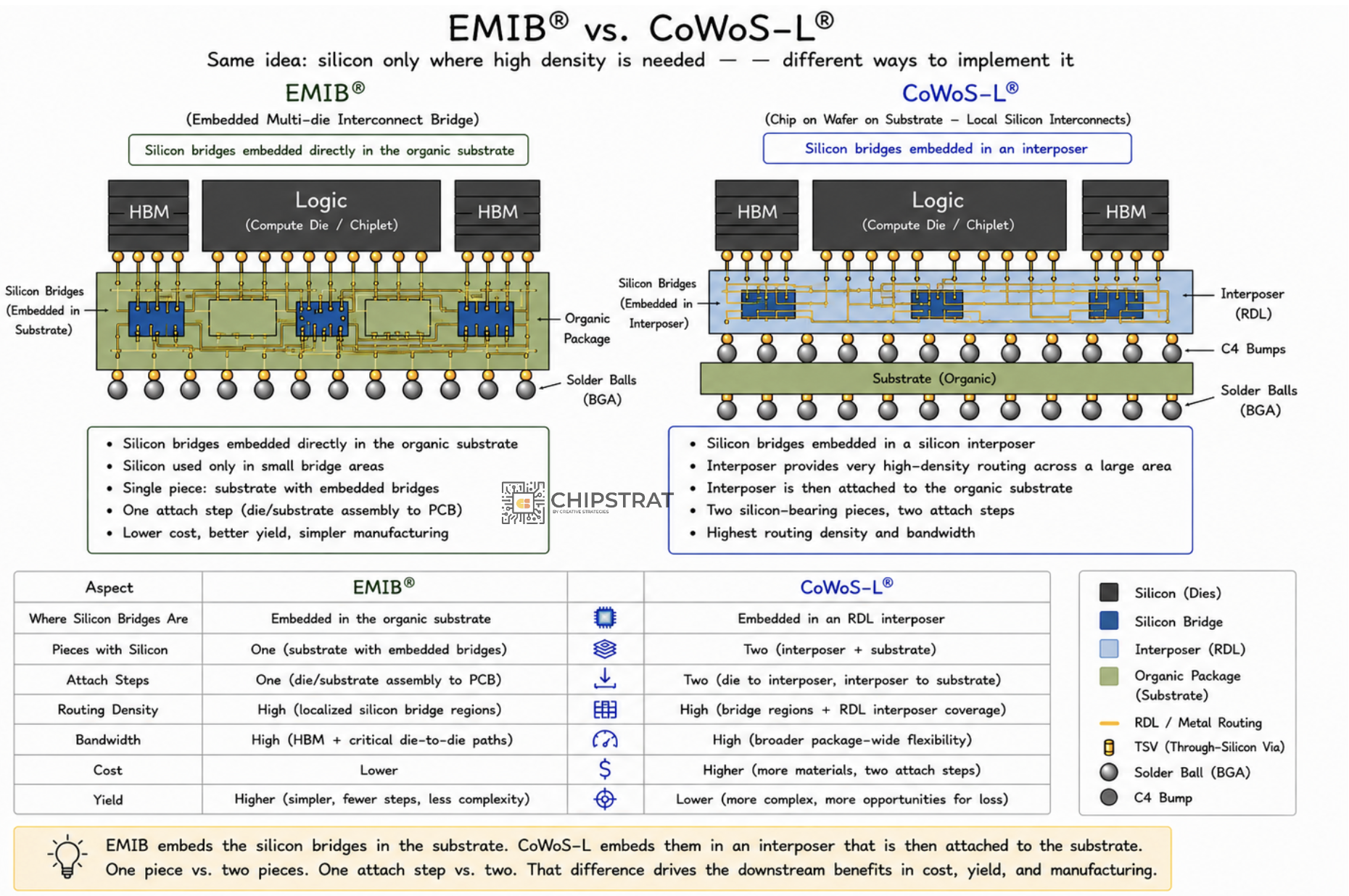
That one difference leads to these value props:
1. Cost
EMIB doesn’t have a separate interposer to amortize at all. The silicon bridges are small dice embedded in a package substrate that already exists.
Let’s be precise about what’s being compared here. Every flip-chip package, EMIB or CoWoS, sits on a panel-made organic substrate. CoWoS-L additionally builds and attaches a separate interposer (an RDL carrier with small silicon bridges embedded in it) between the dies and that substrate. That extra interposer, plus the extra process steps and the extra attach, is the cost difference. And in current-gen CoWoS-L that interposer is built in round-wafer format, so the panel-vs-wafer waste from the next section applies to it too. EMIB just doesn’t have any of it. The bridges are cheap because they’re tiny, and you get thousands per wafer.
Process steps eliminated:
- Interposer build
- Interposer dicing
- The interposer-to-substrate attach
That’s three places where cost and yield could go wrong, but won’t for EMIB, because they don’t happen.
2. Panel utilization
This is a big one, even if it sounds boring, and it matters more the further along the roadmap we go.
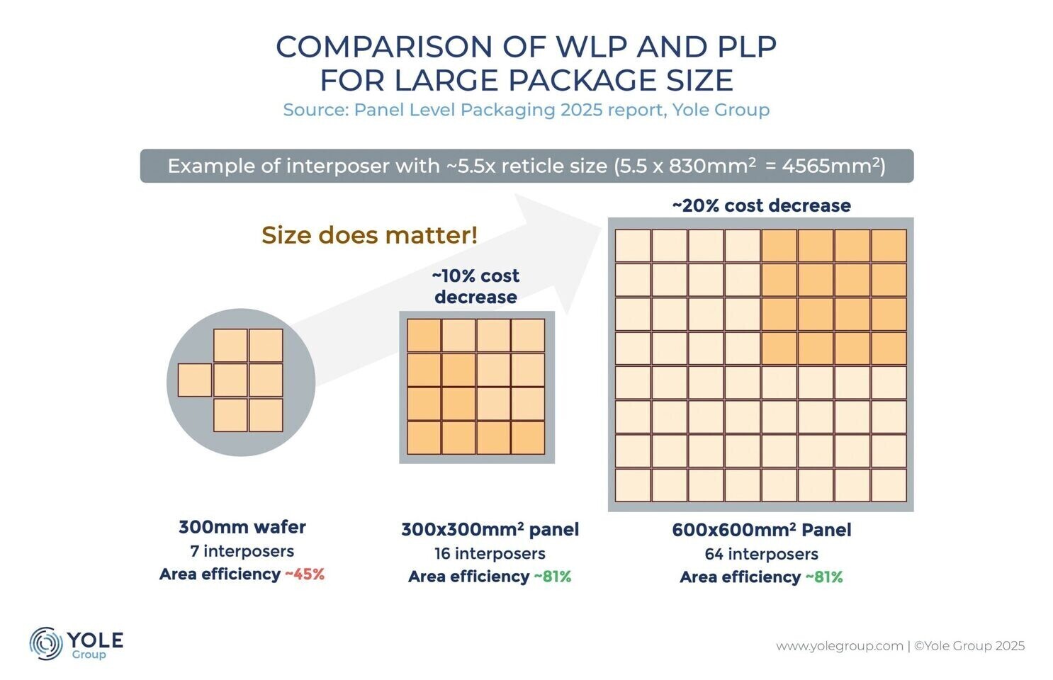
Silicon interposers are cut from 300 mm round wafers. Packages are rectangles. Rectangles on round wafers leave significant edge waste, and the waste fraction grows with interposer size. The bigger the interposer, the more wafer area you throw away at the edges.
Substrates use rectangular panels (a common size is roughly 510 mm × 515 mm). Rectangles tiled into a rectangle. The math is much friendlier.
Intel cites approximately 60% wafer utilization for interposer-class CoWoS versus approximately 90% panel utilization for EMIB:
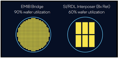
That’s the cost headline. On a flagship part with a multi-reticle package, you’re looking at a substantial cost-of-goods delta before counting anything else.
And remember the Rubin Ultra rumor from up top? The fix that keeps coming up is CoPoS (Chip-on-Panel-on-Substrate), which is TSMC moving its advanced packaging off round wafers and onto rectangular panels. CoPoS isn’t EMIB. TSMC keeps its carrier-and-RDL approach; it just runs it on a panel. But the package got too big for a round wafer, and the fix is panels. Intel’s package substrate was a rectangle from the start.
3. Scalability past the reticle limit
This one is just geometry.
A reticle is roughly 26 mm × 33 mm = 858 mm².
- A 5-reticle complex (think Blackwell-scale, roughly Rubin-ish): ~4,290 mm², or about 43 cm².
- A 14-reticle ceiling: ~12,000 mm².
A 300 mm wafer has π × (150 mm)² ≈ 70,686 mm² of total area, and the usable rectangular yield is meaningfully smaller once you account for edge waste and dicing kerf. At 14-reticle interposer sizes, you’re approaching one interposer per wafer.
One. Interposer. Per. Wafer.
At that point the interposer absorbs the entire cost of the wafer. Packaging cost stops scaling and starts cliff-diving in the wrong direction.
EMIB stretches in X and Y across say a 515 mm × 510 mm panel (≈ 263,000 mm² of usable area). The “one interposer per wafer” problem doesn’t arise.
So the cost curves diverge. The larger the package, the wider EMIB’s margin gets.
And packages keep getting larger every generation.
4. Yield through smaller bonded pieces
Bonding a single 5-reticle silicon interposer onto a substrate is a tough operation. You’re moving a ≈ 43 cm² silicon piece through reflow, and silicon and substrate have different coefficients of thermal expansion. Warpage at that size is a yield-limiting problem. Remember that alleged Rubin Ultra issue above?
EMIB attaches dies individually to the substrate. Each attach is small, locally thermally controlled, and decoupled from the others.
Small-piece bonding is inherently higher-yield than big-piece bonding. The yield advantage compounds with package size for the same geometric reason the cost advantage does.
That’s the case for EMIB on the merits. For paid subscribers: three forward scenarios with my thoughts, the “TSMC will just do CoPoS” pushback, the Amkor partnership that adds a second source for EMIB (and why it’s a 2028 story, not a 2026 one), and what it all means for how you read Intel Foundry’s hand. If those tickle your fancy, keep reading.
第二部分:解析(深度解读)
一、这篇文章为什么重要
Austin Lyons 这篇 Chipstrat 文章,是少数把「先进封装」这件事用「工程师能读懂、投资者也能跟上」的方式讲清楚的基础读物。它不直接谈股票,却把 2026 年整个 AI 硬件叙事里最被低估的一层——封装(packaging)——的物理边界讲明白了。
对站内的 CPO / 硅光系列读者来说,这篇文章补上了「光」之前的那块拼图:在光 I/O 进入封装之前,电 die 之间怎么连、为什么非连不可、以及连的成本由谁决定。它和本站已经发布的 台积电 CPO 领先、三星为第三芯片 形成互补:那篇讲「光往封装里走」,这篇讲「die 在封装里先怎么摆」。
二、核心论点拆解
| 概念 | 原文要点 | 投资 / 产业含义 |
|---|---|---|
| Reticle 上限 | 单次曝光最大约 26×33 mm ≈ 858 mm²;H100 已顶到上限,Blackwell 用双 die 拼接跨过 | 单 die 做大已到物理顶,AI 加速器只能「拼 die」→ 封装成为必选项 |
| 2.5D 的本质 | 在 die 与有机基板之间插入一层「无晶体管的被动硅布线层」(全 interposer / 嵌入 bridge / RDL) | 实现 tight compute-to-HBM 耦合的唯一可行架构,是现代 AI 加速器的主流 |
| CoWoS 三变体 | S=全硅 interposer(贵)、R=纯有机 RDL(便宜但带宽密度不够)、L=局部硅桥 + RDL(Blackwell 级主力) | L 是当前旗舰首选;S 烧晶圆面积、R 撑不住 HBM 带宽 |
| EMIB 的巧思 | 完全跳过 interposer,把硅桥直接埋进有机基板,只有 die + 基板两层 | 少一次 interposer 制造 + 切割 + 贴装,省三步成本与良率风险 |
| EMIB vs CoWoS-L | 前者一片一层一贴;后者硅桥在 RDL interposer 内、再贴到基板,两片两贴 | 这一个结构差异推导出成本、面板利用率、reticle 外扩展、小片键合良率四组差异 |
一句话:两种方案都认同「只在需要高带宽处放硅」,但 EMIB 把桥埋进基板、CoWoS-L 把桥放在 RDL 载板里再贴基板——这一个位置差异,拉开了一整套成本与良率账。
三、关键概念 / 技术解读
1. Reticle 上限是整篇文章的物理起点。 光刻机单次曝光能投出的图案上限约 858 mm²(略小于一张信用卡)。当 AI 加速器想要比这更大时,唯一办法是不再「印一颗大芯片」,而是把多颗小 die(chiplet)拼成一颗「表现得像一颗巨芯片」的封装。这就是先进封装存在的根本原因——不是工艺偏好,是光学几何的硬约束。
2. 2.5D / 3D 的边界。 2.5D 是在 die 与基板间加一层「无晶体管、只走线」的被动硅(全 interposer、Intel EMIB 那种嵌在基板里的桥、或 CoWoS-L 那种 RDL 里的桥)。它不含工作晶体管,只搬运信号。3D 才是硅叠硅(AMD 3D V-Cache、Intel Foveros、TSMC SoIC)。HBM 内部是 3D,但通常躺在一个 2.5D 封装里。原文一句很妙:3D = active on active,2.5D CoWoS-S = active on passive。
3. CoWoS 家族的三档取舍。 S 用一整片大硅 interposer,布线密度最高但最贵(烧的是真晶圆面积);R 改用有机 RDL,便宜但线宽/层数受限,撑不住 HBM↔GPU 的带宽密度;L 是 TSMC 当前主力——只在 compute-to-compute、compute-to-HBM 处放小硅桥,其余用便宜 RDL。优雅,但代价是「仍要多造一片 RDL 载板、再切割、再整片贴到基板上」(两片两贴)。
4. EMIB 的核心差异。 EMIB 直接把硅桥埋进有机基板,整包只有 die + 基板两层。由此省掉 interposer 制造、interposer 切割、interposer→基板贴装三步——这三步既是成本点也是良率风险点,EMIB 直接「没有这一步」。衍生变体 EMIB-T(桥内加 TSV,让电源与高速信号能纵向穿过桥,而非只能横向走)对 HBM 重负载设计越来越重要;EMIB-M 在桥内集成 MIM 电容做片上电源去耦。
5. 四组对比的实质。
- 成本:EMIB 没有独立 interposer 要摊薄;CoWoS-L 多一片 round-wafer 格式的 RDL 载板,面板 vs 晶圆的边角废料也落在它头上。
- 面板利用率:硅 interposer 从 300 mm 圆晶圆切矩形,越大边角 waste 越严重;基板用矩形面板(约 510×515 mm)。Intel 称 interposer 级 CoWoS 约 60% 晶圆利用率 vs EMIB 约 90% 面板利用率。
- reticle 外扩展性:到 14-reticle(≈12,000 mm²)时,一片 300 mm 晶圆几乎只够切一个 interposer——「One interposer per wafer」,封装成本断崖式恶化;EMIB 在 515×510 mm 面板上横向铺开,不存在这个问题。
- 小片键合良率:5-reticle 整片硅 interposer 回流时,硅与基板 CTE 不同 → warpage 是良率杀手(回想上面 Rubin Ultra 翘曲传闻);EMIB 逐颗小 die 独立贴装,局部温控、互不影响,小件键合天然高良率。
四、与本站其他文章的链接
- 台积电 CPO 领先、三星把第三颗芯片贴到 HBM 旁 —— 本文讲「die 在封装里先怎么摆」,那篇讲「光 I/O 下一步怎么进封装」,是同一赛道的上下游。
- CPO 最大的瓶颈:高良率测试 —— 与本文「warpage / 大件键合良率」直接呼应:封装越大,翘曲与良率越成为产业瓶颈。
- CPO 为什么变得不可避免 —— 从电互联跨向光互联的同一叙事链。
五、行业 / 投资意义
- 封装是 AI BOM 里越来越主导的成本变量。 当单 die 撞上 reticle 上限、加速器只能 chiplet 化,封装(而非裸芯片本身)成为「能不能造出来、造多贵」的决定层。这与本站反复强调的「瓶颈正从前道移向后道」完全一致——先进封装的 AI 瓶颈正在移向日本三家公司 那篇把这条线索推向了材料层。
- EMIB 不是「性能优于 CoWoS」,而是「可得性 / 二线来源」之争。 本文明确说两者测的是不同东西:Intel 强调去掉晶圆级步骤、缩短周期、无 reticle 尺寸上限;TSMC 强调能做出业界最大封装。真正的分野不在微米,而在产能分配——当 NVIDIA 拿走约 60% CoWoS 产能、前三大客户锁定 85%+,其他人都去拥抱 EMIB 做第二来源。
- CoPoS 是 TSMC 的「用面板救晶圆」回应,不是 EMIB 的继任者——它保留 carrier+RDL,只是搬到矩形面板。这反而印证了 EMIB「基板本来就是矩形」的结构优势。
- 明确点名的方向性标的:Intel(EMIB / EMIB-T 阵营)、台积电(CoWoS 家族)、AMD(Rubin Ultra 多 die 封装的需求侧)、以及 Amkor(为 Intel 外包 EMIB 组装、为 TSMC 外包 CoWoS 的 OSAT 二线来源)。
六、风险提示
- 本文为公开免费科普,付费深解未转载。 文末三个前瞻情景、对「TSMC 会直接做 CoPoS 就赢了」的反驳、Amkor 二线来源(为何是 2028 而非 2026 故事)等均在付费墙后,相关定量判断请以原站付费内容为准。
- 架构之争 ≠ 性能之争。 原文反复强调 EMIB 与 CoWoS-L 不在同一维度比性能,投资上不能简单推导「EMIB 赢 → Intel 赢」。真正变量是产能可得性与认证周期。
- warpage 是贯穿全文的良率风险。 大尺寸整片 interposer 回流翘曲是 CoWoS 路线的物理软肋,也是 Rubin Ultra 传闻中 4-die 封装问题的根源;这同时是 CPO 测试瓶颈 的底层成因。
- 面板化(CoPoS / FOPLP)仍在早期。 TSMC 的 CoPoS 量产时间有 2028–2030 的不同说法,uniformity 与 warpage 是主要技术障碍,不能把「面板化」当作已兑现的确定性。
以上解读基于原文信息整理,不构成投资建议。