人造规范场下的无色散耦合调控:750 nm 间距密集波导阵列与任意分光比耦合器
Opto-Electronic Advances 论文精读:上科大团队用人造规范场(正弦轨迹调制)叠加波导宽度失配,在 SOI 上做出中心距 750 nm 的半波长间距密集波导阵列,C 波段实测串扰低于 −20 dB;同一机制反过来把耦合色散抵消,得到 60:40 / 70:30 的无色散分光器,并集成出 FoV 120°×14.5°、旁瓣低于 −17 dB 的二维光学相控阵。含英文原文完整转载(7 图 5 式)与中文结构化解读,其中我逐项复算了 Eq. (2) 的 Bessel 论证——原文把 a 定义式里的折射率标为衬底折射率,但数值自洽要求它是模式有效折射率(≈2.44)。
来源:Opto-Electronic Advances(中国科学院光电技术研究所主办,开放获取期刊,CC BY 4.0) 论文:Li T, Zhang H, Sun YH, Xu XC, Xu T, Zou Y. Dispersionless coupling control enabled by artificial gauge fields for dense waveguide arrays and arbitrary-ratio power splitters 作者单位:上海科技大学信息科学与技术学院;哈尔滨工业大学可调谐激光技术国家重点实验室;南京大学固体微结构物理国家重点实验室 原文:DOI 10.29026/oea.2026.260026 | 收稿 2026-02-25 | 接收 2026-04-30 | 在线发表 2026-06-02 | Opto-Electron Adv 9, 260026 (2026)(early view 版本,后续将编入正式期号) 转载说明:第一部分为英文原文完整转载,含全部 7 张配图与全部 5 个公式,仅统一数学记号、段落层级与图表编号格式;版权归原作者,原文以 CC BY 4.0 许可发布。第二部分为独立撰写的中文结构化解读,其中的核算、质疑与边界判断属解读者观点,不代表原作者立场。 ⚠️ 补充材料未含:原文的 Supplementary Sections 1–10 与 Supplementary Table S3 单独发布于期刊网站,不包含在正文 PDF 内。本文转载仅覆盖正文;凡依赖补充材料的论断,我在解读部分逐条标注,不做推测性补全。
第一部分:正文(Original Article / 英文原文)
Abstract
Evanescent coupling is central to integrated photonics, enabling essential functions such as power splitting, routing, and beamforming, yet it also fundamentally limits photonic integration density through crosstalk and strong wavelength dispersion. Achieving broadband suppression and control of coupling in densely packed waveguide arrays remains a long-standing challenge. Here, we present an artificial gauge field (AGF)-based strategy that enables both wavelength-insensitive coupling suppression and dispersionless, arbitrary-ratio power splitting on a silicon-on-insulator platform. By jointly engineering waveguide trajectory modulation and propagation-constant mismatches introduced through non-uniform waveguide widths, we realize a half-wavelength-pitched dense waveguide array with a center-to-center spacing of 750 nm, far below conventional coupling-limited separations. The resulting array exhibits broadband crosstalk suppression below −20 dB over a 100-nm wavelength range (1500–1600 nm) with negligible excess loss. In parallel, we demonstrate AGF-enabled directional couplers with colorless and programmable splitting ratios, achieving wavelength-independent power division across the same bandwidth. Leveraging these near-dispersionless couplers, we construct a broadband Gaussian-weighted waveguide array and experimentally realize a two-dimensional optical phased array with a field of view of 120° × 14.5° and sidelobe levels below −17 dB. Our work establishes a scalable framework for broadband coupling control in ultra-dense photonic circuits, opening new opportunities for compact optical phased arrays, photonic delay lines, and high-capacity space-division multiplexing systems.
Keywords: artificial gauge fields; waveguide; integrated photonics
1 Introduction
Coupling is a fundamental optical phenomenon that underlies the operation of a broad range of photonic devices1. It arises from the interaction of the evanescent field of guided modes with neighboring waveguides, enabling controlled energy transfer for power splitting, wavelength routing, and other essential functionalities2−4. Evanescent coupling is characterized by two key features: coupling strength that increases rapidly as the separation between waveguides decreases, and strong wavelength dependence arising from both material and geometric dispersion. This mechanism forms the physical basis of many on-chip components in modern integrated photonics5−9. However, unintentional coupling between adjacent waveguides can introduce crosstalk and excess propagation loss, ultimately constraining device performance and limiting integration density10,11. In dense photonic circuits, the minimum allowable waveguide spacing is often dictated by coupling-induced crosstalk. Reducing this spacing is particularly critical for footprint-intensive components such as optical delay lines, as well as for enhancing the field of view (FoV) in optical phased arrays (OPAs)12−17. Despite its importance, suppressing coupling in tightly packed waveguide arrays remains challenging due to the inherently weak optical confinement in dielectric waveguides18. Recent studies have demonstrated that carefully engineered waveguide trajectories can achieve near-complete coupling suppression, highlighting the potential of artificial gauge field (AGF) engineering for high-density photonic integration19−21. Nevertheless, such approaches are highly sensitive to geometric dispersion, which restricts their operational bandwidth and precludes broadband, zero-crosstalk operation in straight, densely packed waveguide arrays22.
At the same time, achieving broadband control over evanescent coupling remains a longstanding challenge. Devices based on conventional directional coupling typically exhibit pronounced wavelength dependence, resulting in narrowband operation that becomes increasingly restrictive in high-density photonic architectures23,24. Yet broadband, wavelength-insensitive coupling is essential for applications such as wavelength-division (de)multiplexers and wavelength-steered OPAs25−27. Developing a robust strategy for arbitrary and broadband coupling control is therefore of critical importance. Notably, AGF engineering offers unique opportunities for tailoring coupling dispersion, enabling compensation of the intrinsic wavelength dependence associated with evanescent-field interactions19.
Here, we present an AGF-based coupling manipulation strategy that enables dispersionless and arbitrary on-chip coupling control on a silicon-on-insulator (SOI) platform. Specifically, we demonstrate both a broadband coupling-suppressed dense waveguide array with half-wavelength-pitch and dispersionless power splitters with programmable splitting ratios as depicted in Fig. 1(a). The dense waveguide array consists of multiple non-uniform subarrays with a center-to-center spacing of 750 nm—significantly below the conventional coupling-limited separation. By jointly exploiting propagation-constant mismatches induced by waveguide-width variations and carefully designed trajectory modulations, we achieve strong and broadband suppression of coupling across the entire array. Experimental measurements show crosstalk below −20 dB over a wavelength range from 1500 to 1600 nm. In addition, we experimentally realize an AGF-enabled near-dispersionless coupling mechanism that provides arbitrary coupling strength independent of wavelength. By cascading these near-dispersionless couplers to generate a broadband Gaussian channel-intensity distribution, and combining them with the half-wavelength-spaced dense array, we demonstrate beam steering with a 120° × 14.5° FoV and a sidelobe level (SLL) below −17 dB at 0°. Our approach offers a scalable route to dramatically increase photonic integration density while maintaining low crosstalk and broadband functionality. It enables substantial reductions in on-chip footprint and provides a powerful framework for enhancing device performance in applications such as OPAs, photonic delay lines, and ultra-dense space-division multiplexing systems.
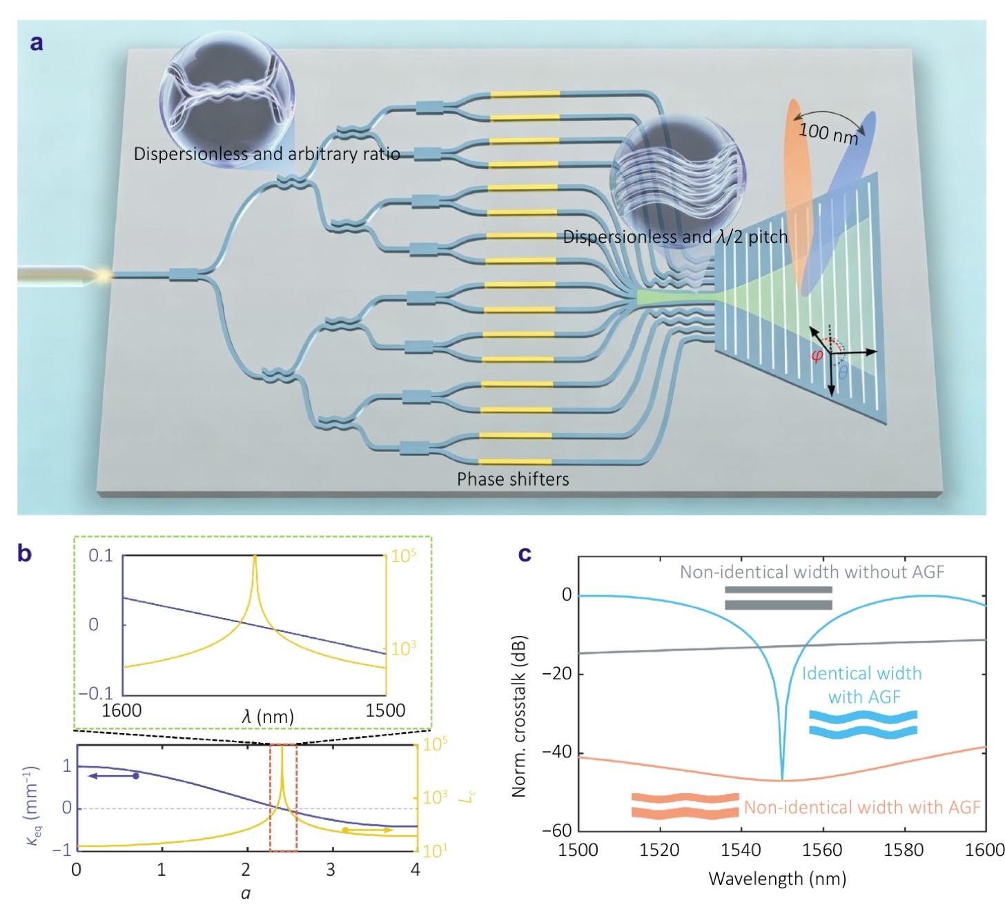
原文 Fig. 1 图注:Dispersionless coupling control enabled by AGF for dense waveguide arrays and arbitrary-ratio power splitters. (a) Schematic of dense waveguide arrays, arbitrary-ratio power splitters, and their application in optical phased arrays. (b) Equivalent coupling coefficient $\kappa_{\rm eq}$ and corresponding beat length $L_{\rm c}$ as functions of the modulation parameter $a$. The green dashed rectangle highlights the variations of $\kappa_{\rm eq}$ and $L_{\rm c}$ over the wavelength range from 1500 to 1600 nm, with complete coupling suppression ($\kappa_{\rm eq}=0$) occurring near 1550 nm. (c) Simulated crosstalk spectra for three TWSes: non-identical waveguides without AGF (gray), identical waveguides with AGF (blue), and non-identical waveguides with AGF (orange).
2 Results and discussion
2.1 Dispersionless waveguide array
Dense straight waveguide arrays assisted by metamaterials or AGFs have been shown to achieve near-complete coupling suppression at specific wavelengths22,28. However, these approaches are intrinsically wavelength-sensitive and therefore operate over a limited bandwidth. Here, we address this limitation by extending the operational bandwidth of AGF-engineered dense waveguide arrays through the introduction of controlled propagation constant mismatches between adjacent waveguides29,30. Specifically, we consider arrays with uniform center-to-center spacing but intentionally non-uniform waveguide widths.
Because the waveguides in such a non-uniform array are not identical, Bloch theory is no longer applicable. We therefore begin our analysis with a two-waveguide system (TWS). For a TWS subject to the same AGF modulation, the coupled mode equation can be written as (see Supplementary Section 1 for details)31:
\[i\frac{\partial}{\partial z} \begin{bmatrix} c_1 \\ c_2 \end{bmatrix} = \begin{bmatrix} \rho_1 + \Delta & \kappa_1 X(a) \\ \kappa_2 X(a) & \rho_2 - \Delta \end{bmatrix} \begin{bmatrix} c_1 \\ c_2 \end{bmatrix}, \qquad (1)\]where $\rho$ denotes the self-coupling coefficient, $\kappa_{1,2}$ are the mutual coupling coefficients, and $z$ is the propagation direction. The propagation-constant mismatch is defined as $\Delta = (\beta_2 - \beta_1)/2$. The factor $X(a)$ accounts for the coupling modulation induced by the AGF. For a conventional TWS without AGF ($a = 0$), $X(0) = 1$. When an AGF is introduced via a sinusoidal trajectory with continuously varying curvature, $X(a)$ becomes:
\[X(a) = \frac{1}{P}\int_{0}^{P} e^{\,i k_0 n_{\rm s} d \cdot \frac{2\pi A}{P}\cos(2\pi z/P)}\, \mathrm{d}z = J_0(a), \qquad (2)\]where $J_0(a)$ is the zeroth-order Bessel function, and $a = 4\pi^2 n_{\rm s} A d/(P\lambda_0)$ depends on the trajectory amplitude $A$, period $P$, waveguide spacing $d$, substrate refractive index $n_{\rm s}$, and operating wavelength $\lambda_0$. As shown in Fig. 1(b), when $a = 2.405$, the equivalent coupling coefficient $\kappa_{\rm eq} = \kappa_{1,2}J_0(a)$ vanishes, resulting in complete coupling suppression at the design wavelength $\lambda_0$, which is known as coherent destructive tunneling (CDT)32,33. At CDT, the beat length $L_{\rm c}$ is infinity. However, since $J_0(a)$ is wavelength dependent, complete coupling suppression only happens in a limited region (dashed rectangle in Fig. 1(b)), resulting in increased crosstalk outside the window for long propagation distances.
To overcome this bandwidth limitation, we combine AGF engineering with propagation constant mismatch induced by waveguide width differences. Figure 1(c) compares the simulated crosstalk $\lvert c_2\rvert^{2}_{\max}$ for three TWS configurations (see Supplementary Note 1 for details). The non-identical TWS with AGF (orange curve) exhibits consistently low crosstalk across the entire wavelength range, outperforming both the identical TWS with AGF and the non-identical TWS without AGF in terms of both bandwidth and suppression depth. These results demonstrate that appropriate co-design of waveguide width detuning and trajectory modulation enables broadband, low-crosstalk operation.
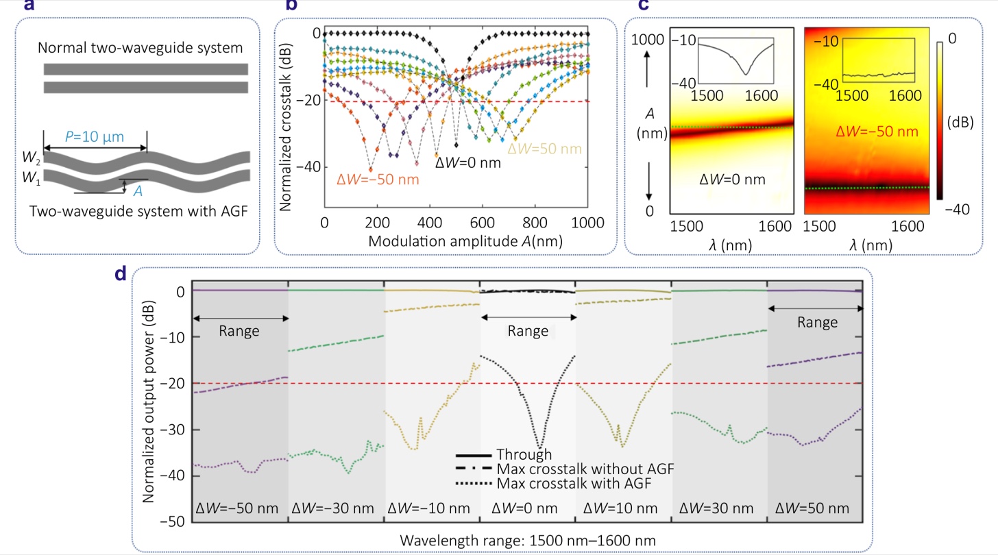
原文 Fig. 2 图注:Broadband crosstalk suppression enabled by combining AGF and propagation-constant mismatch. (a) Schematics of TWSes without AGF (top) and with AGF introduced via sinusoidal trajectory modulation (bottom). (b) Simulated normalized crosstalk at 1550 nm as a function of modulation amplitude $A$ for TWSes with different waveguide width differences $\Delta W$ (from −50 to 50 nm). (c) Simulated normalized crosstalk as functions of modulation amplitude and wavelength for $\Delta W=0$ nm (left) and $\Delta W=-50$ nm (right). Insets show the crosstalk spectra at the optimal modulation amplitudes, $A=500$ nm (left) and $A=160$ nm (right), marked by green dotted lines. (d) Simulated normalized output spectra of TWSes with different width differences, comparing devices without AGF (dash-dotted line) and with AGF (dash line). In (b, c), the modulation amplitude corresponds to the condition yielding minimum crosstalk, the width difference is defined as $\Delta W = W_2 - W_1$, and the TWS length is 100 μm.
Figure 2(a) illustrates two TWS configurations with identical waveguide thickness (220 nm) and silicon dioxide cladding. In the reference case, both waveguides have equal widths ($W_1 = W_2 = 500$ nm), while in the AGF assisted case, a sinusoidal trajectory with fixed period $P = 10$ μm is applied (lower panel). We fix the width of waveguide 1 ($W_1 = 500$ nm) and vary the width of waveguide 2, $W_2$, such that the width deviation $\Delta W = W_2 - W_1$ spans from −50 to +50 nm, while simultaneously sweeping the modulation amplitude $A$ from 0 to 1000 nm. Light is launched into waveguide 1, and the output power from waveguide 2 is recorded as the crosstalk. Figure 2(b) shows the crosstalk at 1550 nm as a function of $A$ for different $\Delta W$. For each $\Delta W$, a distinct modulation amplitude produces a CDT condition with crosstalk as low as −35 dB. For $\Delta W > 0$, larger width detuning requires larger modulation amplitude, whereas the opposite trend is observed for $\Delta W < 0$. Importantly, even away from the CDT condition, width-detuned TWSes consistently exhibit lower crosstalk than the uniform case. As $\lvert\Delta W\rvert$ increases, the crosstalk curve becomes progressively flatter near CDT, indicating enhanced tolerance to fabrication-induced variations in $A$ for achieving crosstalk lower than −20 dB (see Supplementary Section 2 for details).
The broadband response is further illustrated in Fig. 2(c), which plots crosstalk as a function of wavelength and modulation amplitude for $\Delta W = 0$ nm and $\Delta W = -50$ nm. To exclude sampling artifacts, we monitor the electric field in waveguide 2 ($W_2$) after each modulation period and record the maximum power (see Supplementary Section 3 for details). For the uniform TWS (left panel), low crosstalk (<−20 dB) occurs only near a narrow amplitude range around $A \approx 500$ nm (green dotted line in the left panel of Fig. 2(c)), and the optimal suppression wavelength shifts with $A$. In contrast, for $\Delta W = -50$ nm, a nearly wavelength-independent suppression band emerges at $A = 160$ nm (green dotted line in the right panel of Fig. 2(c)), yielding robust crosstalk suppression from 1500 to 1600 nm.
We summarize the simulated transmission and crosstalk for TWSes with $\Delta W = 0$, 10 nm, 30 nm, 50 nm in Fig. 2(d). Compared with the normal TWS ($\Delta W = 0$) without AGF (dash-dotted lines), AGF engineering reduces crosstalk by approximately 20 dB for a given waveguide width mismatch. When $\lvert\Delta W\rvert \ge 30$ nm, crosstalk remains below −25 dB across the entire band. However, for $\Delta W > 0$, performance degrades due to the larger modulation amplitude required, which introduces bending-induced deviations from ideal AGF behavior. Consequently, configurations with $\Delta W < 0$ and smaller $\lvert\Delta W\rvert$ are preferred, offering superior broadband isolation with reduced bending loss (see Supplementary Section 4 for details).
In straight waveguide arrays, propagation constant mismatch is constrained by single mode conditions and half-wavelength pitch requirements. As indicated by the red arrow in Fig. 3(a), strong coupling to second-nearest neighbors becomes (waveguide 2 to the other waveguide 2) significant at small pitches, necessitating deliberate subarray design. Following the $\Delta W < 0$ criterion, we construct a subarray with monotonically decreasing waveguide widths (Fig. 3(d)). With a fixed pitch of 750 nm and to limit propagation loss in narrow waveguides, widths are restricted to 400–550 nm. Four selected widths (stars in Fig. 3(b)) form a four-waveguide subarray (FWS) with mutually compatible propagation-constant mismatches, enabling uniform modulation.
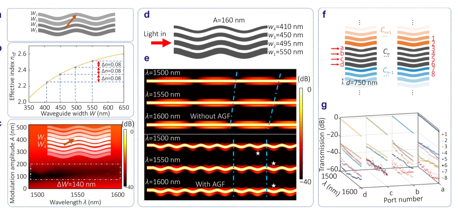
原文 Fig. 3 图注:Subarray-assisted design for half-wavelength–pitched dense waveguide arrays. (a) Schematic of a subarray consisting of two AGF assisted TWSes. (b) Effective index of an isolated waveguide as a function of waveguide width. Blue stars mark the selected widths used in the FWS. (c) Simulated crosstalk spectra between the upper and lower FWSes (indicated by the red arrow) as a function of modulation amplitude (0–500 nm). The white dash-dotted rectangle highlights the region of strong crosstalk suppression. (d, e) Schematic (d) and normalized field evolution (e) of an FWS without (top) and with AGF (bottom, $A=160$ nm). Blue dash-dotted lines indicate the cycle lengths at which minimum crosstalk occurs, while white stars mark half-cycle positions corresponding to maximum crosstalk. (f) Schematic of the proposed non-uniform dense waveguide array with a 750 nm pitch, constructed by periodic arrangement of FWS subarrays. (g) Simulated normalized output power $T_{nm}$ ($n=a, b, c, d$; $m=1-8$) measured at different output waveguides.
For the FWS-formed array in Fig. 3(c), a larger width contrast between adjacent FWSes ($\Delta W_{41} = W_4 - W_1 = 140$ nm) further suppresses inter-subarray coupling. Crosstalk remains below −20 dB for all modulation amplitudes and reaches −40 dB near $A \approx 160$ nm. Field evolution simulations (Fig. 3(e)) reveal that, by injecting light into waveguide 2 (Fig. 3(d)), without AGF, the FWS exhibits strong wavelength-dependent dispersion as indicated by the tilted blue dash-dotted lines in the upper panel of Fig. 3(e) (see Supplementary Section 5 for details), whereas AGF engineering synchronizes coupling cycles across wavelengths as shown by vertical blue dash-dotted lines in the lower panel of Fig. 3(e), enabling broadband suppression. At half-period propagation (white stars), nearest-neighbor crosstalk remains below −20 dB.
A dense waveguide array with half-wavelength pitch is realized by periodically repeating the FWS (Fig. 3(f)). We evaluate the performance of this array by sequentially launching light into each of the four waveguides (ports a–d) of a representative subarray $C_n$, and monitoring the output power at eight waveguides (ports 1–8). To accurately quantify inter-waveguide coupling, we record the electric field distribution after each modulation period and define the crosstalk as the maximum coupled power observed over the propagation length. Using the 3D FDTD solution, we numerically simulate the performance for a propagation distance of 500 μm, with the results summarized in Fig. 3(g). Across the entire wavelength band, the crosstalk remains below −30 dB for both nearest neighbors (NNs) and second-nearest neighbors (SNNs), while coupling to more distant waveguides (third and fourth neighbors) is negligible. Importantly, the transmission of the excited waveguide remains close to 0 dB, indicating minimal bending-induced excess loss and confirming the high efficiency of the proposed dense waveguide architecture.
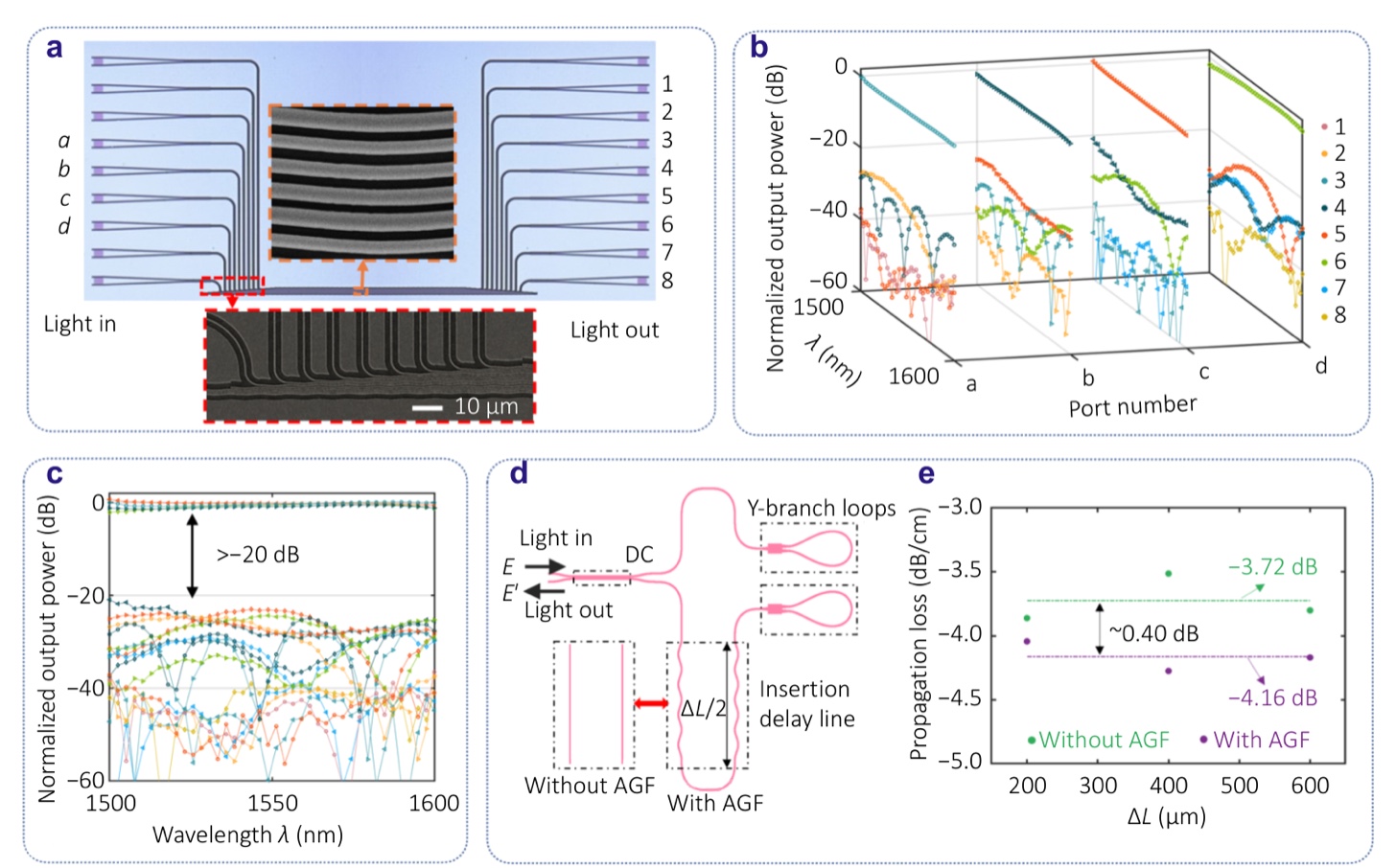
原文 Fig. 4 图注:Experimental characterization of the dense waveguide array and bending-induced loss. (a) Optical microscope image and scanning electron micrograph (SEM) of the fabricated dense waveguide array. (b) Three-dimensional and (c) 2D views of the measured normalized output spectra for different input ports (a–d), showing transmission and crosstalk contributions from NNs and SNNs. (d) Schematic of the Michelson interferometer (MI) used to characterize bending-induced propagation loss. (e) Extracted propagation loss from the normalized transmission spectra (Fig. S10) for waveguides without AGF (green) and with AGF (purple).
Devices were fabricated following established procedures (see methods)34,35, yielding an 8-channel array with propagation length exceeding 500 μm (Fig. 4(a)). To minimize interface-induced coupling, adjacent channels are longitudinally offset by one modulation period, and additional dummy waveguides are included to emulate a large-scale array. Figure 4(b) illustrates the normalized output spectra of eight waveguides (port 1 to port 8) when light is launched into the four input channels (port a to port d). The through-channel insertion loss is below 1 dB with a power variation ($\sigma$) of less than 1.5 dB over the entire 100 nm bandwidth (see Supplementary Section 6), while the measured crosstalk remains below −20 dB from 1500 to 1600 nm for both nearest and second-nearest neighbors (Fig. 4(c)). Residual discrepancies between experiment and simulation are attributed to sidewall-roughness-induced incoherent scattering and fabrication-induced deviations in waveguide width and modulation amplitude.
It is well known that waveguide bending can introduce additional propagation loss due to reduced optical confinement29,36. Although such effects are carefully mitigated during the design stage, experimental quantification of bending-induced loss is essential. To this end, we design a modified Mach–Zehnder interferometer (MZI) incorporating a closed Y-branch loop in each arm, as shown in Fig. 4(d). This configuration allows us to extract the loss of the inserted modulated section (highlighted in gray) independently of power-splitter imbalance. The propagation loss of each delay line is determined from the extinction ratio (ER) of the interference fringes, as detailed in Supplementary Section 7. Figure 4(f) compares the measured loss of straight waveguides with and without AGFs for varying delay line lengths. The averaged propagation loss of standard straight waveguides is 3.72 dB/cm, whereas AGF-modulated waveguides exhibit a slightly higher loss of 4.16 dB/cm. This indicates that the additional loss introduced by trajectory modulation is approximately 0.4 dB/cm. We attribute this excess loss primarily to fabrication-induced sidewall roughness and process nonuniformities (see Supplementary Section 8). Further optimization of fabrication techniques is expected to reduce this loss and further enhance array performance.
2.2 Dispersionless power splitter
Conventional optical power splitters inherently exhibit strong wavelength dependence, which fundamentally limits their ability to provide stable broadband intensity shaping. To overcome this constraint, we simultaneously engineer the waveguide geometry and the AGF modulation amplitude to compensate for normal phase dispersion, thereby enabling broadband and arbitrarily configurable optical power splitting ratios.
As described in Eqs. (1) and (2), both $\kappa_{\rm eq}$ and $J_0(a)$ are wavelength-dependent. Taking the derivative of $\kappa_{\rm eq}$ with respect to $\lambda$ yields the AGF-induced effective dispersion $\Upsilon_{\rm eq}$ (see details in Supplementary Section 9):
\[\Upsilon_{\rm eq} = \frac{\partial \kappa_{\rm eq}(\lambda)}{\partial \lambda} = J_0\big(a(\lambda)\big)\big(\Upsilon_0 + \Upsilon_{\rm AGF}\big), \qquad (3)\] \[\Upsilon_{\rm AGF} = \kappa(\lambda)\frac{a}{\lambda}\frac{J_1(a(\lambda))}{J_0(a(\lambda))}\left(1 - \frac{\partial n_{\rm e}(\lambda)/\partial \lambda}{n_{\rm e}(\lambda)/\lambda}\right), \qquad (4)\]where $\Upsilon_0$ represents the intrinsic coupling dispersion of a conventional directional coupler (DC). As illustrated in Fig. 5(a), within the shaded region, $J_0(a(\lambda))$ and $J_1(a(\lambda))$ possess opposite signs, allowing the ratio $J_1(a(\lambda))/J_0(a(\lambda))$ to vary continuously from $-\infty$ to 0. Given that $\Upsilon_0 > 0$ and $\partial n_{\rm e}(\lambda)/\partial\lambda \big/ \big(n_{\rm e}(\lambda)/\lambda\big) < 0$, an appropriate choice of modulation amplitude enables the condition $\lvert\Upsilon_{\rm AGF}\rvert = \lvert\Upsilon_0\rvert$, resulting in a vanishing effective dispersion $\Upsilon_{\rm eq} = 0$. This dispersion cancellation forms the physical basis for broadband, wavelength-insensitive power splitting.
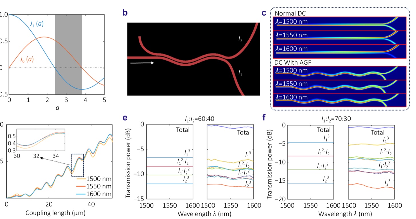
原文 Fig. 5 图注:Dispersionless power splitters with arbitrary splitting ratios. (a) 0th and 1st order Bessel functions, $J_0(a)$ and $J_1(a)$, as functions of the modulation parameter $a$. (b) Schematic of the AGF-engineered dispersionless power splitter. (c) Simulated electric field evolution for a conventional directional coupler (top) and AGF-based directional coupler (bottom) at different wavelengths, illustrating wavelength-insensitive coupling in the AGF design. (d) Cross port output power ($I_2$) as a function of coupling length. (e, f) Comparison between simulated and measured transmission power for power-splitting ratios of $I_1:I_2 = 60{:}40$ (e) and $I_1:I_2 = 70{:}30$ (f). Curves from top to the bottom correspond to the total power, $I_1^{3}$, $I_1^{2}\cdot I_2$, $I_1\cdot I_2^{2}$, $I_2^{3}$.
Figure 5(b) depicts the AGF-assisted directional coupler consists of identical silicon waveguides with widths of 500 nm, a thickness of 220 nm, a gap of 200 nm, and a modulation period of 10 μm. By fixing the modulation amplitude at 700 nm and appropriately selecting the coupling length $L$, near-dispersionless coupling ratios can be achieved. Figure 5(c) compares the simulated electric field evolution of a conventional DC (upper panel) and an AGF-engineered coupler (lower panel) for a 50:50 splitting ratio at three representative wavelengths. In contrast to the strong wavelength dependence observed in the conventional device, the AGF-based coupler maintains an identical field evolution profile across the entire 1500–1600 nm range. Figure 5(d) further illustrates the coupling power as a function of coupling length, confirming broadband coupling behavior. Building upon this approach, we design and fabricate two broadband power splitters with target power ratios of 60:40 and 70:30, corresponding to coupling lengths of $L_{0.4} = 27.9$ μm and $L_{0.3} = 23.1$ μm, respectively. Each splitter is implemented as a three-stage cascaded array. Figure 5(e, f) present the simulated and measured transmission spectra of the fabricated devices. Across the wavelength range from 1500 to 1600 nm, both splitters exhibit minimal wavelength dependence, with power ratios closely matching theoretical predictions. The maximum power variation ($\sigma$) across the entire bandwidth is less than 0.77 dB, indicating the effectiveness of AGF-enabled dispersion compensation (see Supplementary Section 8).
2.3 On-chip optical phased array with wide FoV and high SLL
One important application of this dispersionless, half-wavelength pitched dense waveguide array is the realization of an on-chip OPA with a wide FoV. A half-wavelength pitch theoretically ensures the presence of only a single main lobe within a 180° FoV17. However, for a uniform channel intensity distribution, the maximum far-field SLL is fundamentally limited to −13.46 dB, which is insufficient for applications requiring high sidelobe suppression. To further demonstrate the effectiveness of crosstalk suppression and to reduce SLLs, we employ a beamforming strategy based on a Gaussian channel intensity distribution37,38. Unlike a uniform phased array, the optical intensity in each channel follows a Gaussian profile, described by the normalized amplitude:
\[E(n) = e^{\,-4\ast(n - N/2)^2 \big/ \xi N^2}, \qquad (5)\]where $\xi$ is the distribution factor. Figure 6(a, b) show the channel intensity distributions for different values of $\xi$ and the corresponding far-field patterns at $\theta = 0°$. For sufficiently large $\xi$ (e.g., $\xi = 100$), the distribution approaches uniformity. As $\xi$ decreases, the SLL is significantly reduced, reaching values below −40 dB at $\xi = 0.75$. This improvement, however, comes at the expense of a broader main lobe due to reduced total far-field contribution39. A balance must therefore be struck between sidelobe suppression and beamwidth. In this work, we select $\xi = 2$, which yields a theoretical SLL of −23 dB with less than 10% beamwidth broadening. In practical two-dimensional OPAs, beam steering is achieved through a combination of phase tuning and wavelength sweeping. Maintaining low sidelobe levels during wavelength tuning requires a broadband Gaussian intensity distribution.
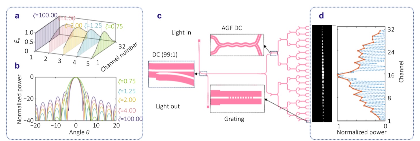
原文 Fig. 6 图注:Channel intensity engineering for sidelobe suppression. (a) Designed intensity distribution of the 32-channel array for different Gaussian distribution factors $\xi$. (b) Corresponding far-field radiation patterns for a half-wavelength-pitched array. (c) Schematic of the cascaded power splitter network implementing the 32-channel array for $\xi = 2$. (d) Experimentally measured optical power distribution across the 32 channels.
Using the dispersionless power-splitting approach enabled by AGF engineering, we implement a 32-channel array suitable for broadband OPA operation (Fig. 6(c)). Based on the target Gaussian intensity distribution ($\xi = 2$, Fig. 6(a)), the required coupling ratios and corresponding coupling lengths are determined, as summarized in Supplementary Table S3. The experimentally measured scattering intensities from each grating antenna, obtained using a near-infrared microscopy setup, are shown in Fig. 6(d) at a wavelength of 1550 nm. Despite minor deviations arising from fabrication tolerances, the measured channel intensity distribution closely agrees with the designed Gaussian profile, thereby validating the effectiveness of the proposed broadband, near-dispersionless power-splitting strategy.
Finally, we implement a 2D OPA by integrating the half-wavelength-pitched, dispersionless dense waveguide array with a cascaded dispersionless optical power splitter, thermo-optic phase shifters, and grating antennas, as illustrated in Fig. 7(a). The far-field radiation patterns are captured using a rotated CCD camera positioned above the chip. Assisted by a calibration port, a particle swarm optimization (PSO) algorithm is employed to rapidly compensate phase errors across channels, enabling precise beam focusing at $\theta = 0°$. By selecting appropriate input optical power to avoid CCD saturation, we measure the normalized far-field intensity as a function of wavelength along the $\varphi$ direction (Fig. 7(b)). As the wavelength is tuned from 1500 to 1600 nm, the beam center shifts from +16.5° to +2°, corresponding to a tuning efficiency of 0.14°/nm. The measured beamwidths are $\Delta\theta = 4.1°$ and $\Delta\varphi = 1.2°$, with corresponding sidelobe levels (SLLs) of −18.2 dB and −17.9 dB (Fig. 7(c)), significantly lower than the −13.46 dB characteristic of uniform phased arrays. As shown in Fig. 7(d), the SLL gradually increases as the beam is steered toward larger angles, reaching −15.1 dB at −30° and −10.3 dB at +60° (see detailed analysis in Supplementary Section 10). Nevertheless, as summarized in Fig. 7(e), the demonstrated device supports 2D beam steering over a FoV of 120° × 14.5°.
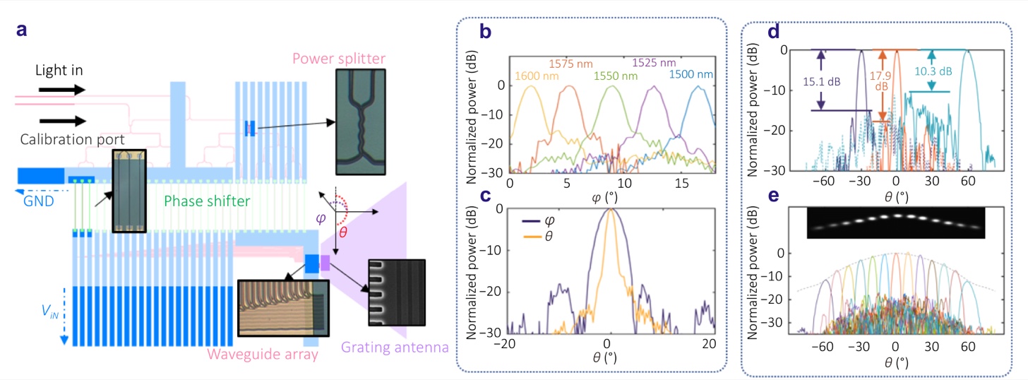
原文 Fig. 7 图注:2D OPA based on the dense waveguide array and power splitters. (a) Schematic of the integrated 2D OPA comprising the dense waveguide array, cascaded power splitters, thermo-optic phase shifters, and grating antennas. (b) Measured far-field interference patterns at five representative wavelengths with the main beam steered to $\theta = 0°$. (c) Measured far-field beam profiles at 1550 nm along the $\varphi$ and $\theta$ directions. (d) Beam steering at 1550 nm for steering angles of −30°, 0°, +60°. Solid lines highlight the main lobes for clarity. (e) Measured normalized far-field intensity along the $\theta$ direction. Upper inset: composite far-field image showing continuous beam scanning from −60° to +60°.
Owing to the strong broadband crosstalk suppression enabled by AGF engineering and optimized channel apodization, the far-field patterns exhibit consistently low sidelobe levels across this wide angular range.
3 Conclusion
Precise control of optical coupling is a fundamental requirement for high-density photonic integrated circuits, yet evanescent coupling between closely spaced waveguides intrinsically limits integration density and operational bandwidth. In particular, achieving broadband, low-crosstalk operation in half-wavelength-pitch waveguide arrays remains a longstanding challenge due to strong wavelength-dependent coupling. Here, we present a unified AGF–based framework that enables broadband manipulation of optical coupling in densely packed silicon waveguide arrays. By combining propagation-constant mismatches introduced through deliberate waveguide-width variations with carefully engineered sinusoidal trajectory modulations, we achieve wavelength-insensitive suppression of coupling across ultra-dense waveguide arrays with a 750 nm pitch. Experimental measurements demonstrate crosstalk below −20 dB over a broad wavelength range from 1500 to 1600 nm, with negligible additional propagation loss. Beyond coupling suppression, we further exploit AGF-induced dispersion engineering to realize dispersionless directional couplers with arbitrary, wavelength-independent power-splitting ratios. Cascading these dispersionless couplers enables the synthesis of broadband Gaussian intensity distributions across large channel counts.
Integrating the dispersionless dense waveguide array and broadband power-splitting network, we demonstrate a 2D OPA featuring a wide FoV of 120° × 14.5° and SLL below −17 dB. Our results establish AGF engineering as a powerful and scalable strategy for broadband coupling control, enabling substantial reductions in waveguide spacing while preserving performance. This approach provides a versatile platform for next-generation high-density photonic systems, including optical phased arrays, compact delay lines, and space-division multiplexed photonic interconnects.
4 Methods
4.1 Fabrication
The dense waveguide array was fabricated on a 15 × 15 mm² chip cleaved from a standard silicon-on-insulator (SOI) wafer comprising a 220 nm thick silicon membrane and a 2 μm thick buried oxide layer. Prior to lithography, the sample was sequentially ultrasonically cleaned in deionized water, acetone, and isopropanol, followed by dehydration in an O₂ plasma for 3 minutes. A high-resolution positive electron beam resist (ZEP520A, ZEONREX) with a thickness of approximately 300 nm was spin-coated at 6000 rpm for 60 s (acceleration: 2000 rpm s⁻¹) and prebaked at 180 °C for 2 minutes. Electron-beam lithography (EBL) was performed using an Elionix ELS-F125G8 system operated at an acceleration voltage of 125 keV and a beam current of 1 nA. The patterns were defined with shot pitch, feed pitch, and scan pitch values of 1 nm, 5 nm, and 5 nm, respectively. Following exposure at a dose of 180 μC cm⁻², the resist was developed in ZED-N50 (n-amyl acetate) for 60 s and rinsed in ZMD-B (methyl isobutyl ketone), followed by a soft bake at 120 °C to enhance etch resistance. Fully etched silicon waveguides were subsequently formed by inductively coupled plasma reactive ion etching (ICP-RIE; PlasmaPro 100 Cobra 180) using HBr/Cl₂ chemistry at an RF power of 50 W and an ICP power of 800 W for 55 s. A 1 μm-thick silicon dioxide cladding layer was then deposited by plasma-enhanced chemical vapor deposition (PECVD). Metal heaters and electrical interconnects were defined using maskless lithography (MLA150). A 100 nm-thick titanium adhesion layer followed by a 600 nm-thick aluminum layer was sequentially deposited and patterned via a lift-off process. Finally, the contact pads were wire-bonded to a printed circuit board (PCB) for electrical interfacing.
4.2 Measurement
Device characterization was performed using a supercontinuum light source (SuperK Fianium) covering the wavelength range from 1500 to 1600 nm. Light was coupled into the dense waveguide array via grating couplers, and the output signal was collected from the chip and analyzed using an optical spectrum analyzer (Yokogawa AQ6370E) to obtain transmission spectra.
For OPA measurements, a tunable continuous-wave laser (Keysight 81607A), in conjunction with a fiber optic attenuator, was employed as the input source. The far-field interference patterns radiated by the shallow-etched grating antennas were recorded using a near-infrared camera (Hamamatsu C12741-03).
Thermo-optic phase shifters were driven by a digital-to-analog converter (National Instruments PXIe-6739) and required approximately 39 mW of electrical power to achieve a full 2π phase shift. To compensate for phase errors arising from fabrication-induced path-length variations and device nonuniformities, a particle swarm optimization (PSO) algorithm was implemented for rapid phase calibration across all channels.
Acknowledgements
The authors thank the ShanghaiTech Material Device Lab (SMDL), Core Facility Platform of Electronics of ShanghaiTech University, and Max-Optics Technology Co., Ltd, for their technical support. The research is sponsored by Natural Science Foundation of Shanghai (21ZR1443100); Key Research and Development Program of Ningxia Hui Autonomous Region (2025BEG01003).
Author contributions
T. L. and Y. Z. conceived the idea; T. L. proposed the design and performed the numerical simulations; T. L. and Y. S. fabricated the samples; T. L. and H. Z. performed the optical measurement; T. L. and Y. Z. analyzed the results, T. L. wrote the manuscript with the input from all authors. X. X. and T. X. provided advisory support in preparing the manuscript. Y. Z. supervised the project, provided funding support, and polished the manuscript.
Competing interests
The authors declare that they have no competing interests.
Data availability
All data needed to evaluate the conclusions in the paper are present in the paper and/or the Supplementary Materials.
Supplementary information
Supplementary information for this paper is available at https://doi.org/10.29026/oea.2026.260026.
References
- Mukherjee S, Mogilevtsev D, Slepyan GY et al. Dissipatively coupled waveguide networks for coherent diffusive photonics. Nat Commun 8, 1909 (2017).
- Vlk M, Datta A, Alberti S et al. Extraordinary evanescent field confinement waveguide sensor for mid-infrared trace gas spectroscopy. Light Sci Appl 10, 26 (2021).
- Yao CH, Zhang WL, Bao P et al. Chip-scale sensor for spectroscopic metrology. Nat Commun 15, 10305 (2024).
- Mao D, Wang Y, El-Fiky E et al. Adiabatic coupler with design-intended splitting ratio. J Lightwave Technol 37, 6147–6155 (2019).
- Zhu R, Qian CJ, Xiao S et al. Full polarization control of photons with evanescent wave coupling in the ultra subwavelength gap of photonic molecules. Light Sci Appl 14, 114 (2025).
- Song WG, You OB, Sun JC et al. Fast topological pumps via quantum metric engineering on photonic chips. Sci Adv 10, eadn5028 (2024).
- Vicencio RA, Román-Cortés D, Rubio-Saldías M et al. Nonsymmetric evanescent coupling in photonics. Phys Rev A 111, 043510 (2025).
- Yang Y, Chapman RJ, Haylock B et al. Programmable high-dimensional Hamiltonian in a photonic waveguide array. Nat Commun 15, 50 (2024).
- Chang C, Sun YH, Li T et al. Coupling-controlled photonic topological ring array. ACS Photonics 11, 5260–5266 (2024).
- Jahani S, Kim S, Atkinson J et al. Controlling evanescent waves using silicon photonic all-dielectric metamaterials for dense integration. Nat Commun 9, 1893 (2018).
- Huang HZ, Chen HX, Liu HG et al. High-intensity spatial-mode steerable frequency up-converter toward on-chip integration. Opto-Electron Sci 3, 230036 (2024).
- Hong SH, Zhang L, Wu JC et al. Multimode-enabled silicon photonic delay lines: break the delay-density limit. Light Sci Appl 14, 145 (2025).
- Yu L, Wang PF, Ma PF et al. Two-dimensional beam scanning of passive optical phased array based on silicon nitride delay line. J Lightwave Technol 41, 2756–2764 (2023).
- Poulton CV, Byrd MJ, Russo P et al. Coherent LiDAR with an 8,192-element optical phased array and driving laser. IEEE J Sel Top Quantum Electron 28, 6100508 (2022).
- Sun J, Timurdogan E, Yaacobi A et al. Large-scale nanophotonic phased array. Nature 493, 195–199 (2013).
- Yue GC, Li Y. Integrated lithium niobate optical phased array for two-dimensional beam steering. Opt Lett 48, 3633–3636 (2023).
- Liu Y, Hu H. Silicon optical phased array with a 180-degree field of view for 2D optical beam steering. Optica 9, 903–907 (2022).
- Qi YF, Yue GC, Hao T et al. Strong-confinement low-index-rib-loaded waveguide structure for etchless thin-film integrated photonics. Opto-Electron Adv 8, 250056 (2025).
- Song WG, Li T, Wu SJ et al. Dispersionless coupling among optical waveguides by artificial gauge field. Phys Rev Lett 129, 053901 (2022).
- Zhou PJ, Zhang H, Liu YH et al. All-zero tunneling rates in an ultra-dense waveguide array. Laser Photonics Rev 19, e00207 (2025).
- Lin Q, Fan SH. Light guiding by effective gauge field for photons. Phys Rev X 4, 031031 (2014).
- Zhou PJ, Li T, Lin YC et al. Artificial gauge field enabled low-crosstalk, broadband, half-wavelength pitched waveguide arrays. Laser Photonics Rev 17, 2200944 (2023).
- Shekhar S, Bogaerts W, Chrostowski L et al. Roadmapping the next generation of silicon photonics. Nat Commun 15, 751 (2024).
- Li T, Zhang H, Zhou PJ et al. Morphology engineering enabled mid-infrared ultra-dense waveguide array with low crosstalk. Laser Photonics Rev 18, 2400297 (2024).
- Qin YY, Gu XW, Ye HY et al. Broadband lithium niobate integrated microwave photonic beamforming chip. Laser Photonics Rev 19, e00219 (2025).
- Xu XB, Guo X, Chen W et al. Flat-top optical filter via the adiabatic evolution of light in an asymmetric coupler. Phys Rev A 100, 023809 (2019).
- Van Campenhout J, Green WM, Assefa S et al. Low-power, 2×2 silicon electro-optic switch with 110-nm bandwidth for broadband reconfigurable optical networks. Opt Express 17, 24020–24029 (2009).
- Mia MB, Ahmed SZ, Ahmed I et al. Exceptional coupling in photonic anisotropic metamaterials for extremely low waveguide crosstalk. Optica 7, 881–887 (2020).
- Zafar H, Paredes B, Villegas J et al. O-band TE- and TM-mode densely packed adiabatically bent waveguide arrays on the silicon-on-insulator platform. Opt Express 31, 21389–21398 (2023).
- Song WW, Gatdula R, Abbaslou S et al. High-density waveguide superlattices with low crosstalk. Nat Commun 6, 7027 (2015).
- Yariv A. Coupled-mode theory for guided-wave optics. IEEE J Quantum Electron 9, 919–933 (1973).
- Longhi S. Coherent destruction of tunneling in waveguide directional couplers. Phys Rev A 71, 065801 (2005).
- Grossmann F, Dittrich T, Jung P et al. Coherent destruction of tunneling. Phys Rev Lett 67, 516–519 (1991).
- Liu YH, Xia LP, Li T et al. High-efficiency mid-infrared on-chip silicon grating couplers for perfectly vertical coupling. Opt Lett 48, 239–242 (2023).
- He WC, Sun YH, Zhou PJ et al. Subwavelength structure engineered passband filter for the 2-µm wave band. Opt Lett 48, 827–830 (2023).
- Gatdula R, Abbaslou S, Lu M et al. Guiding light in bent waveguide superlattices with low crosstalk. Optica 6, 585–591 (2019).
- Chen C, Kong DGG, Tao YF et al. Half-wavelength-pitch silicon optical phased array with a 180° field of view, high sidelobe suppression ratio, and complex-pattern beamforming. Optica 11, 1575–1582 (2024).
- Zhao S, Lian DX, Li WL et al. Low sidelobe silicon optical phased array with Chebyshev amplitude distribution. Nanophotonics 13, 263–269 (2024).
- Sharma A, Straguzzi JN, Xue TY et al. Optimization of a programmable λ/2-pitch optical phased array. Nanophotonics 13, 2241–2249 (2024).
第二部分:中文结构化解读
以下为独立撰写的中文解读,非原文翻译。文中带核算、质疑与边界判断的内容属解读者观点,不代表原作者立场。原文所有给出公式与几何参数的地方我都重新算过,结果与差异在第八节逐条列出。
一、一句话定位
这是一篇把「近邻波导互相串光」这件硅光的根本性麻烦,从「只能绕开」变成「可以主动设计掉」的论文。
它做了两件事,共用同一套物理机制:
- 耦合抑制:在 SOI 上做出中心距 750 nm 的密集波导阵列(1550 nm 处半波长约 775 nm,750 nm 已低于半波长),1500–1600 nm 全带实测串扰低于 −20 dB,且几乎没有额外损耗。
- 耦合调控:用同一机制把耦合的波长依赖(色散)主动抵消,做出 60:40 与 70:30 的「无色散」分光器,再用它级联出 32 通道高斯加权阵列,集成出视场 120° × 14.5°、旁瓣低于 −17 dB 的二维光学相控阵(OPA)。
两件事看似不同,其实是同一个旋钮的两面:人造规范场(AGF)既能让你把耦合调到零,也能让你把耦合的导数调到零。
二、问题的物理内核:耦合的两个「恶魔」
理解全文要先接受一个前提:在集成光子学里,波导之间「不该耦合的耦合」是密度与带宽的双重枷锁。它有两个互相独立的坏性质:
| 性质 | 数学形式 | 工程后果 |
|---|---|---|
| 耦合强度随间距指数上升 | $\kappa \propto e^{-d/d_0}$ | 想把间距缩到亚微米,耦合就爆炸;OPA 想要的半波长间距恰好落在爆炸区 |
| 耦合强度随波长显著变化 | $\kappa(\lambda)$ 由材料色散 + 几何色散共同决定 | 想要宽带工作的器件(波分解复用器、波长扫描 OPA)没有一个稳定的工作点 |
第一条决定了「最小允许间距」,第二条决定了「工作带宽」。传统做法(弯曲波导、超晶格、超材料)都在对付第一条,代价是第二条更严重——这正是作者在 Introduction 里划的靶心:已有的 AGF 工作能在某个特定波长把耦合做到近乎完全抑制,但那个「特定」太特定。
三、人造规范场(AGF)与相干隧穿破坏(CDT)
这里有一处必须先讲清的物理图像,否则后文全是公式。
波导如果不走直线,而是沿传播方向做正弦轨迹摆动,那么在弯曲坐标系里看,光感受到的是一个等效的周期势——这就是「人工规范场」。对两根波导的耦合而言,摆动的效果不是让耦合变大或变小,而是让耦合系数被一个相位因子反复调制,其周期平均正好是零阶贝塞尔函数:
\[\kappa_{\rm eq} = \kappa_{1,2}\,J_0(a), \qquad a = \frac{4\pi^2 n A d}{P\lambda_0}\]其中 $A$ 是轨迹摆幅、$P$ 是摆动周期、$d$ 是波导中心距、$n$ 是折射率、$\lambda_0$ 是工作波长。
这个式子的物理含义很干净:耦合强度变成了一个可以通过几何参数 $A$ 连续调节的量,而 $J_0(a)$ 会周期性过零。第一次过零在 $a = 2.405$——此时等效耦合为零,光完全留在原波导,这就是相干隧穿破坏(CDT)。零阶贝塞尔函数在这里扮演的角色,本质上是「周期调制的相干平均」。
但魔鬼藏在 $a$ 的定义式里:$a \propto 1/\lambda_0$。也就是说,你为 1550 nm 调好的 $A$,到了 1600 nm 就不对了。$J_0(a)$ 的零点在波长轴上是一条极窄的线——如图 1(b) 那个绿色虚线框所示,只有很窄的一段波长还能算「被抑制」。这正是原文要打的第一个洞。
四、本文的关键一步:把「失配」从敌人变成朋友
作者的动作非常直接:既然单一旋钮(轨迹摆幅 $A$)不够,就再加一个旋钮(波导宽度)。
宽度不同 → 两根波导的传播常数不同 → 得到 $\Delta = (\beta_2 - \beta_1)/2$ 这个对角失配角。Eq. (1) 的 2×2 耦合模方程因此从「简并耦合」变成「失谐耦合」:
\[i\frac{\partial}{\partial z}\begin{bmatrix} c_1 \\ c_2 \end{bmatrix} = \begin{bmatrix} \rho_1 + \Delta & \kappa_1 X(a) \\ \kappa_2 X(a) & \rho_2 - \Delta \end{bmatrix} \begin{bmatrix} c_1 \\ c_2 \end{bmatrix}\]关键在于这两个旋钮不是简单的叠加,而是有耦合的:
- Fig. 2(b) 显示,同一个 $A$ 下,给不同的 $\Delta W$,最低串扰点会移动到不同的 $A$;$\Delta W > 0$ 要更大的摆幅,$\Delta W < 0$ 反而要更小的摆幅。
- Fig. 2(c) 是全文最有信息量的一张图:把串扰画成「摆幅 × 波长」的二维热图。均匀波导(左,$\Delta W = 0$)时,低串扰只在一条斜线附近的窄摆幅带里出现——摆幅与波长相互绑架;而 $\Delta W = -50$ nm(右)时,低串扰区变成一条水平带,横跨整个 1500–1600 nm。
- 那句「$\lvert\Delta W\rvert$ 增大时曲线在 CDT 附近变平」值得单独拎出来:它意味着对加工误差的容忍度变好了,这是工程上比「峰值性能」更值钱的性质。
为什么必须是负失配? 原文给的理由是:$\Delta W > 0$ 需要更大的摆幅 $A$,而摆幅越大,弯曲带来的「偏离理想 AGF 行为」的附加损耗越高。所以设计规则是「$\Delta W < 0$ 且 $\lvert\Delta W\rvert$ 尽量小」。这条规则在 Fig. 4 的损耗测试里得到呼应:带 AGF 的波导传播损耗 4.16 dB/cm,比不带 AGF 的 3.72 dB/cm 高 0.44 dB/cm——AGF 不是免费的,摆幅就是它的价码。
五、从两波导到阵列:一个真正的工程化步骤
两波导(TWS)的解漂亮,但阵列面对一个新问题:半波长间距下,隔一个波导的第二近邻耦合(SNN)不可忽略(Fig. 3(a) 那个红箭头)。原文的三级跳值得记录:
1
2
3
4
5
TWS(两根波导,ΔW 可调)
   ↓ 四个宽度单调递减的波导凑成一个子阵列
FWS 四波导子阵列(w1=550 / w2=495 / w3=450 / w4=410 nm)
   ↓ 周期重复,子阵列之间刻意留大宽度对比 ΔW₄₁ = 140 nm
750 nm 间距密集阵列(17 个通道量级 8 通道实测样本)
这里有三个设计决策值得注意:
- 宽度被限制在 400–550 nm:再窄单模条件与损耗都会恶化,这是「传播常数失配」这个自由度被单模条件锁死的直接体现——它不是可以任意取的设计变量,而是有硬边界的。
- 子阵列之间加大宽度对比(140 nm):目的是让相邻子阵列之间「互相不认识」,从而把「阵列」问题拆成「子阵列」问题。这是一种分层解耦的思想。
- 8 通道实测样本 + 纵向错开一个调制周期 + 加 dummy 波导:为了模拟大阵列环境(避免边缘效应)并把「界面耦合」这一项单独消掉。这是实验设计上的细致之处。
仿真结果(3D FDTD,500 μm 传播距离):整个波段内 NN 与 SNN 串扰都低于 −30 dB,三阶以上近邻可忽略,激发波导透过率接近 0 dB。
六、第二块拼图:把色散「抵消」掉
文章后半段从「抑制耦合」转向「调控耦合」,思路是一次漂亮的思路反转:前面把 $J_0(a)$ 的波长依赖当成敌人,现在把它当成可以利用的手段。
\[\Upsilon_{\rm eq} = \frac{\partial \kappa_{\rm eq}}{\partial \lambda} = J_0(a)\big(\Upsilon_0 + \Upsilon_{\rm AGF}\big)\]$\Upsilon_0$ 是传统定向耦合器固有的耦合色散($>0$,即耦合随波长变化)。AGF 通过调制带来一个额外的色散项 $\Upsilon_{\rm AGF}$,而它的表达式里含 $J_1(a)/J_0(a)$ 这个比值。在 $2.405 < a < 3.832$ 这个区间内,$J_0$ 与 $J_1$ 反号,这个比值可以从 $-\infty$ 连续变到 0——于是总能找到一个调制幅度让 $\Upsilon_{\rm AGF} = -\Upsilon_0$,从而 $\Upsilon_{\rm eq} = 0$。
物理图像:传统定向耦合器是「波长变了,耦合就变」;AGF 耦合器是「波长变了,轨迹调制带来的补偿也同步变」,两者相消。
实验落点是 60:40 与 70:30 两个分光器(耦合长度 27.9 μm 与 23.1 μm),三级级联,整带宽内功率起伏小于 0.77 dB。图 5(c) 的对照很直观:传统 DC 在 1500/1550/1600 nm 三个波长下的场演化图明显不同,AGF 版本几乎一模一样。
七、系统级演示:32 通道高斯加权 + 二维 OPA
最后一步是把两块积木拼起来。这里的逻辑链是:
半波长间距阵列 → 无栅瓣的宽视场 ⟶ 但均匀加权时旁瓣上限被锁在 −13.46 dB ⟶ 需要通道幅度加权 ⟶ 加权需要「任意比、且无色散」的分光器 ⟶ 分光器必须无色散,否则波长一扫描,高斯分布就散了,旁瓣就又起来了。
这是全文最漂亮的一处论证:高斯加权之所以必须「宽带的」,不是因为加权本身,而是因为 OPA 靠波长扫描工作。如果分光器有色散,波长一调,32 个通道的幅度比就变了,旁瓣抑制当场失效。
数值上:$\xi$ 越小旁瓣越低,$\xi = 0.75$ 时理论上能压到 −40 dB 以下,但主瓣会明显变宽。作者取 $\xi = 2$(理论 SLL −23 dB,主瓣展宽 < 10%)作为折中。
实测结果:视场 120° × 14.5°,$\theta = 0°$ 附近 SLL −18.2 / −17.9 dB,波长调谐效率 0.14°/nm(100 nm 对应 14°,与 14.5° 视场自洽)。旁瓣随扫描角恶化:−30° 时 −15.1 dB,+60° 时只剩 −10.3 dB,与均匀阵列的 −13.46 dB 已经同一量级甚至更差。这一点原文如实报告了,值得肯定。
八、关键数字清单与我做的复核
8.1 数字总表
| 指标 | 原文数值 | 我的口径说明 |
|---|---|---|
| 通道中心距 | 750 nm | 1550 nm 半波长 = 775 nm,故 750 nm ≈ 0.97 × λ/2,确为亚半波长间距 |
| 串扰抑制 | 仿真 < −30 dB;实测 < −20 dB(NN 与 SNN) | 实测比仿真差约 10 dB,原文归因侧壁粗糙度散射与线宽/摆幅偏差——这是全文最诚实的一段 |
| 工作带宽 | 1500–1600 nm(100 nm) | 即整个 C 波段。O 波段(1260–1360 nm)完全未测 |
| 通带插损 | < 1 dB;功率起伏 $\sigma$ < 1.5 dB | 与 2.2 节的「< 0.77 dB」口径不同(对象不同),见第 11 节 |
| 传播损耗 | 3.72 dB/cm(无 AGF)vs 4.16 dB/cm(有 AGF) | 差 0.44 dB/cm,与原文「约 0.4 dB/cm」一致 ✅ |
| 分光比 | 60:40 / 70:30,$L$ = 27.9 / 23.1 μm | 三级级联,整带 $\sigma$ < 0.77 dB |
| 高斯加权 | $\xi = 2$,理论 SLL −23 dB,主瓣展宽 < 10% | 对比均匀加权 −13.46 dB → 改善约 10 dB |
| 2D OPA | FoV 120° × 14.5°,SLL < −17 dB;调谐 0.14°/nm | 0.14°/nm × 100 nm = 14°,与 14.5° 视场自洽 ✅ |
| 相移功耗 | 39 mW / 2π | 原文给的是单通道数值,未给阵列总功耗 |
8.2 复核一:Bessel 论证的折射率口径(本节最有价值的一条)
Eq. (2) 写了 $a = 4\pi^2 n_{\rm s} A d/(P\lambda_0)$,并在正文里把 $n_{\rm s}$ 明确称为 substrate refractive index(衬底折射率)。但把原文自己给的几何参数代进去,会出现自相矛盾:
算例 A(无色散分光器):波导宽 500 nm、间隙 200 nm → 中心距 $d = 700$ nm;摆动周期 $P = 10$ μm;工作波长 1550 nm;原文取 $A = 700$ nm。
- 若按字面取 $n_{\rm s} = 1.444$(SiO₂):$a = 1.80$,$J_0 = +0.34$,$J_1 = +0.58$ → 同号
- 若取模式有效折射率 $n \approx 2.44$:$a = 3.05$,$J_0 = -0.28$,$J_1 = +0.32$ → 反号 ✅
而原文在推导 Eq. (4) 后明确要求「$J_0(a(\lambda))$ 与 $J_1(a(\lambda))$ 反号」,否则 $\Upsilon_{\rm AGF}$ 不可能与 $\Upsilon_0$ 相消。按字面取衬底折射率,全文的色散抵消机制不成立;取模式有效折射率,一切自洽,且 $a = 3.05$ 恰好落在 $2.405 < a < 3.832$ 这个反号区间内。
算例 B($\Delta W = 0$ 的两波导):原文称最优摆幅 $A \approx 500$ nm(Fig. 2(c) 左)。若取 $d = 750$ nm、$n = 2.44$:$a = 2.33$,$J_0 = +0.04 \approx 0$ ✅ 正好在 CDT 条件 $a = 2.405$ 附近;若取 $n_{\rm s} = 1.444$:$a = 1.38$,$J_0 = +0.58$,离零点很远,无法解释 −35 dB 的抑制。
结论:Eq. (2) 中的 $n$ 实为模式有效折射率,原文标为「substrate refractive index $n_{\rm s}$」属记号命名不清——不是物理错误,但读者若照字面复算会得到与原文矛盾的结论。这类「记号口径」问题在光子学论文里很常见,却最容易让复现者卡住。Fig. 5(a) 里那块灰色阴影区($2.405 < a < 3.832$)正好就是 $J_0$ 与 $J_1$ 反号的区间,也从图上印证了这个判据。
8.3 复核二:孔径与波束宽度
32 通道 × 750 nm 间距 = 24 μm 孔径。均匀照明时衍射极限半高全宽 $\approx 0.886\lambda/D = 0.886 \times 1.55/24 = 3.28°$;高斯加权($\xi = 2$)会再展宽约 10%,即约 3.6°。原文给出的两个轴光束宽度为 4.1° 与 1.2°,与 3.6° 同量级、略宽(约 14%),与「相位标定残差 + 加工误差」的解释一致。量级自洽,没有出现超出衍射极限的可疑数字。
需要如实说明一处对不上:Fig. 7(c) 的两条剖面曲线中,图例标为 $\varphi$ 的那条明显更宽(目测半高全宽在 5° 量级),而正文把 1.2° 归给 $\varphi$。我按图与按文得到的对应关系互相矛盾,无法唯一确定 $\Delta\theta = 4.1°$ 与 $\Delta\varphi = 1.2°$ 分别对应哪条曲线,因此本节不做轴归属判断。这不影响「量级自洽」的结论,但读者对照图与文时可能会困惑。
九、可采信度分层
| 结论 | 等级 | 理由 |
|---|---|---|
| 750 nm 间距阵列在 C 波段实测串扰 < −20 dB | 强 | 实测量,有「有无 AGF」对照组,仿真与实测同量级 |
| AGF 附加传播损耗 ≈ 0.4 dB/cm | 中强 | 用闭环 Y 分支干涉仪独立解出,不依赖分光器平衡;但它是单点差值(3.72 vs 4.16),无误差棒、无样本数 |
| 分光器色散被抵消(整带 $\sigma$ < 0.77 dB) | 中强 | 实测谱线 + 三级级联,与理论吻合 |
| 2D OPA 视场 120° × 14.5°、SLL < −17 dB | 中 | 远场相机实测,但依赖 PSO 相位标定;SLL 随角度从 −18.2 dB 恶化到 +60° 的 −10.3 dB |
| 「dispersionless(无色散)」这个词本身 | 弱(措辞层面) | 实际含义是「在 100 nm 窗口内把色散压到可忽略」,不是理论上零色散;窗口外未验证 |
| 可规模化到数百通道 | 弱 | 未验证。窄波导损耗、热光相移功耗、相位标定复杂度都会随规模恶化 |
十、这篇文章没有回答什么
- 带宽只覆盖 C 波段。1500–1600 nm 之外,「无色散」是否退化、退化多快,全文未给。而 O 波段(1310 nm 附近)在数据中心短距场景里恰恰是主流选择之一。
- 温度完全没提。硅的 $\mathrm{d}n/\mathrm{d}T \approx 1.8\times10^{-4}\ \mathrm{K^{-1}}$,1 K 温漂引起的相位失配,与 $\Delta W = -50$ nm 引入的失配是同一量级。全文用「宽度失配」当设计自由度,却没有讨论温度会不会把这个精心匹配的失配推歪。
- 工艺容差只给了一句定性说法。原文说曲线变平意味着容差变好,但没有良率数据、没有 Monte-Carlo。而宽度 $\Delta W$ 是自己选的、$A$ 是照着 $\Delta W$ 配的——线宽误差会同时扰动这两个量,这种双重敏感性恰恰需要容差分析。
- 热光相移的功耗账没算。39 mW / 2π 是单通道数字,32 通道全调就是约 1.25 W 的片上热功耗,对 CPO 这类功耗敏感场景不是小数。
- 补充材料未随正文发布(Supplementary Sections 1–10、Table S3)。耦合模推导、采样伪影处理、FWS 选取准则、弯曲损耗提取、SLL 角度分析这些关键论证都在里面。本文无法核对,故我在解读中凡涉及这些部位均未做推测性补全。
- 与既有 AGF 工作的定量对比缺失。原文称本文把工作带宽从「窄窗口」扩展到 100 nm,但没有把此前工作(Song 2022 PRL、Zhou 2023 LPR)在同样带宽下的曲线并排给出,读者无法直接判断改进幅度。
十一、原文内部不一致之处(如实标注)
- 同一结构两个名字:Fig. 4(d) 的图注写 Michelson interferometer (MI),而正文同一处写 modified Mach–Zehnder interferometer (MZI)。从「每条臂一个闭环 Y 分支」的描述看,可双向行进的闭环反射结构确实更接近 Michelson,但两处命名不统一。
- 图号引用越界:正文写「Figure 4(f) compares the measured loss」,而 Fig. 4 的面板只到 (e),图注里 (e) 才是损耗曲线。
- 同一个符号 $\sigma$ 两种口径:Fig. 4 段写「功率起伏 ($\sigma$) < 1.5 dB」(对象是阵列通带),2.2 节写「最大功率起伏 ($\sigma$) < 0.77 dB」(对象是分光器)。两者对象不同,但都用 $\sigma$、都称「整带宽」,容易误读为前后矛盾。
- 分布因子符号混用:正文全篇用 $\xi$,而 Fig. 6 的面板标注用 $\zeta$。
- Fig. 7(c) 与正文的轴归属对不上:图例中更宽的那条曲线标为 $\varphi$,而正文把更窄的 1.2° 给 $\varphi$(详见第 8.3 节)。
- Eq. (2) 的折射率命名(见第 8.2 节),是最实质的一处。
以上均属编辑层面的瑕疵,不影响核心结论;列出来是因为复现者会照着这些细节去核对。
十二、与站内其他文章的联系
- 硅光链路预算与光学非理想性:那篇梳理链路上各类非理想性的量级,本文恰好给出其中「波导间串扰」这一类的具体工程数字(−20 dB)与一种系统性解法。
- 通往 CPO/NPO 的路 与 面向 AI 系统的开放硅光:CPO/NPO 的通道密度瓶颈,在光引擎内部最终落到「波导能不能排得更密」,本文的 750 nm 间距正是这一维度的器件级答案。
- CPO 224 Gbps 全栈概览:把本文放进 CPO 的系统语境看,它的价值不在速率,而在于为「波长扫描 OPA」与「高密度延迟线」扫除了一个长期限制。
十三、一句话结论
它的核心贡献是把「人工规范场」从一种「在某个波长上把耦合调到零」的漂亮技巧,升级成一套「在整个 C 波段上把耦合及其导数都调到想要的值」的设计方法论——前者是物理演示,后者才是工程工具;而真正让这套工具落地的,是那个看似不起眼的第二旋钮:故意让两根波导不一样宽。