共封装光学(CPO)224Gbps+ 全栈图景 — 封装、PIC、激光与 EIC 的系统级拆解
Silicon Co-Design 的 CPO 全栈综述精读:从 scale-out 到 scale-up,逐层拆解封装架构(12 种集成方案、混合键合每次装配良率 W2W 98–99% / D2W 90–95%)、PIC 材料(SOI 带宽锁死 56–60GHz、SiN 5eV 带隙、TFLN 的锂污染前道禁令、BTO 圣杯的真正门槛是可制造性)与电域瓶颈(EIC driver 常是带宽短板)。含英文原文公开段(22 张配图)与中文深度解读。原文为付费文章,本站仅转载公开部分。
来源:Silicon Co-Design(Substack)— Co-Packaged Optics for 224Gbps+ Scale-Up: An All-In-One Overview 作者:Chad Wallace(Chad) 原文链接:https://www.siliconcodesign.com/p/co-packaged-optics-for-224gbps-scale 原文发布日:2026-09-14 | 本站发布:2026-09-19 本页内容:Part 1 英文原文公开段(含 22 张配图)+ Part 2 中文深度解读 ⚠️ 付费墙提示:原文为付费文章(only_paid)。公开部分覆盖 Part 1(封装架构)与 Part 2(光操控材料)全篇,以及 Part 3(激光光源)的引言;Part 3 后半与 Part 4(EIC 架构)位于付费墙之后,本站未取得、不转载。解读第七节专门说明这部分缺失对结论的具体影响。
第一部分:正文(Original Article / 英文原文 · 公开部分)
Quick Housekeeping Note: I’ll be a media partner for IMAPS and SiPh Symposium in Boston, MA from Sept 28 - Oct 2. The theme is “Intelligent Packaging for the AI Era: Heterogeneous Integration and Photonics”. These conferences cover the ground truth reality of manufacturing and test bottlenecks that constrain CPO production at scale.
IMAPS: https://imaps.org/page/imaps-symposium
SiPh Summit: https://imaps.org/page/IMAPS-SiPhotonics
In this post I will cover a broad overview of co-packaged optics (CPO) primarily for scale-up as the consensus bottleneck to handle the BW of massively parallelized AI compute:
Part 1: An Overview of the Packaging Architecture of Co-Packaged Optics
- CPO: From Pluggable Modules to Scale-out/Scale-up
- Major Components in CPO
- Packaging Options of EIC and PIC
- Packaging Challenges: Yield and Precision Coupling
- Packaging Examples: TSMC COUPE, GF, Intel, AIM Photonics
- CPO Switch Examples: Ayar Labs, Lightmatter
Part 2: Light Manipulation - PIC Passive/Modulator Material Options
- Conventional Solution: SiPh and Si3N4
- Passive Routing Challenge: Coupling Light Vertically
- Photonic Design Automation
- Emerging Directions (TFLN, BTO)
Part 3: Light Generation - Laser Options
- 🔒InP - The Laser Substrate Material of Choice
- 🔒Distributed Feedback Laser (DFB)
- 🔒Other O-Band Lasers (EML, Hybrid, Quantum Dot, multi-λ)
- 🔒Important Considerations in Laser Selection
- 🔒Laser Form Factors (OIF ELSFP, OSFP)
- 🔒Wavelength Division Multiplexing (WDM)
🔒Part 4: EIC Architecture Options
- 🔒Driver Design Considerations and Topologies for MZM, MRM, and EAM
- 🔒TIA Design Considerations
- 🔒Higher-Order Modulation & Simultaneous Bi-Directional Transmission
- 🔒FEC options
🔒Conclusion - CPO Ecosystem
This post will bridge together the device physics, manufacturing, and circuit design of CPO into a comprehensive mental framework of technology options and tradeoffs for all engineers involved. The research for this post comes from my accumulated conference experience and insights from domain-specific experts at ISSCC’s Optical Short Course / Forum, DesignCon, and ECTC.
Throughout this post I will focus mostly on technology options a system architect would consider for a mid-distance O-Band 224Gbps PAM4 CPO to connect trays in a rack along with necessary context. Both this architecture, along with variants of VCSEL-based short-reach optics, have their place to handle massive data movement in massively parallelized GPUs over the typical range of lengths within a tray and rack.
One important distinction to keep in mind are the materials that are specialized for either light generation or light manipulation. I find that technologies in both domains often get mixed up with each other (with InP handling both) and I’ve certainly been guilty of this myself!
This post is intended for a broad audience for educational purposes only. All of the options discussed are not fixed in place, but what I believe to be are most common commercial implementations for practical purposes and not meant to endorse any particular vendor or topology. There are excellent alternative options to the ones I present.
As always, if you’re an expert and notice a mistake, please reach out to me so I can have it promptly corrected.
Part 1: An Overview of the Packaging Architecture of Co-Packaged Optics
Lets start with a review of co-packaged optics in the broader optical communications landscape context.
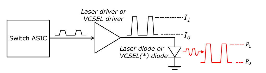
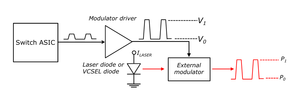
In general, there are two primary means to modulate an optical carrier:
P. Ossieur. “Introduction to Optical Communication Systems From VCSELs, integrated photonics to coherent solutions” ISSCC 2026
Direct Modulation - Modulate an optical signal by turning a laser source (VCSELs and DFBs) on and off with an electrical signal
 P. Ossieur. “Introduction to Optical Communication Systems From VCSELs, integrated photonics to coherent solutions” ISSCC 2026
External Modulation - Modulate a continuously running laser source through an external modulator that alters the optical properties of the material in some way in response to an electric field (electro-absorption, electro-optical, etc).
My comprehensive optical communication post broadly covers these two major modulation schemes:
IM-DD in pluggable transceivers has been the workhorse of data center networking for decades due to low cost, low power, and relative simplicity. However, high-speed electrical signals that travel between the ASIC and transceiver on copper are facing signal integrity challenges that makes long reach challenging.
Source: E. Temporiti. “VCSEL-based Solutions: Components, Circuits and Integration” ISSCC 2026
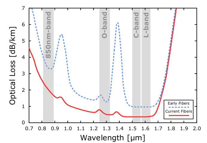
Depending on the distance the data travels, optical communications uses four primary optical bands to transport data. Rules of thumb include:
- Use 850nm directly modulated VCSELs for short reach (i.e. within a tray)
- Use O band for mid-reach datacom & CPO (scale-up and scale-out)
- Use C and L band for telecom & coherent long-haul (scale-across)
Since this post focuses on CPO for scale-up, we’ll mostly cover the options for external modulation in O-band. Coherent optical is its own complex beast and will be left out.
CPO: From Pluggable Modules, Scale-out, to Scale-up
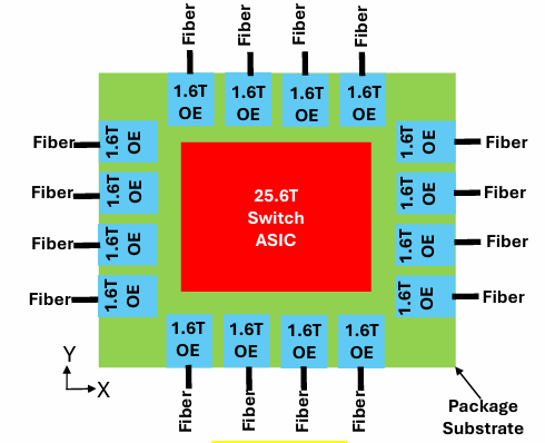
Source: J. Lau. “Advanced Packaging for Chiplets, Heterogeneous Integration, and Co-Packaging Optics” ECTC 2026
The purpose of CPO is to minimize power dissipation and the distance signals travel on copper due to reach limits at high frequencies. CPO performs the E-O and O-E domain conversion as close to the ASIC as possible to carry the data efficiently between chips in the optical domain. CPO engines also enable lighter SerDes circuits that don’t need as sophisticated, power-hungry DSP to drive and correct signals over long copper distances.
CPO was originally pitched for scale-out switch trays to overcome the crowded beachfront usage of front-panel faceplates due to DSP-based pluggable transceivers. CPO switches are connected directly to networking switch ASICs, such as Broadcom’s Tomahawk, Cisco’s Silicon One, or Nvidia’s Spectrum-X/Quantum-X. Note that CPO is not widely deployed in scale-out as of Sep 2026, but is beginning to see early, limited deployment.
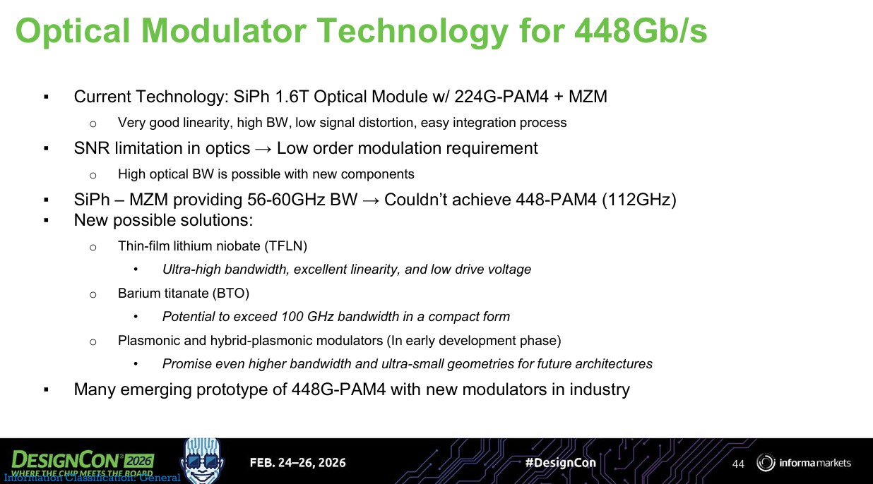
Source: H. Cirit. “448Gb/s Challenges for Scale Up and Scale Out Applications” DesignCon 2026
At DesignCon 2026 in February, Halil Cirit, AI Architect at Meta, noted that the current 224G/lane building blocks are 1.6T Optical Engines with 8 × 224G-PAM4 O-band MZM SiPh. Mach-Zehnder Modulators (MZM) are broadband devices, generally thermally robust, have a mature manufacturing ecosystem, and have sufficient area in large 51.2T/102.4T switch ASIC form factors. Overall, this switch has very good linearity, low distortion, and easy to integrate.
However, given the massive AI data needs, CPO is emerging as the main switch solution in scale-up domains to connect massively parallelized GPUs. Porting this technology from scale-out to scale-up faces several challenges for boosting data rate and integrating alongside xPUs, including:
- BW limits of SiPh (~56 - 60GHz) - this is right at the limit of 224G PAM4 signals with a Nyquist frequency of 56GHz
- Beachfront limits of ASICs competing with HBM and power modules
- Thermal characteristics of the hot GPU
- Reliability and serviceability of underlying components over the lifetime of the compute / switch tray
As a result, porting existing scale-out solutions to scale-up requires a fundamental rework of the standard modulator architecture and the underlying materials. On the photonics side, the two most promising modulators are ring modulators and electro-absorption modulators due to their compact size.
CPO addresses the consensus bottleneck of scale-up BW in AI data movement, but should be evaluated in the context of several other factors that can constrain data movement:
- New, much larger model architectures and sparse MoE parallelism can potentially bottleneck data movements in the scale-out domain
- Network contention can potentially leave compute underutilized. As OpenAI alluded to, high latency and network contention of single values that need to traverse scale-up / scale-out switches can hold up an entire parallel computation. Network contention is more destructive to spatial/dataflow architectures than temporal ones like Rubin.
- The electrical domain can potentially bottleneck optical modulator performance for 448Gbps+. In order words, you can have the fastest, holy grail optical modulator and PD, but their performance is wasted if the driver / TIA can’t drive / detect signals fast enough. Often times, the EIC driver bottlenecks BW.
Though scale-up BW is still the consensus bottleneck now, all three considerations are important to effectively scale together to handle future unpredictability of future model architectures and sparse MoE workloads that can escape the scale-up domain.
Major Components in CPO
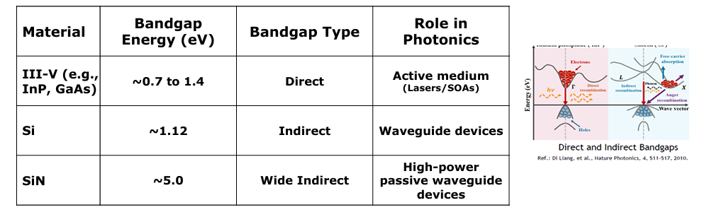
Source: C. Shih. “Silicon Photonics Platform for Next Generation HPC Technologies” ISSCC 2026
The reason all photonic components aren’t generally monolithically integrated is because Si is a poor generator of light. Si has an indirect bandgap where electron-hole recombination requires momentum conservation via a phonon alongside energy release as a photon. Si lasers are considered a “holy grail” laser.
As a result, O-band optical communications often disaggregates light generation from light manipulation because materials are often specialized for one of these purposes. Group III-IV semiconductors such as InP or GaAs only need an energy transfer to generate light. However, those materials have poor passive optical losses compared to Si and Si3N4. Furthermore, the processing steps for those materials tends to be incompatible with CMOS processing for EICs.
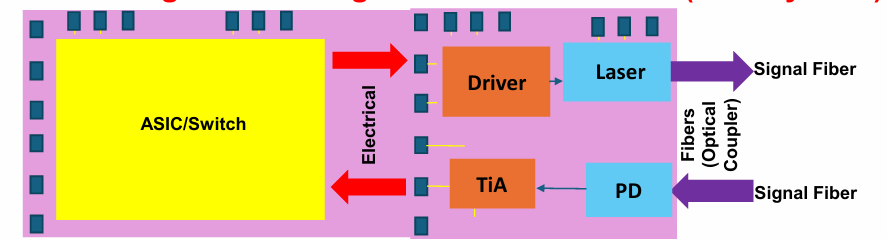
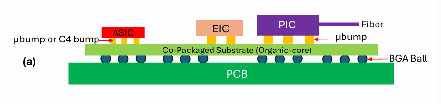
Source: J. Lau. “Advanced Packaging for Chiplets, Heterogeneous Integration, and Co-Packaging Optics” ECTC 2026
In the early days of CPO, blocks were distinct chiplets and 2D integrated on a common interposer to minimize the interconnect distance between chiplets. The transmit side consists of the following blocks:
- EIC Driver - Amplifies the electrical signal to the external modulator / directly modulated laser
- Laser - Provides the carrier optical signal to carry modulated data at a specific wavelength. For O-band, this laser can be coming from an external ELSFP / OSFP source coupled into an external modulator, or an externally modulated DFB laser (EML)
- PIC - The photonic integrated circuit that contains the passive optical waveguides and external modulator
- Fibers - Carries the optical signal through single-mode fibers. Fibers conventionally interface with the PIC via fiber array units (FAUs) utilizing V-groove arrays and edge or grating couplers.
The receive side requires the following:
- Photodetector - typically a PIN diode that converts optical signals to electrical current
- Transimpedance amplifier (TIA) - amplifies this electrical current to an electrical voltage
Packaging Options and Challenges
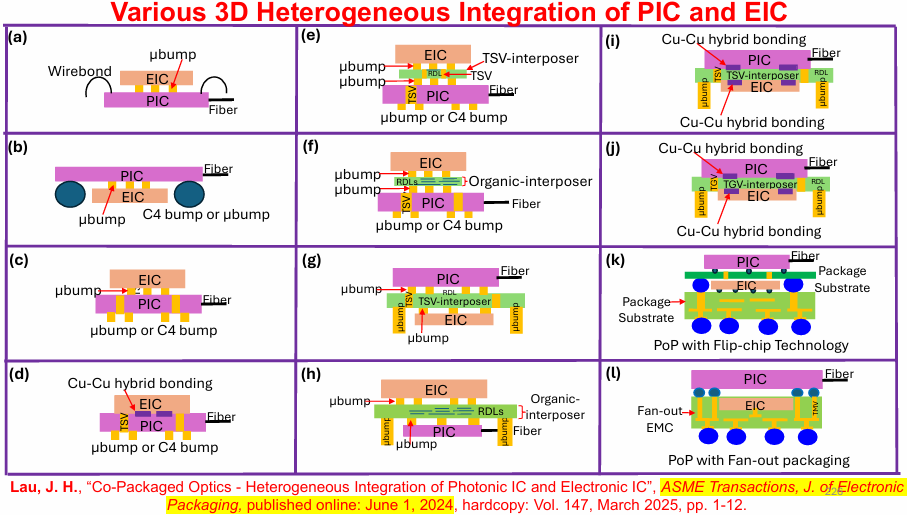
Source: J. Lau. “Advanced Packaging for Chiplets, Heterogeneous Integration, and Co-Packaging Optics” ECTC 2026
Optical packaging is the single largest cost and throughput bottleneck in post-silicon assembly at high volumes.
There is a host of 2.5D and 3D complex integration options to control light from an external laser source. Here we see 12 different integration techniques for PIC, EIC, and interposer. Some observations:
- Option c is the most common near-term implementation because it shortens electrical paths between EIC and PIC as much as possible. This helps minimize parasitic capacitance and inductance between the driver, TIA, and optical modulators / photodetectors
- Cu-Cu hybrid bonding is becoming increasingly mandatory for high-speed connections. The EIC driver/receiver BW is often limited by the parasitic capacitance the μbump inherently contains (10’s fFs). Hybrid bonding of critical connections will be mandatory to scale data throughput.
- Some configurations place the EIC and PIC on opposite sides of a shared interposer. These are used for complex routing or multi-chiplet bridging, but adds cost, assembly steps, and thermal resistance
Major Packaging Challenges: Yield and Precision Coupling
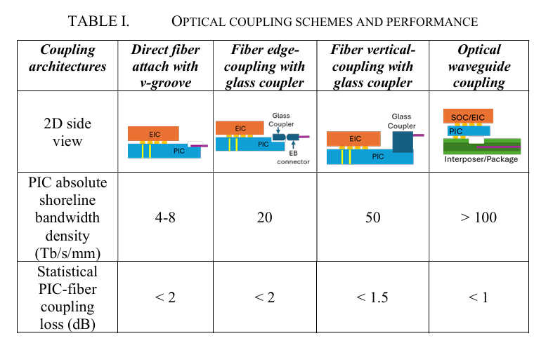
Source: Z. Zhang et al. “Multi-channel and multi-scale Optical Performance for a Detachable Edge-Coupling Connector with a Glass Coupler and Expanded Beam in CPO” ECTC 2026
Optical is highly sensitive to any manufacturing and packaging assembly mismatches. Optical signals really do not like to see jagged edges or discontinuities in the waveguide and interfaces that can cause optical losses and scattering, affecting laser characteristics.
Packaging presents several practical challenges to manufacture CPO switches at scale:
Manufacturing tolerance of optical coupling. Attaching fiber arrays units (FAUs) to photonic packages with nanometer alignment tolerances at volume is a big challenge.
- Detachability is a critical feature that help add to serviceability should CPO units fail in the field. Two major options include:
- Direct fiber attach with v-grooves - popular for legacy optical transceivers because they are simple to align. However, these require a thick fiber cable permanently dangling that take up a lot of beachfront area.
- Fiber edge-coupling with glass coupler - becoming more popular for detachability, allowing for full assembly and testing of the CPO module before being plugged in.
- Bonding Yield. Hybrid bonds are almost mandatory for high-speed 448Gbps+ signals, but have inherently limited yield and should be limited only to necessary connections. Unfortunately, hybrid bonding is very unforgiving with the most mature version, W2W at 98-99% per assembly and D2W at ~90-95% per assembly. More specific yield data is not publicly available and locked behind NDAs, and I think is mainly responsible for a lot of unfounded optimism regarding the technology readiness of hybrid bonding.
- Thermal Management. The CTE mismatch can create shearing / strain stresses on bumps and packaging materials. Glass is particularly sensitive due to its relatively low CTE compared to Si that places stress on the bumps
- Lack of Standardization. The electrical domain has a very well defined set of tool flows and standards, but optical does not have that and almost feels like the “wild west” at times. Major organizations such as OIF help define a common set of standards such as module form factors, but these are mostly contained at the component level, not the system level.
Packaging Examples
Three major SiPh foundry examples include TSMC, GF, and Intel as the main commercial foundries, and AIM Photonics as the main R&D one.
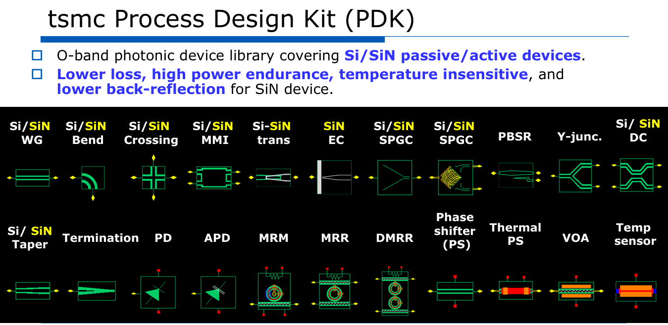
Source: C. Shih. “Silicon Photonics Platform for Next Generation HPC Technologies” ISSCC 2026
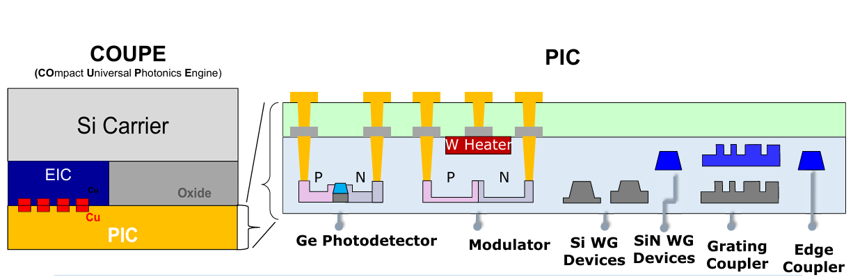
- TSMC COUPE (Compact Universal Photonics Engine) is the commercial benchmark for high volume SiPh packaging.
- The COUPE PDK contains a suite of photonic devices including Si/SiN waveguides, splitters, tapers, MRRs, PD, and temp sensors.
- TSMC’s SoIC-X 3D hybrid bonding is used to connect EIC and PIC, making it the default for Broadcom’s Tomahawk 6 and NVIDIA’s switches.
- However, COUPE locks vendors into their ecosystem and relies on external laser sources coupled in with grating couplers. Primary high-volume suppliers are Lumentum, Coherent, and Sumitomo Electric.
Source: A. Dasgupta et al. “Detachable Glass Waveguide Connector for Co‑Packaged Optics on Silicon Photonics platform with <1.5 dB/Facet Passive Coupling and 280 mW Power Handling” ECTC2026
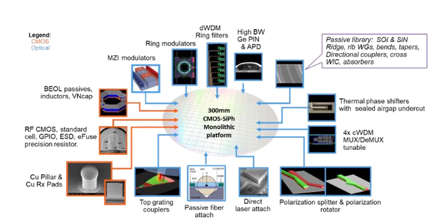
Global Foundries FOTONIX / SCALE - Unlike pure-play optical foundries, GF is positioned to enable monolithic CMOS-SiPh integration where the EIC and optical circuits are fabricated on the same 300mm Si wafer. In early 2025, it announced a $575M investment in an advanced packaging, testing, and manufacturing facility in Malta, NY to be built in multiple phases. GF has two main product lines:
 Source: Youtube
- FOTONIX - built on a 45nm RF SOI process that supports both CWDM and DWDM with all electrical and optical components available in the PDK. Their Gen 2 SiPh platform is proven up to 200G / λ with a clear path to 400G / λ.
- SCALE - the advanced packaging platform that physically packages the FOTONIX die into the CPO engines that are compliant with standard MSAs. It contains their proprietary fiber attach topologies, including V-groove passive alignment arrays and detachable glass/fiber connectors
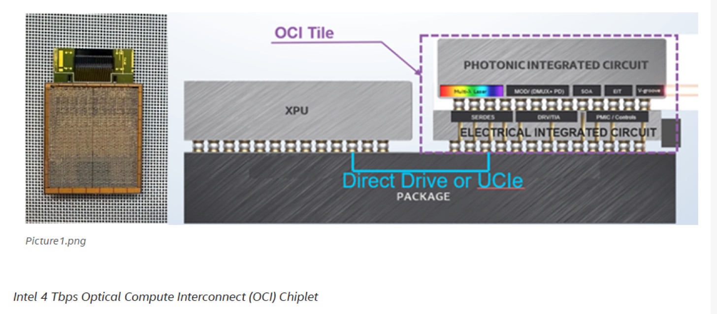
- Intel Silicon Photonics - The most integrated approach, Intel’s OCI is positioned around heterogeneously integrated InP lasers bonded directly on the Si Wafer.
- The Optical Compute Interconnect (OCI) tile consists of two parts:
- PIC, with hybrid InP lasers, SOAs, MRM, GE photodetectors, and passives
- EIC: High-speed SerDes, drivers, TIAs, PMICs, TSVs
- This approach is truly fully integrated and a radical departure from competitors that rely on external, off-package lasers. However, it faces several engineering challenges for controlling laser heat dissipation that requires aggressive cooling.
 Source: D Harame. “Weaving the Photonic Fabric: EPDA for Chiplet AI Systems” DAC 2026
- The Optical Compute Interconnect (OCI) tile consists of two parts:
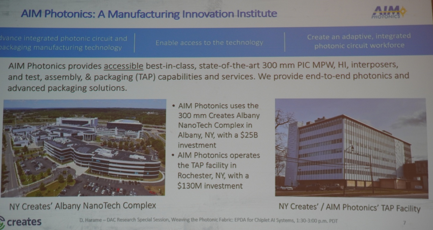
- AIM Photonics is a well known photonics foundry primarily focused on R&D academia, defense, and early-stage prototyping, rather than high-volume commercial manufacturing. You won’t find AIM photonics manufacturing the CPO engines at volume; it incubates such technologies for commercial production.
CPO Switch Examples
Notable CPO options include NVIDIA Quantum-X Photonics, Marvell/Celestial Photonic Fabric, and Broadcom TH5 and TH6. I covered NVIDIA and Marvell’s approaches in further detail, along with the physics of these modulators:
Two major CPO switch solutions include:
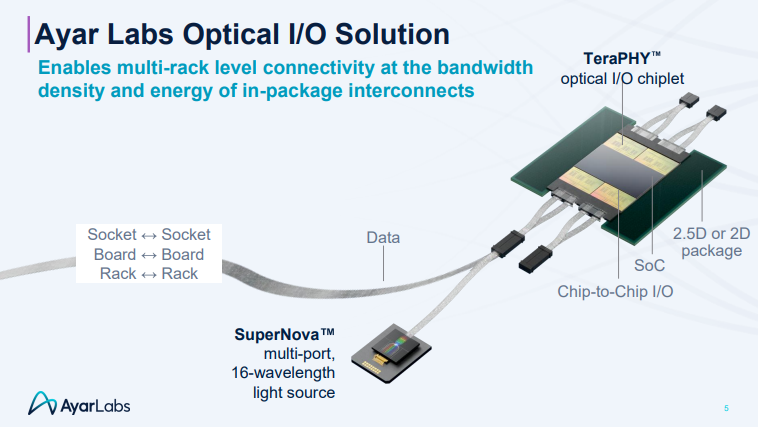
Source: V. Stojanovic. “A UCIe Optical I/O Retimer Chiplet for AI Scale-up” Hot Chips 2025
- Ayar Labs - Rather than building closed, proprietary networking switches/ OEs, Ayar Labs is positioned as the open, protocol optical I/O chiplet platform for scale-up to extend GPU-to-GPU fabrics like NVIDIA NVLink with uniform latency. Ayar Labs relies on high volume manufacturing across multiple vendors to lower single vendor lock-in risk.
- Ayar Labs was founded in 2015 as a spin out of a multi-year DARPA research collaboration between MIT, UC Berkeley, and CU boulder to commercialize silicon photonics and optical chiplet technologies.
- Ayar Labs has two main products:
- TeraPHY - an electrical-optical PHY chiplet placed side by side with host logic dies on a shared 2.5D interposer.
- It primarily uses MRMs and Ge photodetectors on GF’s monolithic 300mm platform previously discussed.
- TeraPHY is protocol agnostic, so it performs the E-O conversion no matter whether the data is PCIe, CXL, UCIe, etc.
- It supports 8 Tbps of bi-directional BW, which is top tier compared to 16x PCIe6 that caps out at ~1Tbps.
- SuperNova - the multi-wavelength continuous wave O-Band laser in an ELSFP form factor
- Supernova supports 8 to 16 wavelengths per optical port across 16 ports for 256 total optical channels power port
- TeraPHY - an electrical-optical PHY chiplet placed side by side with host logic dies on a shared 2.5D interposer.
- Note that unlike NVIDIA that is closed, proprietary, and vertically integrated, Ayar Labs maximizes interoperability and provides the plumbing, similar to ARM or Synopsys. Ayar does NOT make the host ASICs, full network switches, and pluggable optical transceivers. Vendors buy their TeraPHY and SuperNova and system integrate themselves.
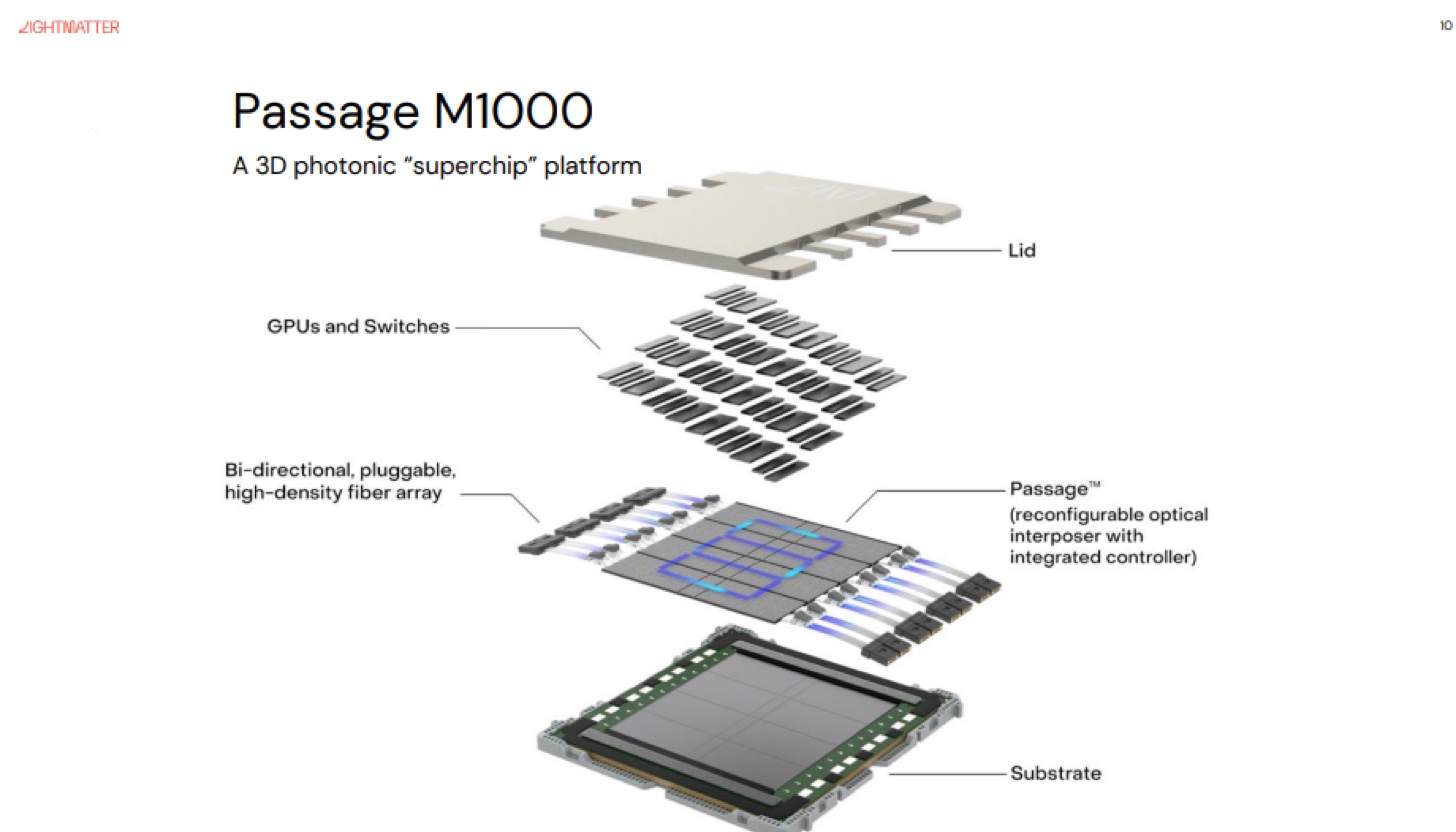
Source: D. Bunandar. “Passage M1000 A 3D Photonic Interposer for AI” Hot Chips 2025
- Lightmatter. Unlike 2.5D packaging that Ayar Labs and Intel OCI do, Lightmatter does 3D integration of chips by mounting compute dies directly on top of a photonic interposer. This completely eliminates the shoreline density limits and caps.
Their flagship platform, Passage, stitches four tiles reticles across a 300mm wafer to deliver ~114-256Tbps of aggregate optical interconnect throughput. These optical switches are SW programmable.
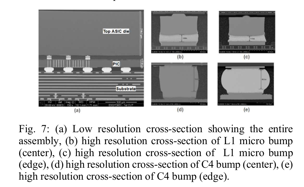 Source: S. Ahmed et al. “Advancing Interconnect Performance and Reliability with Innovations in 3D Photonic Integration Packaging and Fiber Coupling” ECTC 2026
- This is a cross section of the Passage interposer. The middle PIC contains all of the photonic devices (waveguides, modulators, PDs and TSVs). The PIC connects to the top ASIC die with with dense L1 bump arrays and connects to the substrate underneath with C4 bumps.
- Passage relies on MRMs which fundamentally faces thermal control challenges. Lightmatter integrates closed loop thermal tuning circuitry to lock each ring’s resonance into its appropriate laser wavelength. However, in the future, these rings face several thermal challenges for unpredictable workloads and higher compute power, especially when the large data movement it enables adds to compute heat.
Part 2: Light Manipulation: PIC Modulator Material Options
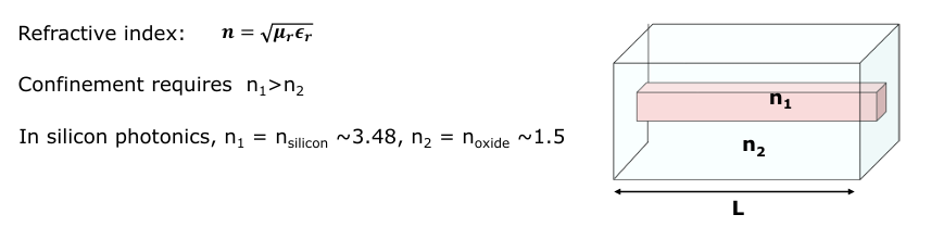
Source: F. Aflatouni. “Silicon photonics-based solutions: components, circuits, and integration” ISSCC 2026
Now lets talk about the two workhorse technologies for light manipulation, Silicon-on-Insulator and Si3N4. Note that SiPh is linguistically used as the umbrella term lumping together all technology options within CPO, though SiPh, strictly speaking, refers to silicon-on-insulator in CPO.
Recall that in standard optical waveguides, the waveguide material has a higher refractive index than the surrounding oxide to ensure total internal reflection, containing the light within the waveguide.
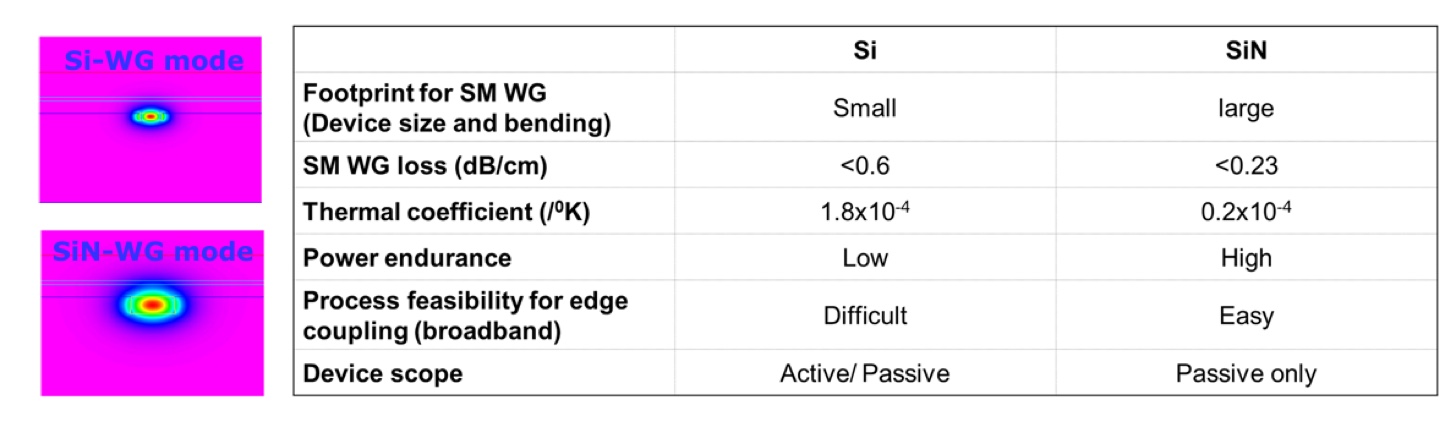
Source: C. Shih. “Silicon Photonics Platform for Next Generation HPC Technologies” ISSCC 2026
Modern workhorse SiPh relies on two materials: Silicon-on-Insulator, and Silicon Nitride (Si3N4)
- Silicon-on-Insulator (SOI) integrates optical components onto a Si chip using standard CMOS technology.
- Silicon modulates light via free-carrier plasma dispersion with MZM and ring modulators. Epitaxial GeSi supports EAM modulation and PIN junctions for photodetectors.
- Silicon-on-insulator has been the go-to material of choice for 224G PAM4 faces, but faces several scaling challenges for future CPO switches:
- The BW of SOI modulators is limited to 56 - 60 GHz, barely being able to handle 224G data rates operating at a Nyquist frequency of 56GHz. This doesn’t make Si the ideal material for high-speed modulation at 448Gbps.
- Two-photon absorption (TPA) inherently limits laser power coupled in.
- Silicon Nitride (Si3N4) is an insulator material that is transparent from the visible spectrum (400 nm) out to the mid-infrared spectrum (4000 nm)
- Si3N4 is well-suited for passive routing for the following reasons:
- Low-loss optical waveguides effectively handles high-power lasers
- Massive bandgap of 5 eV completely eliminates TPA
- Low thermo-optic coefficient (7.5x lower than Si) allows for good thermal stability when next to hot GPUs
- Efficient fiber-to-chip edge coupling due to low refractive index
- However, Si3N4 is a difficult material to modulate/detect light with for two reasons:
- It cannot host PN junctions or free carriers since it is an insulator
- Poor active tuning range to control light with thermo-optic heaters due to a lower thermo-optic coefficient
- Si3N4 is well-suited for passive routing for the following reasons:
Both Si and Si3N4 are commonly co-integrated in two layers on top of each other that serve different purposes:
- Si / TFLN / InP layer handles the modulation
- Si3N4 handles the low loss, high-power routing and performs WDM multiplexing
- Ge / InP layer handles photodetection
One of the most challenging problems in photonic integrated circuit design is moving light vertically between layers. Grating couplers are dominant for off-chip coupling. Adiabatic directional couplers are often used for internal chip coupling between layers where waveguides “taper” to force light to move in a vertical direction to a nearby tapered waveguide as well. Optical TSVs with 45o mirrors are an emerging trend to transport light with several excellent ECTC 2026 papers. However, optical TSVs have very stringent alignment and cleaning requirements.
Photonic Design Automation
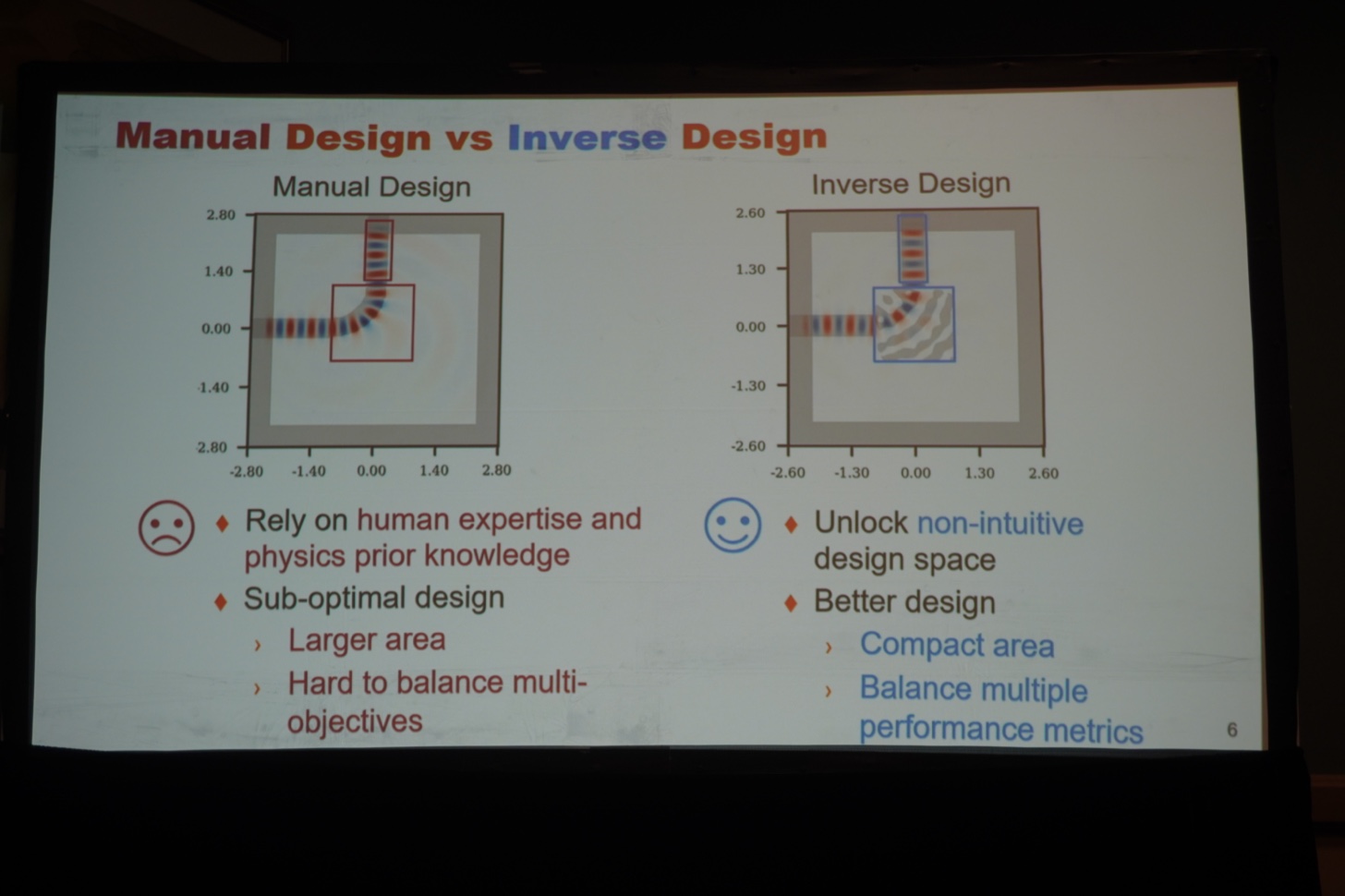
Source: H. Zhou. “End-to-end Physical Design Automation Flow for Yield-Optimized Inverse-Designed Large-Scale Electronic-Photonic Integrated Circuits” DAC 2026
Light does not like sharp bends and waveguides have losses due to surface roughness. Routing light from a coupled-in laser to the modulator and FAU requires computationally intensive SW to model optical leakage and verify overall functionality. Ansys Lumerical is a dominant player in the CAD SW.
Photonic design automation such as inverse design can also be employed to aid in optimizing certain sections. This has potential use, but is generally not relied upon on because generated structures generally suffers from high variability to process variation. Generated structures take a long time to optimize and often do a good job at generating compact structures in ideal environments,. However, these structures are often unsatisfying on other key performance metrics over manufacturing variability.
Emerging Directions for CPO Modulation
I’ll highlight a few emerging approaches for scaling data rate to 448Gbps, one is that becoming commercially viable, and another that is a “holy grail”. (Note that InP EMLs is the most widely deployed material for high-speed optical modulation in pluggables and will be discussed in the next section):
- TFLN - Thin-film Lithium Niobate (LiNbO3) - widely recognized as the most promising frontrunner for next gen 224G/448G per lane modulators
- Lithium Niobate (LiNbO3) is not new and has been the workhorse of telecom fiber-optics because of no chirp and high reliability. However, legacy devices are quite large and need high drive voltage not immediately suitable for CPO.
- In TFLN, a 300-500nm film of lithium niobate is bonded on a SI substrate. TFLN modulates light with the Pockels effect (or the linear electro-optic effect) where the refractive index changes linearly and almost instantaneously to an applied electric field. This is is because, unlike Si’s free-carrier depletion, there are no physical electrons or holes moving around.
- TFLN has several advantages well-suited for CPO:
- Tight electrode confinement - electrodes are 1-2um apart
- Very low half-wave voltage (Vπ * L ~ 1.5 - 2.5 V*cm) to be driven by LV drivers
- Can reach BWs up to 100-145GHz
- However, TFLN posts a major contamination risk in front-end fabs:
- Lithium is not compatible with CMOS fabs because lithium poisons silicon gate oxides and residual traces on equipment can corrupt batches of multi-billion dollar CMOS wafers.
- For this reason, tier 1 fabs like TSMC won’t integrate Li into their front-end CMOS line for good reason.
- As a result, TFLN optical modulators are fabricated in specialized photonic foundries physically separated from mainstream CMOS lines and then combined together with Si chips at the end.
- Key players include:
- Hyperlight - Commercial pure-player partners with UMC and Wavetek
- NanoLN - Provides wafers with lithium niobate on insulators
- Barium Titanate (BTO) - widely considered a “holy grail” material for CPO
- BTO us a ferroelectric perovskite oxide with a very high Pockels tensor coefficient, enabling massive optical phase shifts with a small shift in electric field
- BTO has several advantages:
- Very low drive voltage (Vπ * L ~ 0.2 - 0.5 V*cm), enabling direct drive from raw CMOS levels without power hungry amplifiers/drivers
- Tiny footprint
- Compatible with CMOS fabs
- However, BTO is much less mature for the following reasons:
- It requires uniform, defect free BTO films to be grown with molecular beam epitaxy
- Higher waveguide optical loss (2-5dB / cm) due to grain boundaries
- BTO is ordinarily ferroelectric before its Curie temperature of 120 °C and needs electrical poling to maximize the electro-optic effect
- BTO is being actively researched by IBM/ETH Zurich, Lumiphase (a spinout of IBM/ETH Zurich) and imec.
- In short, BTO has tremendous potential potential to exceed 100GHz in a compact form factor with low drive voltages and higher frequency. However, don’t forget that it also requires a comparable EIC to drive it / receive it fast enough.
There are several other potential materials such as organic electro-optic (OEO) polymers, plasmonic, and hybrid-plasmonic modulators that are being actively researched.
Part 3: Light Generation - Lasers / Light Sources
External lasers specifically used for Silicon Photonics (SiPh) and CPO/NPO primarily use CW-WDM MSA architectures where continuous-wave (CW) light is fed to off-chip modulators.
After the paywall the following topics will be further discussed:
Part 3: Light Generation - Laser Options
- 🔒InP - The Laser Substrate Material of Choice
- 🔒Distributed Feedback Laser (DFB)
- 🔒Other O-Band Lasers (EML, Hybrid, Quantum Dot, multi-λ)
- 🔒Important Considerations in Laser Selection
- 🔒Laser Form Factors (OIF ELSFP, OSFP)
- 🔒Wavelength Division Multiplexing (WDM)
Part 4: EIC Architecture Options
- 🔒Driver Design Considerations and Topologies for MZM, MRM, and EAM
- 🔒TIA Design Considerations
- 🔒Higher-Order Modulation & Simultaneous Bi-Directional Transmission
- 🔒FEC options
第二部分:中文深度解读
一句话定位
这不是一篇论文,也不是一篇新闻,而是一份系统架构师视角的 CPO 选型地图。作者把 224Gbps 及以上速率的共封装光学(CPO)拆成四层——封装架构、PIC 材料、激光光源、EIC 电路——每一层给出”有哪些选项、各自的取舍是什么、谁在量产”。它不提供新结果,提供的是把散落在 ISSCC / ECTC / DAC / Hot Chips / DesignCon 各处的碎片拼成一张脑图。
公开部分(付费墙之前)覆盖 Part 1 封装架构与 Part 2 光操控材料全篇,以及 Part 3 激光部分的引言;Part 3 后半(InP/DFB/EML/量子点/激光选型/ELSFP 形态/WDM)与 Part 4(driver/TIA/高阶调制/FEC)在付费墙后,本站不转载,仅在下文列出其目录供你判断是否需要订阅。
一、作者的分析坐标系:三个切分
这篇文章真正有价值的地方不在信息量,而在于它给出的三把切刀。理解了这三条,后面所有零散的技术讨论都能归位。
1.1 光产生(Light Generation)vs 光操控(Light Manipulation)
作者自己承认:这两个领域的材料经常被混为一谈,”我自己也犯过这个错”。原因是 InP 既能发光也能调制,于是大家习惯把”光”当成一件事。
但对 O-band CPO 而言,这条切分几乎是全部架构设计的前提:
- 硅是糟糕的发光体——间接带隙,电子-空穴复合需要声子参与动量守恒,纯硅激光至今是”圣杯”级别的难题。
- 于是发光必须交给 III-V 族(InP、GaAs),它们的代价是:无源光学损耗远高于 Si 与 Si₃N₄,且工艺与 EIC 的 CMOS 前道不兼容。
- 结论:把”产生”与”操控”物理拆开——激光外置,通过 CW-WDM MSA 架构把连续光送入片外调制器。这不是设计偏好,是物理约束逼出来的唯一解。
这条推理链解释了后面几乎所有的产业现象:为什么 GF 要强调 monolithic CMOS-SiPh、为什么 Intel OCI 要”激进地”把 InP 激光异质集成到硅晶圆上(并因此必须面对激光散热)、为什么 ELSFP 这种外置激光模块形态会成为标准件。
1.2 Scale-out vs Scale-up
CPO 的出身是 scale-out 交换机:可插拔光模块挤满了前面板(beachfront),CPO 把光电转换搬到交换 ASIC 旁边(Broadcom Tomahawk、Cisco Silicon One、NVIDIA Spectrum-X / Quantum-X)。
但真正的增量在 scale-up——连接大规模并行 GPU。作者明确点出移植不是简单放大,四条挑战:
| 挑战 | 具体含义 |
|---|---|
| SiPh 带宽上限 56–60 GHz | 224G PAM4 的 Nyquist 频率正好是 56 GHz,余量几乎为零 |
| ASIC 的 beachfront 竞争 | 要与 HBM、电源模块抢边缘面积 |
| 热环境 | 紧贴高温 GPU,而非温度可控的交换机托盘 |
| 可靠性与可服务性 | 要在计算托盘的整个生命周期内维持 |
由此,MZM(马赫-曾德尔调制器)虽然在大尺寸 51.2T/102.4T 交换 ASIC 上有足够面积、线性好、热稳定、工艺成熟,却在 scale-up 里显得太大——环形调制器与电吸收调制器(EAM)因体积紧凑成为两个最有希望的替代。
1.3 组件级标准 vs 系统级标准
作者用了一个少见的带情绪表述:光域”有时候感觉像西部荒野“。电域有完整定义好的工具流与标准,光域没有。OIF 这类组织定义的是模块形态(ELSFP、OSFP)这类组件级标准,系统级标准缺位。
这条判断的实用价值在于:它解释了为什么不同厂商的 CPO 方案之间几乎无法互换,也解释了为什么”TSMC COUPE 锁定生态”会成为一个被明确写出的缺点。
二、因果骨架:为什么 CPO 的瓶颈清单里几乎没有”光”
把全文按因果顺序重排,会得到一条很清晰的链:
1
2
3
4
5
6
7
8
9
10
11
12
13
14
15
物理约束        Si 不发光(间接带隙)
                SiPh 调制带宽 56–60 GHz
                双光子吸收(TPA)限制耦合激光功率
        ↓
架构约束        激光必须外置(或异质集成并承担散热)
                EIC 与 PIC 必须分离制造、后段拼装
                高速链路必须用 Cu-Cu 混合键合(μbump 寄生电容 ~10s fF)
        ↓
制造约束        纳米级光纤耦合公差
                混合键合良率(W2W 98–99%、D2W 90–95% 每次装配)
                CTE 失配导致凸点剪切应力(玻璃尤其敏感)
        ↓
生态约束        缺系统级标准,厂商锁定
        ↓
结论            不存在"最优解",只有一张选项表
这条链最有信息量的地方是它的终点:CPO 的瓶颈几乎全是封装、良率、测试、驱动电路——没有一条是”光学器件本身不够好”。这跟外界对 CPO 的直觉(认为难点在光子学)恰好相反。
三、分层拆解
3.1 封装与集成层
作者给出了 12 种 PIC / EIC / interposer 的集成方案,并点出近期的实际选择:
- 选项 c 是近期最主流的实现——把 EIC 与 PIC 之间的电学路径压到最短,从而最小化驱动/TIA 与调制器/探测器之间的寄生电容与电感。
- Cu-Cu 混合键合正变得越来越必要:EIC 驱动/接收的带宽经常被 μbump 固有的寄生电容限制(数十 fF 量级)。要提升数据吞吐,关键连接上的混合键合是”mandatory”。
- 把 EIC 与 PIC 放在同一 interposer 两侧的配置存在,用于复杂布线或多 chiplet 桥接,代价是成本、装配步骤与热阻。
3.2 材料层:两类材料的联合体
| 材料 | 角色 | 优势 | 致命短板 |
|---|---|---|---|
| SOI(绝缘体上硅) | 调制 | CMOS 兼容;自由载流子等离子色散效应,支持 MZM 与环形调制器;外延 GeSi 支持 EAM 与 PIN 探测器 | 带宽锁死 56–60 GHz;TPA 限制耦合激光功率 |
| Si₃N₄(氮化硅) | 无源路由 / WDM | 低损耗波导可承高功率;5 eV 带隙彻底消除 TPA;热光系数比 Si 低 7.5 倍(紧邻热 GPU 时热稳定性好);低折射率带来高效光纤-芯片边缘耦合 | 绝缘体,无法承载 PN 结或自由载流子;热光加热器的调谐范围差 |
| Ge / InP | 探测 | — | — |
| TFLN(薄膜铌酸锂) | 调制(新锐) | 普克尔斯效应(线性电光,无载流子运动→近乎瞬时);电极间距 1–2 µm;Vπ·L ≈ 1.5–2.5 V·cm;带宽可达 100–145 GHz | 锂毒化硅栅氧,一线 CMOS 前道厂(含 TSMC)拒收;只能在专用光子代工线制造后段拼装 |
| BTO(钛酸钡) | 调制(圣杯) | Vπ·L ≈ 0.2–0.5 V·cm(可直接由裸 CMOS 电平驱动,省掉功耗放大器);footprint 极小;与 CMOS 厂兼容 | 需 MBE 生长无缺陷均匀薄膜;晶界导致 2–5 dB/cm 高损耗;居里温度 120 °C 需电极化;成熟度低 |
数字支撑:Si vs SiN 的定量对照
这篇文章(公开部分)极少给出对照表,而图 21 是其中一个例外,把 Si 与 SiN 的取舍量化了(来源:C. Shih, ISSCC 2026):
| 指标 | Si | SiN |
|---|---|---|
| 单模波导 footprint | 小 | 大 |
| 单模波导损耗 | < 0.6 dB/cm | < 0.23 dB/cm |
| 热光系数(/K) | 1.8×10⁻⁴ | 0.2×10⁻⁴ |
| 功率承受能力 | 低 | 高 |
| 边缘耦合可行性(宽带) | 难 | 易 |
| 器件范围 | 有源 + 无源 | 仅无源 |
两处值得记下的细节:
- 表中热光系数之比是 9 倍(1.8×10⁻⁴ vs 0.2×10⁻⁴),而正文写的是 7.5 倍。同一篇稿件内部的这处不一致提示:这类材料参数与口径强相关(波长、掺杂浓度、温度),引用时应同时给出条件,否则容易被当成常数。
- 损耗一行是 SiN 明显占优(<0.23 vs <0.6 dB/cm),但 footprint 一行 Si 明显占优。这正是”Si 负责调制、SiN 负责路由”分工的量化依据——只盯损耗一行会得出错误结论。
这一层的核心结论:Si 与 Si₃N₄ 不是竞争关系而是分工——Si(或 TFLN / InP)层负责调制,Si₃N₄ 层负责低损耗高功率路由与 WDM 复用,Ge / InP 层负责探测。真正难的是把光在层间竖直搬运:片外靠光栅耦合器,片内层间靠绝热定向耦合器,而带 45° 反射镜的光学 TSV 是新兴方向(对齐与清洁要求极严)。
3.3 生态与量产层
| 厂商 | 路线 | 关键事实 |
|---|---|---|
| TSMC COUPE | 2.5D + SoIC-X 3D 混合键合 | 商业化基准;PDK 含 Si/SiN 波导、分束器、锥形耦合、MRR、PD、温度传感器;成为 Broadcom TH6 与 NVIDIA 交换机的默认;锁定生态,激光靠光栅耦合外置,主要供应商 Lumentum / Coherent / Sumitomo Electric |
| GF FOTONIX / SCALE | 单片 CMOS-SiPh 集成 | 同一 300mm 硅片上做 EIC 与光路;45nm RF SOI,支持 CWDM+DWDM,Gen2 已验证 200G/λ 并有通往 400G/λ 的路径;2025 年初宣布 5.75 亿美元在纽约 Malta 建先进封装/测试/制造厂;SCALE 是符合 MSA 的封装平台,含 V 型槽被动对准与可拆卸玻璃/光纤连接器 |
| Intel OCI | 异质集成 InP 激光键合到硅晶圆 | “最集成”的路线,激进地摆脱外置激光;代价是激光散热需激进冷却 |
| AIM Photonics | R&D / 学界 / 国防 / 早期原型 | 不做量产,孵化技术 |
| Ayar Labs | 开放协议的光 I/O chiplet | 2015 年从 MIT / UC Berkeley / CU Boulder 的 DARPA 合作项目分拆;TeraPHY 与 host logic 并排放在 2.5D interposer 上,用 GF 单片 300mm 平台的 MRM 与 Ge 探测器;协议无关(PCIe / CXL / UCIe 皆可);8 Tbps 双向(对比 16× PCIe6 的约 1 Tbps);SuperNova 是多波长 CW O-band 激光(ELSFP 形态,每光口 8–16 个波长 × 16 口);定位是提供”管道”,类似 ARM 或 Synopsys,不做 host ASIC 与整机 |
| Lightmatter | 3D 集成(计算 die 直接放在光子 interposer 上) | 彻底消除 shoreline 密度上限;Passage 平台把四块 reticle 拼在 300mm 晶圆上,聚合光互连吞吐约 114–256 Tbps,光交换可软件编程;剖面显示中间 PIC 含波导/调制器/PD/TSV,向上靠密集 L1 凸点连 ASIC,向下靠 C4 凸点连基板 |
四、关键数字清单(可核查)
| 数值 | 含义 | 出处层级 |
|---|---|---|
| 1.6T 光引擎 = 8 × 224G-PAM4 O-band MZM SiPh | 当前 224G/lane 的构建块定义 | DesignCon 2026,Meta AI 架构师 Halil Cirit |
| 56–60 GHz | SiPh 调制器带宽上限 | 器件物理 |
| 56 GHz | 224G PAM4 的 Nyquist 频率 | 信号完整性基本关系 |
| ~10s fF | μbump 固有寄生电容 | 封装物理 |
| 98–99%(W2W)/ 90–95%(D2W) | 混合键合每次装配良率 | 作者给出的行业区间,更细数据在 NDA 内 |
| 5 eV | Si₃N₄ 带隙(消除 TPA) | 材料参数 |
| 7.5× | Si₃N₄ 热光系数低于 Si 的倍数 | 材料参数 |
| 1.5–2.5 V·cm(TFLN)/ 0.2–0.5 V·cm(BTO) | Vπ·L 半波电压-长度积 | 器件参数 |
| 100–145 GHz | TFLN 可达带宽 | 器件参数 |
| 2–5 dB/cm | BTO 波导损耗(晶界) | 材料参数 |
| 120 °C | BTO 居里温度 | 材料参数 |
| 8 Tbps 双向 | Ayar TeraPHY 单 chiplet 带宽 | 厂商公开 |
| ~1 Tbps | 16× PCIe6 的带宽(对比项) | 接口标准 |
| 114–256 Tbps | Lightmatter Passage 聚合光互连吞吐 | 厂商公开 |
五、我的评述:哪些判断经得起检验
5.1 全文最重要的一句,藏在 Part 1 的第三条里
作者在列举”可能制约数据搬移的其他因素”时写道:电域会先卡住 448Gbps 以上的光调制器性能——你即便拥有最快的”圣杯”调制器与光电探测器,只要 driver / TIA 跟不上,性能就是浪费,而 EIC driver 常常正是带宽瓶颈。
这一条把整篇文章的重心从光子学挪到电路与封装。而作者在 Part 2 结尾再次呼应:”别忘了 BTO 也需要一个同等水平的 EIC 才能足够快地驱动它”。前后两处呼应,说明这不是随口一提,而是他的核心判断。 对工程决策的直接含义:如果你的目标是 448G/lane,先看 driver 与 TIA 的带宽预算,再看调制器材料——顺序反了会走弯路。而 Part 4(driver 拓扑 / TIA 设计)恰好被付费墙挡住,这是公开部分最大的结构性缺口。
5.2 TFLN 的”锂毒化栅氧”不是技术细节,而是产业格局的解释
文中这条被一笔带过:锂会毒化硅栅氧,残留在设备上的痕迹可能毁掉整批数十亿美元的 CMOS 晶圆,所以 TSMC 这类一线厂不会把 Li 引进前道线;TFLN 调制器只能在与主流 CMOS 线物理隔离的专用光子代工厂制造,再在后段与硅芯片拼装。
这条约束解释了三个产业现象:为什么 Hyperlight 要绑 UMC 与 Wavetek、为什么 NanoLN 只卖”绝缘体上铌酸锂”晶圆而不做器件、为什么 TFLN 明明性能最好却在量产上落后于看起来更”平庸”的 SOI。
反过来看 BTO:它被称作”圣杯”的首要理由其实是”与 CMOS 厂兼容”,性能优异只是必要条件。可制造性才是充分条件——这是材料选型里最容易被工程师低估的一环。
5.3 “12 种集成方案、选项 c 是近期主流”透露的事实
短期内决定 CPO 成败的是封装工艺路线,不是调制器材料。这解释了一个反直觉的现象:TSMC COUPE 能成为 Broadcom TH6 与 NVIDIA 交换机的默认方案,靠的是 SoIC-X 混合键合与 PDK 生态,而不是它在光子器件上有什么独门绝技——它的激光甚至是外置的,靠光栅耦合器送进来。
5.4 Lightmatter 的 3D 路线里藏着一个自我指涉的负反馈
Lightmatter 用 3D 集成(计算 die 直接压在光子 interposer 上)彻底消掉了 shoreline 上限,代价是环形调制器(MRM)的热控制:需要闭环热调谐电路把每个环的谐振锁定到对应激光波长。作者点出的未来风险很关键——在不可预测的工作负载与更高算力下,尤其是当它自己带来的大规模数据搬移也变成热源时,这些环会面临更严峻的挑战。
换句话说:你为了解决散热与密度问题把光搬进 3D,结果光所承载的数据搬移本身又制造了新的热。这是一个自我指涉的负反馈回路,值得单独拎出来——它不是工程细节,而是路线选择的内在张力。
5.5 混合键合良率:全篇最有价值的一句”负面判断”
作者写得很直白:混合键合对高速 448Gbps+ 几乎不可避免,但良率天然受限且应只用在必要连接上;最成熟的形态 W2W 每次装配 98–99%、D2W 约 90–95%;更具体的数据不公开、锁在 NDA 里;而他认为这正是一批人对混合键合技术成熟度产生”不切实际乐观”的主要原因。
这句话的价值在于它是负面的、且出自业内人士之口。但使用时要注意两点边界:
- 这是每次装配的良率,不是最终模块良率。多次键合会累积,累积模型作者没有给。
- 这是判断而非数据。W2W 98–99% 这个区间的来源未标注,应作为”行业从业者的直觉区间”引用,不宜当作统计事实。
5.6 需要警惕的两处:逆设计(inverse design)与 TPA
- 逆设计:作者的态度是”有潜力,但一般不依赖”,理由是生成结构对工艺漂移的容忍度差、优化耗时长、只在理想环境中表现好。这是一个非常务实的评价——逆设计在文献里常常被吹捧,而产业界对它的迟疑正是”可制造性”问题。
- TPA(双光子吸收):文中把 TPA 列为 SOI 的短板(限制耦合激光功率),并在 Si₃N₄ 那一侧用”5 eV 带隙彻底消除 TPA”作为优势。但当”更高激光功率”与”更多波长(WDM)”同时推进时,TPA 究竟会不会成为系统级的硬墙,公开部分没有量化。这是一个被提出但未被回答的问题。
六、可采信度分层
| 层级 | 内容 | 理由 |
|---|---|---|
| 强(可直接采信) | 硅的间接带隙;SiPh 调制带宽 56–60 GHz;TPA 物理;Si₃N₄ 的 5 eV 带隙与热光系数;混合键合在高速链路中的物理必要性;TFLN / BTO 的 Vπ·L 量级 | 器件物理与材料常数,可独立核验 |
| 中(有来源,仍是企业自述) | Meta 对 1.6T = 8×224G MZM 的定义;TSMC COUPE 的 PDK 器件清单与客户关系;GF 的 200G/λ 与 5.75 亿美元投资;Ayar 的 8 Tbps;Lightmatter 的 114–256 Tbps | 均为 ISSCC / ECTC / DAC / Hot Chips / DesignCon 的公开陈述,基本可信但未经第三方复现 |
| 弱(作者个人判断,应作假设) | 混合键合良率”导致不切实际的乐观”;光域是”西部荒野”;逆设计”一般不被依赖”;选项 c 是”近期最主流” | 有行业直觉价值,但无数据支撑,不宜当事实引用 |
| 未含(付费墙) | Part 3 后半:InP 衬底材料、DFB、EML/混合/量子点/多波长、激光选型考量、ELSFP·OSFP 形态、WDM;Part 4:MZM/MRM/EAM 的 driver 设计与拓扑、TIA 设计、高阶调制与双向同传、FEC 选项;结论章 | 内容不在公开部分,本地未取得,不转载 |
七、这篇文章没有回答什么
这是解读里最该说清楚的部分。以下都是公开部分未涵盖、但对决策影响很大的缺口:
- 没有任何成本数字。全文反复强调”光学封装是后硅装配中最大的成本与吞吐瓶颈”,却没有给出一个美元量级——无论是每引擎成本、每 Gbps 成本,还是良率换算后的单位成本。对投资判断来说这是最大的空洞。
- 没有功耗数字。CPO 的核心卖点本应是 pJ/bit 能效,全文(公开部分)没有出现一个能耗数字,只有”更轻的 SerDes、不需要那么复杂耗电的 DSP”这种定性描述。
- 没有测试与老化数据。文中把”可拆卸性(detachability)”定位为现场失效时的可服务性,但没有展开测试时间、测试成本与老化筛选——而这恰恰是 CPO 从 demo 走向量产的另一半问题(参见站内 SENKO / Advantest / VIAVI 的模块级测试解读)。
- “224G 够不够用”其实没被回答。作者把”SiPh 带宽 56–60 GHz 刚好等于 224G PAM4 的 Nyquist 56 GHz”列为挑战,但余量为零并不等于不可用——实际系统会依赖 FEC 与前馈均衡。而 FEC 恰好被写在付费墙之后的 Part 4。所以这个最实际的问题,公开部分给不出答案。
- 作者的来源结构带来”会议议程偏差”。文首自述是 IMAPS 与 SiPh Symposium 的 media partner,全文材料主要来自 ISSCC / ECTC / DAC / Hot Chips / DesignCon。被会议讨论最多的技术,不等于量产占比最高的技术——这两者在本领域差距很大。
- 时点价值需要记下:作者明确说 CPO 在 scale-out 领域”截至 2026 年 9 月尚未广泛部署,刚开始出现早期的、有限的部署”。这句话把整篇文章的定位从”现状总结”校正为”面向 448G 的路线预判“,两者对投资的含义完全不同。
八、与站内其他文章的联系
| 站内文章 | 关联点 |
|---|---|
| 从 SerDes 到光纤:可交互的 NPO 光电链路实验室 | 本文反复强调”电域先卡住光”,那篇给出了可动手调参的链路预算与均衡视角 |
| 华为推动 OIF NPO 标准化与首个 7.2T NPO 模块 | 与本文”组件级标准已有、系统级标准缺位”的判断直接呼应:OIF 定义模块形态,但系统级仍空白 |
| 通往 CPO 之路上的 NPO:NewPhotonics NPC50503 解读 | 该方案的”以光域信号处理替代 DSP”是应对同一个电域瓶颈的另一种思路,可与本文的 EIC driver 瓶颈对照 |
| SENKO、Advantest 与 VIAVI 攻克 CPO 模块级测试瓶颈 | 本文提到可拆卸性与可服务性但未展开测试成本,那篇正好补上这一半 |
| 高速 HBM5 互连的信号完整性与协同设计挑战 | scale-up 里电域的另一个战场:beachfront 上 HBM 与光引擎争面积的现实背景 |
| Cache-to-Cache:让大模型直接交换 KV-Cache | 从需求侧看:KV-Cache 在模型间的直接搬移会进一步抬高 scale-up 互连带宽要求,是本文讨论的 CPO 需求来源之一 |
九、一句话结论
这篇文章的价值不是告诉你 CPO 该怎么做,而是告诉你 CPO 的难点在哪里——而答案令人不舒服:难点几乎全在封装、良率、驱动电路与标准缺位上,不在光子学本身。 如果只能从公开部分带走三条判断,我会带走这三条:① 到 448G 时代,先看 driver/TIA 的带宽,再看调制器材料;② TFLN 的瓶颈是”进不了一线 CMOS 前道”,BTO 的机会是”进得去”,可制造性而非性能决定了材料排序;③ 混合键合的每次装配良率(W2W 98–99% / D2W 90–95%)与它被寄予的量产期待之间存在落差,而这个落差,目前只能靠 NDA 里的数据来验证——公开信息不足以判断。