光子时代正在到来:为什么 AI 的真正瓶颈是互连而非算力
对光子学博士 PhotonEra 的科普长文《The Photonics Era Is Coming》的英文原文与中文解读。从晶体管缩放、内存墙,到铜在高频长距离下的趋肤效应与功耗极限,论证「通信才是 AI 时代首要瓶颈」,并梳理 PIC 的核心器件(调制器/激光器/移相器/探测器/光纤耦合/CPO)与产业链公司格局。全文公开无付费墙。
原文:PhotonEra(Substack,handle: photonera,光子学博士),发布于 2026-04-14。 本文为「英文原文 + 中文深度解读」对照版。原文为系列开篇,文末含读者支持的订阅提示(非硬付费墙),不构成投资建议。 译注:本译文发布于 2026-08-07;原文数据截至 2026-04,部分公司动态与产能信息可能已有变化,请以最新公开披露为准。
第一部分:正文(Original Article)
The Photonics Era Is Coming
The AI Era Flipped Everything We Thought We Knew
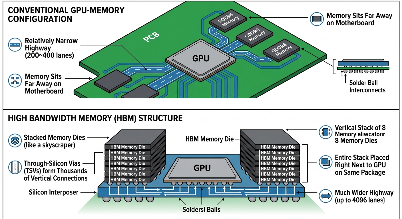 Figure. The shift from compute-bound to communication-bound AI infrastructure.
Maybe several years back, the general consensus in tech was pretty clear: software is king, hardware is just a commodity. You could make a compelling argument for that. Cloud computing was booming. You just rented compute time from AWS or Google. The real value, people said, was in the algorithms, the apps, the platforms rather than the physical machines running them.
Then ChatGPT happened.
This Substack is reader-supported. To receive new posts and support my work, consider becoming a free or paid subscriber.
Since then, everything has changed so rapidly. Then, other large language models (LLMs) followed, such as DeepSeek, Gemini, and Claude. Now, everyone realized that training and running LLMs has become one of the highest priorities, and more importantly, it is extraordinarily hungry for power, for memory, for raw compute. And all of that hunger is hardware. The smarter the AI model, the more data it needs to process, and the faster it needs to move that data around. Suddenly, hardware is not a commodity anymore but the bottleneck [1].
The market noticed immediately. NVIDIA has become the most valuable company on the planet in 2024, overtaking both Microsoft and Apple [2]. Elon Musk announced the ‘Gigafactory of Compute,’ a massive AI data center in Memphis, Tennessee, reportedly housing 100,000 NVIDIA H100 GPUs [3]. Meta, Microsoft, Google, and Amazon collectively planned to spend over $300 billion in AI infrastructure in 2025 alone [4]. These are not software bets. These are bets on hardware.
So, what exactly is the bottleneck? For AI models, the required data processing amount is significantly increasing. How does data processing work? Memories provide data to the processors (GPU and CPU) and the processors do compute. Modern GPUs show already decent computing capability [5]. But the problem is that GPUs waste a lot of time just waiting for data to arrive from other devices like memories. The bottleneck, in other words, is communication—how fast data moves between devices.
And this is only going to get worse. As AI models grow larger and AI clusters grow bigger, the distances over which data has to travel (chip-to-chip, GPU-to-GPU, rack-to-rack) keep increasing. The more GPUs you connect, the more time each one spends waiting for data. And as we will explain later, copper wire simply cannot keep up with those distances at the speeds AI requires. The emerging answer to this problem is light.
Brief Background: The Transistor Story
To understand why this matters, it helps to understand how computing got so fast in the first place. The short answer is: transistors got smaller.
Inside every processor (CPU and GPU), there are billions of tiny switches called transistors. Each transistor can be in an ‘on’ or ‘off’ state, and by switching extremely rapidly between these states, the chip performs calculations (computing essentially runs on binary language, and ‘on’ and ‘off’ represent 1 and 0). The speed at which a transistor can switch is determined by something called the RC time, which is a product of the resistance (R) and capacitance (C) of the device. Smaller transistor means shorter channel length (lower R) and smaller area (lower C), which means a smaller RC product, which means faster switching.
This is why leading semiconductor companies like Samsung, SK Hynix, TSMC, and Intel have spent decades, as well as hundreds of billions of dollars, on the relentless shrinking of transistors. From 10 micrometers in the 1970s, to 10 nanometers in 2017, to 3 nanometers today, to 2 nanometers coming soon [6]. Every generation smaller means faster, more power-efficient chips that pack more transistors into the same area. This trend, famously predicted by Gordon Moore in 1965 is known as Moore’s Law, and it drove the entire computing revolution for 60 years.
But here is the thing: shrinking transistors solves the compute problem. That is precisely why modern GPUs are so powerful; billions of tiny, fast transistors doing math in parallel. However, it does not solve the communication problem. Transistor advancement and data transmission speed are actually two separate issues. And in the AI era, communication is the primary bottleneck.
The Two Real Bottlenecks in Modern AI: Memory and Interconnects
When you train an AI model, the GPU constantly needs to fetch data from memory, do some math, send results somewhere else, fetch more data, and so on. In other words, GPUs are now spending a lot of time just waiting for data to arrive from other devices like memories. The GPU’s raw compute power is only useful if it can be fed data fast enough to stay busy. This creates two distinct bottlenecks; GPU-memory communication and device-to-device (this could be GPU-to-GPU, chip-to-chip, rack-to-rack etc.) communication. For the former, the distance data travels is much shorter, whereas for the latter, it is much longer.
Bottleneck #1: Memory Bandwidth: The HBM Revolution
The first bottleneck is between the GPU and its memory. For years, memory was simply not fast enough to keep the GPU fed. This gap is called the ‘memory wall,**’ and it has been a known problem in computer architecture since the 1990s [7].
The solution that has emerged in recent years is High Bandwidth Memory (HBM). To understand why it works, think of the data connection between a GPU and its memory as a highway. Conventional memory (like GDDR6) sits far away on the motherboard, connected to the GPU via a relatively narrow highway (200~400 copper lanes wide). However, HBM takes a completely different approach: it (1) stacks multiple memory dies vertically, like a skyscraper of chips, and (2) places that entire stack right next to the GPU on the same package. This proximity allows thousands of tiny vertical electrical connections, called Through-Silicon Vias, or TSVs, to be formed between the GPU and the memory stack, effectively building a much wider highway (up to 4096 lanes wide). More lanes means more data moving in parallel, which means higher bandwidth (bandwidth here is basically proportional to data transmission speed, so the higher the bandwidth, the more data you can move per second) [8].
The results are striking. NVIDIA’s H100 GPU integrates 80 GB of HBM3 delivering 3.35 terabytes per second (TB/s) of memory bandwidth, which is roughly 4 to 5 times more than conventional GDDR6 memory [5]. HBM has not fully eliminated the memory wall, but it has bought the industry significant breathing room.
Bottleneck #2: Interconnects: Where Copper Hits Its Limits
The second bottleneck, which is the one this article series is really about, is between chip-to-chip, device-to-device, and even rack-to-rack; a rack, if you are not familiar, is just a physical cabinet that holds servers and chips in a data center. As AI clusters grow larger, those chips need to communicate not just within a single rack, but across many racks. You need hundreds, thousands, or even tens of thousands of GPUs working together, constantly exchanging data: GPU to GPU, chip to chip, rack to rack. This is called the interconnect problem.
For decades, these interconnects were built from copper-copper traces on printed circuit boards (PCBs), copper cables between servers. And copper has served us well. But in the AI era, the required data speeds have outpaced what copper can comfortably handle. Why?
Problem 1: Copper Is Not Suitable for High-Speed, Long-Distance Communication
The fundamental issue is a phenomenon called the skin effect. At high frequencies (if you are not familiar with the term “frequency”, just think it as the speed of the signal), electrical current does not travel through the entire cross-section of a copper wire, but it increasingly concentrates near the surface (the ‘skin’). As frequency increases, the effective conducting area shrinks, resistance rises, and signal power is absorbed as heat. This effect gets dramatically worse at higher frequencies [9].
To put numbers on it: at a frequency of 56 GHz, a standard copper trace loses around 10% per cm (0.5 dB of signal per centimeter). Chip-to-chip connections across a server board span 20 to 50 centimeters (only 10% to 0.3% left); rack-to-rack connections span 1 to 5 meters or more (0% signal transmitted). By the time a signal travels even a few tens of centimeters at these frequencies, it has weakened to the point where you need expensive, power-hungry amplification and equalization circuitry just to recover it [10].
Problem 2: Previous Computing Did Not Require Long-Distance, High-Frequency Communication
Here is the thing: this was not always a problem. Conventional computing was mostly about fast communication within a single motherboard, between a CPU, GPU, and memory sitting centimeters apart. Copper was perfectly fine for that. The distances were short, the number of chips talking to each other was small, and the required frequencies were manageable.
AI changed all of this. Training a large language model (LLM) would require hundreds of thousands of GPUs spread across many servers and racks, all constantly exchanging data. The distances are longer, the number of communicating chips is vastly larger, and the required speeds are much higher. Copper simply was not designed for this regime.
And there is one more problem: heat. All that signal energy absorbed by the copper does not disappear but becomes heat. Modern data centers already consume gigawatts of power, a significant portion of which goes into just moving data over copper rather than computing with it. A state-of-the-art 800 G pluggable optical transceiver consumes about 15 to 17 watts per port. The co-packaged optical solutions we will discuss later in this series bring that down to roughly 4 to 5 watts per port, a roughly 70% reduction [11]. Across tens of thousands of ports in a large AI cluster, that difference is measured in megawatts.
So, copper has essentially hit its limits for the demands of modern AI infrastructure. The industry needs something fundamentally different, which is “light”.
Enter Optical Interconnects: Why Light Is the Answer
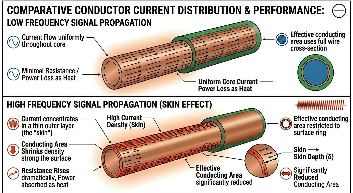 Figure. Photons: no charge, no mutual interaction, near-zero propagation loss — the answer to copper’s limits.
So, if copper is struggling, what is the alternative? The answer is the industry is converging on light, optical interconnects that transmit data as pulses of light rather than electrical current.
Why light? Here is the intuition: electrons are physical particles. When they flow through a conductor, they collide with atoms in the lattice, losing energy as heat (that is resistance). At high frequencies, they pile up near the surface (that is the skin effect). They also interact electromagnetically with nearby electrons in adjacent wires (that is cross-talk). All of these effects get worse as you push for higher speeds.
Photons, the particles of light, behave very differently. They do not carry electrical charge, so they do not interact with each other or with the atoms of the waveguide they travel through (assuming the material is transparent). A photon traveling through a well-engineered optical waveguide or fiber experiences essentially zero resistive loss, generates no heat from propagation, and does not cross-talk with neighboring optical signals [12]. These properties hold true whether you are operating at 1 GHz or 1,000 GHz because light does not have a ‘skin effect’.
And here is perhaps the most powerful advantage: you can carry multiple completely independent data streams on different wavelengths (colors) of light, all traveling through the same physical waveguide simultaneously. This is called Wavelength Division Multiplexing (WDM), and it is how a single optical fiber can carry a terabit per second of data. No copper wire can do that.
Optical fiber has been the backbone of the global internet and telecommunications network for decades for exactly these reasons: low loss (as little as 0.17 dB per kilometer [13]), high bandwidth, and immunity to electromagnetic interference. What has changed recently is that photonic technology is now being miniaturized onto semiconductor chips (which is called Photonic Integrated Circuits, PICs) making it practical to use optical interconnects not just between cities, but between chips on the same circuit board or even within the same package.
That is what this series is about: the technology, the science, and the industry behind bringing light onto the chip, and why it may be the most important hardware development of the AI era.
A Map of What’s Ahead
Before diving in, here is a quick preview of the main components I would like to discuss in this series, the building blocks of a Photonic Integrated Circuit (PIC):
High-speed Modulators: The component that takes a laser beam and encodes digital data onto it. We will look at several different technologies, silicon, lithium niobate, barium titanate, organic hybrids, indium phosphide, and polymer, each with different speed, voltage, and integration trade-offs.
Lasers: Silicon cannot generate light on its own (it has the wrong electronic structure for that). Getting a laser source integrated on a silicon chip is one of the central challenges of the field, and several clever solutions have emerged.
Phase Shifters: Components that precisely control the phase of light.
Photodetectors: The component at the receiving end, converting pulses of light back into electrical signals.
Fiber-to-Chip Coupling: How do you get light on and off a chip whose waveguides are only a few hundred nanometers wide? A surprisingly tricky engineering challenge.
Optical Transceivers and Co-Packaged Optics (CPO): The full system: how all these components come together into the products actually shipping in data centers today, from 400 G pluggable modules to the co-packaged optics (CPO) that will define the next generation of AI networking hardware.
Along the way, we will connect the technology to the real companies building it: Intel, Marvell, Broadcom, Cisco, Coherent, Ayar Labs, Lightmatter, HyperLight, TSMC, GlobalFoundries, and a wave of startups you have probably not heard of yet, but should.
Let’s start with the foundations.
References
[1] J. Dean, ‘A Golden Decade of Deep Learning: Computing Systems and Applications,’ Daedalus 151(2), 58-74 (2022). DOI: 10.1162/daed_a_01900
[2] CNBC (June 18, 2024). ‘Nvidia passes Microsoft as world’s most valuable public company.’ https://www.cnbc.com/2024/06/18/nvidia-passes-microsoft-in-market-cap-is-most-valuable-public-company.html. Also: CNBC (November 5, 2024). ‘Nvidia passes Apple as world’s most valuable company.’ https://www.cnbc.com/2024/11/05/nvidia-passes-apple-as-worlds-most-valuable-company-.html
[3] xAI Colossus supercomputer, Memphis, Tennessee. Initial cluster: 100,000 NVIDIA H100 GPUs, built in 122 days. Sources: Supermicro case study (https://www.supermicro.com/CaseStudies/Success_Story_xAI_Colossus_Cluster.pdf); Wikipedia: Colossus (supercomputer) (https://en.wikipedia.org/wiki/Colossus_(supercomputer))
[4] CNBC (February 8, 2025). ‘Tech megacaps plan to spend more than $300 billion in 2025 to win in AI.’ Breakdown: Amazon ~$, Microsoft ~$, Alphabet ~$, Meta ~$. https://www.cnbc.com/2025/02/08/tech-megacaps-to-spend-more-than-300-billion-in-2025-to-win-in-ai.html
[5] NVIDIA H100 Tensor Core GPU Datasheet (2023). https://resources.nvidia.com/en-us-tensor-core/nvidia-tensor-core-gpu-datasheet
[6] Transistor node history: Intel 4004 (1971, 10 um); TSMC 10 nm volume production 2017; TSMC N3 (3 nm) 2022; TSMC N2 (2 nm) targeted 2025. Sources: Wikipedia – 10 nm process (https://en.wikipedia.org/wiki/10_nm_process); TSMC N2 (https://en.wikipedia.org/wiki/TSMC_N2)
[7] W. Wulf and S. McKee, ‘Hitting the Memory Wall: Implications of the Obvious,’ ACM SIGARCH Computer Architecture News 23(1), 20-24 (1995). DOI: 10.1145/216585.216588
[8] Samsung Electronics HBM3 Technical Overview (2022). https://semiconductor.samsung.com/us/consumer-storage/hbm/. HBM interface width: 1024-bit per die (4096-bit for 4-die stack) vs. GDDR6 at 256-384 bit. Through-Silicon Via (TSV) technology enables this wide bus.
[9] S. Ramo, J. R. Whinnery, T. Van Duzer, Fields and Waves in Communication Electronics, 3rd ed. (Wiley, 1994). Chapter 5: Skin effect and transmission line losses.
[10] PCB copper trace attenuation at 56 GHz: approximately 0.5 dB/cm on standard FR4 laminate. Source: Signal Integrity Journal, ‘Next-Generation PCB Loss Analysis.’ https://www.signalintegrityjournal.com/articles/3159-next-generation-pcb-loss-analysis. Also: IEEE 802.3ck Task Force (2021), channel loss modeling at 112 Gbps PAM4.
[11] 800G pluggable optical transceiver: ~15-17 W per port. Co-packaged optics (CPO): ~4-5 W per port (~70% reduction). Sources: SemiAnalysis CPO newsletter (https://newsletter.semianalysis.com/p/co-packaged-optics-cpo-book-scaling); APNIC Blog (May 2025), ‘Co-packaged optics: a deep dive’ (https://blog.apnic.net/2025/05/07/co-packaged-optics-a-deep-dive/)
[12] B. E. A. Saleh and M. C. Teich, Fundamentals of Photonics, 3rd ed. (Wiley, 2019). Chapter 9: Fiber Optics.
[13] Corning SMF-28 Ultra Optical Fiber Product Information Sheet (2022). Attenuation: 0.17 dB/km at 1550 nm. https://www.corning.com/media/worldwide/coc/documents/Fiber/SMF-28%20Ultra.pdf
This Substack is reader-supported. To receive new posts and support my work, consider becoming a free or paid subscriber.
第二部分:解析(深度解读)
核心论点摘要
光子学博士 PhotonEra 用一篇面向大众的系列开篇,论证了一个被「算力叙事」遮蔽的事实:AI 时代的真正瓶颈不是算力,而是「通信」——数据在芯片、GPU、机架之间移动的速度。
推理链:
- ChatGPT 之后,市场才猛然意识到硬件才是瓶颈(NVIDIA 2024 登顶、四大云厂 2025 年合计砸 $3000 亿+);
- GPU 大量时间花在「等数据」上——瓶颈是 communication;
- 晶体管缩放(摩尔定律)解决了 compute,但没解决 communication,二者是两回事;
- 两大瓶颈:GPU-内存通信(内存墙) 与 设备间互连(互连问题);
- 内存墙靠 HBM(垂直堆叠 + TSV 宽总线,H100 达 3.35 TB/s)缓解;
- 互连瓶颈靠光解决:铜在 56GHz 有趋肤效应(0.5 dB/cm 损耗)、发热、串扰,且机架级距离信号归零;
- 光子(PIC)无电荷、不互作用、近零传播损耗、可 WDM——天然胜出;
- 系列后续将拆解 PIC 核心器件(调制器/激光器/移相器/探测器/光纤耦合/CPO)与产业链公司(Intel、Marvell、Broadcom、Cisco、Coherent、Ayar Labs、Lightmatter、HyperLight、TSMC、GlobalFoundries 等)。
关键概念解读
- 内存墙(Memory Wall):自 1990s 起就存在的架构难题——内存速度跟不上计算。HBM 通过「垂直堆叠 + TSV 宽总线」把 GPU-内存 highway 从 200–400 铜 lane 拓宽到 4096 lane,带宽约 4–5× GDDR6。
- 趋肤效应(Skin Effect):高频下电流挤到导体表面,有效截面积缩小、电阻上升、能量变热。56GHz 时标准铜走线 ~0.5 dB/cm 损耗;板级 20–50 cm 后只剩 10%–0.3% 信号,机架级(1–5 m)基本归零。
- 互连问题(Interconnect Problem):AI 集群要把成千上万 GPU 跨芯片/跨机架连起来,铜的物理极限(距离 + 频率 + 热)在此 regime 下失效。
- 光子集成电路(PIC, Photonic Integrated Circuit):把光器件微缩到半导体芯片上,使光互连从「城市间」走向「同一板卡甚至同一封装内」。
- WDM(波分复用):同一波导不同波长同时传多路独立数据,单纤可达 1 Tbps——铜做不到。
- 光收发器 vs CPO:800G 可插拔 ~15–17 W/端口;CPO ~4–5 W/端口(约降 70%),数万端口累计差值为兆瓦级。
技术拐点与产业含义
- 「算力 vs 通信」是两件事:文章最有价值的纠正——晶体管缩放只解决 compute,通信瓶颈需另寻解(光)。这正解释了为什么 CPO / 光互连成为 2025–2026 最热硬件主题。
- 铜的极限是定量的:56GHz 单板 0.5 dB/cm,机架级信号归零 → 光填铜让出的地盘是刚需,不是噱头。
- 热是隐形杀手:铜吸收的信号能变热,数据中心 GW 级功耗里有可观一部分花在「搬数据」而非「算数据」;CPO 降功耗约 70%,在万端口集群里是 MW 级差异。
- PIC 器件链即投资地图:调制器(硅 / 铌酸锂 / 钛酸钡 / 有机杂化 / InP / 聚合物)、激光器(硅不能发光,是核心挑战)、移相器、探测器、光纤-芯片耦合、CPO 系统——每一环都对应一批公司(Lightmatter、Ayar Labs、HyperLight 等是代表)。
与本站其他文章的连接
- 本篇是 CPO / 光互连系列在「为什么需要光」层面的总纲:本站的 Pushing the Speed Limit:224/448Gbps 时代的 SerDes 收发器架构拆解 讲电侧 SerDes 如何撞墙,SerDes 技术全景(上篇) 讲并串转换与 PAM4,本篇则从「铜的物理极限 + 光子优势」给出必须走向光的底层理由。
- 光侧器件供货方与标的见 Sivers Semiconductors:一只被市场忽视的 $130M 市值 CPO / LiDAR / SATCOM 标的(InP DFB 激光阵列)与本站 CPO 专题(CPO Fully Dissected、CPO Biggest Bottleneck: High Volume Testing 等)。
风险提示
- 本文为科普译介,不构成投资建议;所涉公司(NVIDIA、Intel、Marvell、Broadcom、Cisco、Coherent、Ayar Labs、Lightmatter、TSMC、GlobalFoundries 等)仅作技术产业链梳理,未做估值判断。
- 数据时效:原文数据截至 2026-04,部分产能、功耗与产品节点(如 TSMC N2 目标 2025)可能已有更新,请以最新公开披露为准。
- 技术路线风险:PIC 各器件(尤其硅上集成激光器、光纤-芯片耦合良率)仍有工程与成本挑战;CPO 渗透率与时间表受良率、生态与标准牵制。
- 英文原文图表版权归原作者 PhotonEra 及所引来源(CNBC、NVIDIA、Corning、SemiAnalysis、APNIC 等)各自所有,引用已标注来源。