MicroLED 与激光器之争:线宽如何锁死数据中心光互连的速率上限
Vikram Sekar 从第一性原理拆解 MicroLED 与 DFB 激光器之争:线宽经色散决定脉冲展宽、进而锁死单通道速率上限。DFB 线宽 0.001nm 量级而 MicroLED 达 40nm——差 4 到 5 个数量级,故 MicroLED 需 400 条通道(20×20×2Gbps)才能凑出 800G,而 DFB EML 只需 4 条。作者的算例我重新验算过:第二例存在 ps/ns 单位口径不一致,偏保守约三个数量级。含英文原文完整转载(8 张配图)与中文深度解读。
来源:Viks Newsletter(Substack,半导体行业分析)— MicroLEDs vs. Lasers: The Linewidth Tradeoff 副标题:Why spectral purity defines the speed limits of datacenter optics 作者:Vikram Sekar(@vikramskr) 原文链接:https://www.viksnewsletter.com/p/microleds-vs-lasers-the-linewidth-tradeoff | 原文发布日:2026-04-07 | 本站发布:2026-09-21 付费状态:全文公开(
audience = everyone),无付费墙,第一部分为完整转载 本页内容:第一部分为英文原文完整转载(含全部 8 张配图,仅调整排版层级与剔除站点订阅推广段);第二部分为独立撰写的中文深度解读,其中带质疑与核算的判断属解读者观点,不代表原作者立场。
第一部分:正文(Original Article / 英文原文)
There has been considerable chatter about Lumentum’s lasers and their narrow linewidth, contrasted with questions about the viability of microLEDs in datacenters. I’ve been meaning to write about microLEDs for quite a while; we’ll cover some general aspects here. Since MicroLEDs are a big topic, this is best handled as a sequence of posts that build up the whole picture over time. We will make constant comparisons to lasers since it is the incumbent optical technology. Feel free to ask follow up questions in the comments at any time - it will help guide future posts.
A useful starting point to understand the lasers versus LEDs debate is to ask what linewidth is, why it matters, and how lasers and LEDs broadly compare. Let’s first describe the technology landscape.
Lumentum, Coherent, and DFB Lasers
Distributed Feedback (DFB) lasers often made from Indium Phosphide (InP) are known for their narrow linewidth, where Lumentum holds dominance in 200G/lane electro-absorption modulated lasers (EMLs). Their moat comes both from having a great laser source and a co-optimized modulator that encodes high-speed electrical signals into light. The performance gap in EMLs is seemingly wide enough (specs not published widely) that their competitor, Coherent, actually buys these EMLs from them. This puts Lumentum in the driver’s seat for EMLs in the 1.6T optical era involving pluggable transceivers.
A DFB laser for co-packaged optics (CPO) is a different beast and is a space where Lumentum has serious competition. CPO requires a constant source of light (called continuous-wave or CW) because the modulation is handled by the silicon photonics chip using a ring or Mach-Zehnder modulator. Here, a constant output power of 300-400mW at elevated temperatures of 50-70°C is the key differentiator. This level of output power is needed because the light source is outside the rack, and connected to the SiPho chip via a long polarization maintaining optical fiber. We’ve discussed this earlier.
Laser Linewidth, RIN, and Power
Lumentum’s ELS laser for CPO has an advertised output power of 350 mW at 50°C, a line width of <500 kHz, for a 1311 nm laser. Coherent’s equivalent laser has a reported output power of 400mW at 50°C and a linewidth of <200 kHz. Linewidth is a measure of how pure the light source is, and is quantified by the Full-Width at Half-Maximum (FWHM). Take the maximum laser power, cut it by half and measure the spreading of the laser frequency/wavelength. The smaller this number, the more pure the laser output on the spectrum.
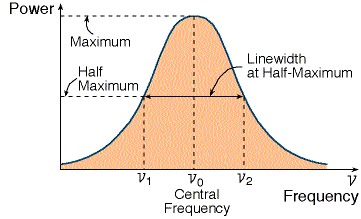
Source: Rami Arieli, “ The Laser Adventure ”
Anything under 1 MHz in linewidth is exceptionally pure light, really. A 1311nm laser translates to about 230 THz in free space which is really narrow compared to the center frequency. The deviation in wavelength is so small that laser engineers prefer frequency units to represent this. This is the magic of DFB lasers.
Lasers from both companies have a Relative Intensity Noise (RIN) of -145 dB or thereabouts. RIN is a measure of how stable the output power is. Think of a bad laser with high RIN as flickering too much. Lumentum is not much better in RIN; the frequently cited -156 dB RIN for Lumentum is a hero number from a CLEO 2022 paper. Their production RIN is in the same ballpark as Coherent. Thus, while Lumentum has a clear advantage in EMLs for pluggables, the race to CPO lasers is highly contested (there are other players but their laser specs are not publicized).
Regardless of lasers for pluggables or CPO, the key takeaway is that DFB lasers with their narrow linewidth are perfectly suited for optical communication, and have been the mainstay for long haul links. They allow encoding of fast data signals and have long distance reach. Here is the critical question: is DFB laser the right choice of technology for short-to-medium distance optical links in a datacenter?
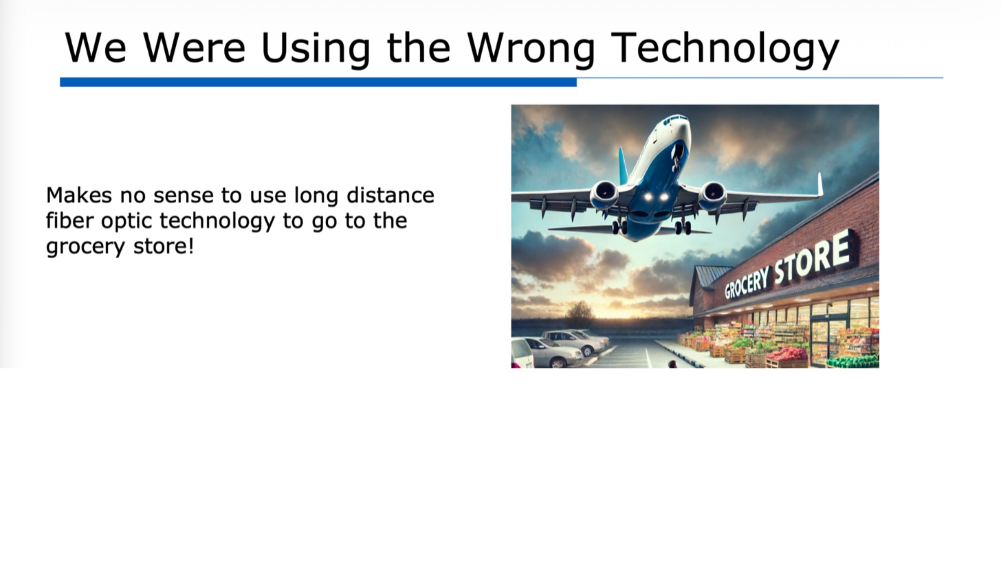
Avicena thinks DFBs are like using an airplane to get to the grocery store. Source: ISSCC 2025 Forum 1.
The Case for MicroLEDs: Benefits and Challenges
There has been a slew of activity around the use of Micro Light Emitting Diodes (LEDs) for data transmission. Credo moved to acquire Hyperlume last year, Microsoft published results from Mosaic, and Marvell most recently is collaborating with Mojo Vision on microLEDs. We would be remiss if we did not mention Avicena, who has been pioneering MicroLEDs for AI interconnects for a long time.
MicroLEDs are just really small versions (10-50 microns in size) of your regular lightbulbs, and are built with Gallium Nitride (GaN) to emit blue light. Just like you don’t get a laser light show every time you walk in your room and turn the light on, microLEDs do not emit a narrow pencil beam of light like lasers. They instead produce light in a wide angle and need to be focused with a microlens. The light is not spectrally pure like lasers either. Blue GaN microLEDs have a wavelength of about 450nm, and linewidths of 10-15nm. Compared to lasers, this is terrible linewidth because it accounts for about 3% around the center wavelength.
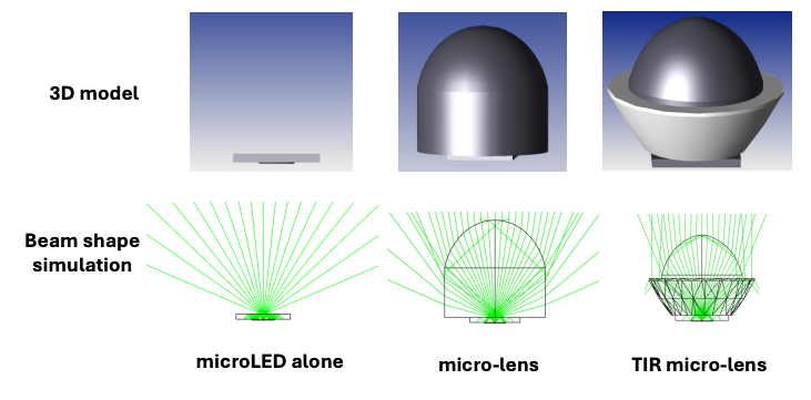
Source: Microsoft
The poor linewidth in comparison to lasers imposes restrictions on data rate that a microLED optical link can support. The solution around this is to use an array of microLEDs in a “wide-but-slow” approach – just like each data lane in high bandwidth memory (HBM) is slower than what is possible in GDDR, but the overall throughput is higher. There are a few additional benefits of using microLEDs:
- Lower power than DFB laser optics (caveat to follow), but better reach than copper (can possibly do >10m at Tbps aggregate speeds)
- Better reliability than lasers because LEDs are structurally simpler, and relatively temperature insensitive. A wide-but-slow approach means that there could be redundant lanes for failover.
- Linear path to scaling to higher speeds: increase per-lane speed (harder) or increase number of lanes (easier).
While microLED cables would work directly with existing pluggable infrastructure, there are two important requirements that makes things more complex:
Focusing optics
The broad angle emission from a microLED needs to be focussed with microlenses in order to couple them into an array of optical fibers that carry multiple parallel lanes of data. In reality, this is not difficult because microlenses are also implemented as an array that fits directly over the microLED array. DFB laser sources have specialized optics to couple light into fibers too.
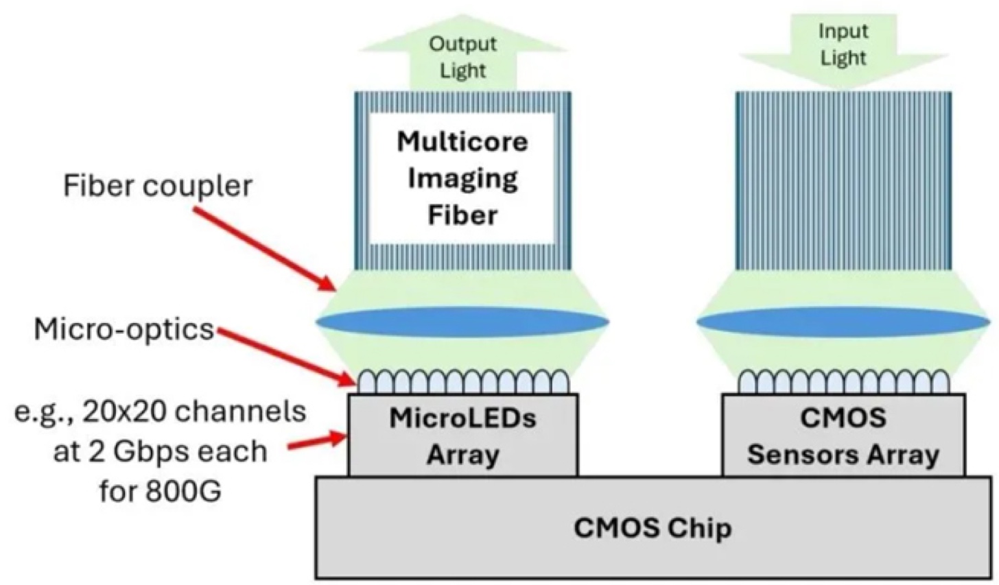
Source: Lanaotek
Electrical Gearboxing
You need an “electrical gearboxing” function that converts the 112G/224G narrow-but-fast SerDes lanes of the host processor into a 20 x 20 microLED array that carries slow-but-wide signals at lower data rates. This chip is implemented as a CMOS ASIC that handles the electrical gearboxing. For example, the Avicena LightBundle™ evaluation kit launched at OFC 2026 uses a specialized 16nm finFET CMOS ASIC. The only way a gearbox chip can be avoided is to design the host processor with a UCIe interface that natively implements a wide-but-slow approach (like a custom base-die used in HBM).
Microsoft’s paper on microLEDs shows that the gearbox functionality only consumes a small portion of the power (0.4W) it would otherwise take with an optical connection that requires DSP/CDR/FEC (3.5W). The argument in the paper is that it is a simple gearboxing function, and thus less power hungry. If per-lane speeds increase in future generations of microLED interconnect, then CDR/FEC functions will be required and power usage will increase, closing the power efficiency gap between lasers and microLEDs.

Source: Microsoft Mosaic
Why linewidth matters for data rates
Let’s address why microLEDs are only capable of 2-4 Gbps data rates today in pre-production, while DFB EMLs can support 200 Gbps or more.
The fundamental concept that underlies this limitation is chromatic dispersion in an optical fiber. When an optic signal travels through a fiber, different wavelengths travel at different speeds due to the wavelength-dependent refractive index of glass in the fiber. The resulting pulse exiting the fiber spreads out in time because different wavelengths arrive at different times.
This spreading determines the maximum speed of data transmission that is possible because once neighboring pulses start to overlap, it is hard to tell them apart and detection errors start to occur.
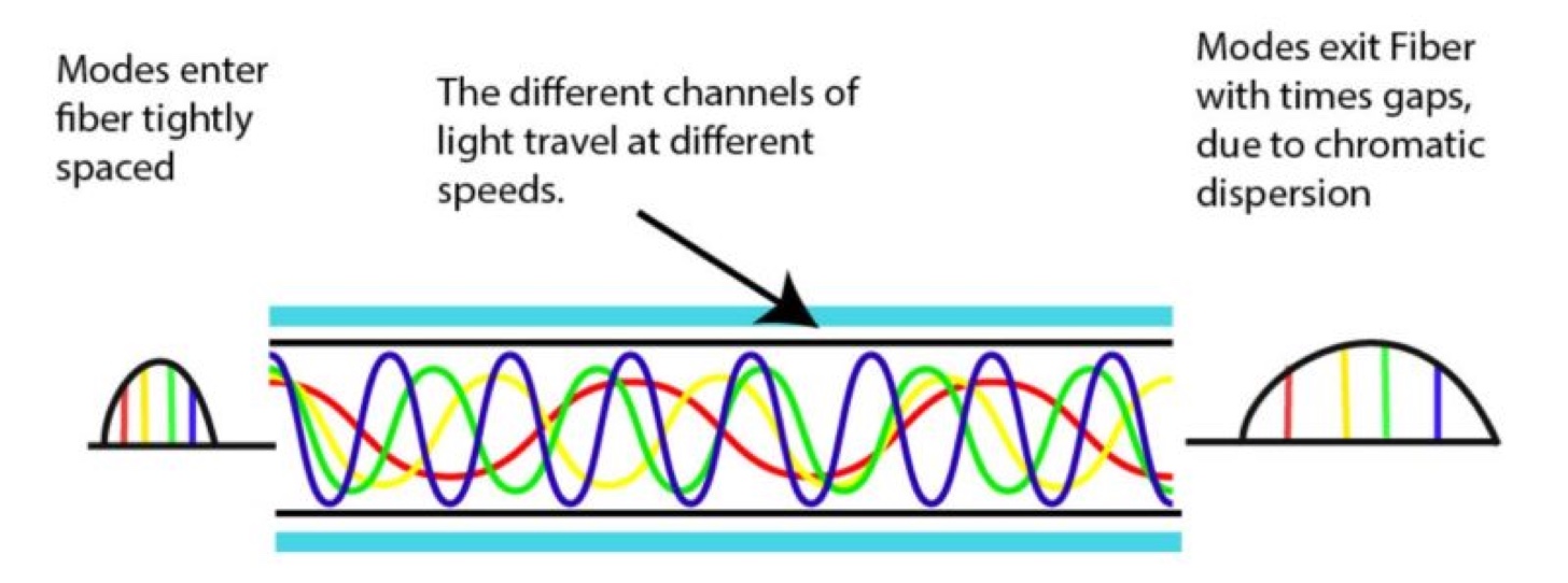
Source: Mohamed Abolfotouh on Linkedin
The broadening of a pulse by a time dT (ps) in an optical fiber can be calculated as
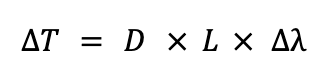
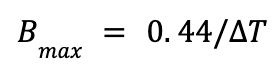
Where D is the dispersion coefficient in ps/(nm·km), L is the link length in kilometers, and is the linewidth of the light source. Assuming Gaussian pulses are being transmitted as bits, the data rate Bmax is:
Let’s try out some numbers here.
With a microLED
A standard legacy multimode optical fiber (such as OM3 or OM4) operating at 850 nm exhibits a material dispersion parameter of approximately 100 ps/nm/km.n For an 850 nm microLED with a spectral linewidth of 40 nm (4.7% of center wavelength), operating over a link length of 0.010 km (10 meters), the temporal pulse spread is calculated as: 100×0.01×40, or 40ps. Maximum data rate supported = 0.44/40ps = 11 Gbps/lane. These speeds have been demonstrated in research papers with microLEDs, but production numbers are slower at 2-4 Gbps/lane.
With a DFB laser
Let us assume the same wavelength, and same link distance, but a linewidth of 0.001nm. The temporal pulse spread is: 100×0.01×0.001 = 0.001ps. Maximum data rate supported = 0.44/0.001 = 440 Gbps/lane.
This demonstrates why linewidth makes a big difference in how much data rate is possible with a given type of light source in an optical communication system.
There is a lot more to discuss about microLEDs before we can declare microLEDs fit/unfit for datacenter needs: coupling efficiency into fibers, beam shapes, reliability assessments, and the overall supplier/customer landscape that is still rapidly evolving.
Industry sources tell me that hyperscalers are open to exploring microLEDs for future interconnect needs, but the microLED industry for datacenter interconnects is still young. An additional aspect worth exploring is how VCSELs compare as an alternative to microLEDs – something that Lumentum is actively exploring with 1060nm VCSELs. So many future post options!
第二部分:中文深度解读
以下为独立撰写的中文解读,非原文翻译。文中带有质疑、核算与边界的判断属于解读者观点,不代表原作者立场。原文所有定量结论我都按文中给出的公式重新验算过,验算结果与差异在第四节与第六节逐条列出。
一、这篇文章在讲什么
一句话:这是一篇关于「光源光谱纯度如何决定数据中心光互连速率上限」的第一性原理拆解,也是一组「MicroLED vs 激光器」系列文章的开篇。
作者 Vikram Sekar(半导体行业分析 newsletter Viks Newsletter)抛出的对立面很具体:一边是 Lumentum 的 DFB 激光器及其引以为傲的窄线宽,另一边是被反复质疑「在数据中心到底能不能用」的 MicroLED。他给出的答案不是站队,而是把问题退回物理层——先搞清楚线宽是什么、为什么它决定速率,再谈两种技术各自的系统级代价。
这篇文章的定位需要先摆清楚:它不是一篇「MicroLED 判决书」,作者自己明确说了「MicroLED 是个大题目,这应该作为一系列文章来处理」。所以全文只完成了三件事:① 建立线宽的语言;② 给出激光器阵营的现状(Lumentum / Coherent 的规格对照);③ 用色散模型给出速率上限的量化算例。真正决定 MicroLED 成败的那些工程问题——耦合效率、光束形状、可靠性评估、供应链格局——被作者列出来但留待后续。
二、作者的坐标系:一切从「线宽」这一个参数出发
理解全文只需抓住一条因果链:
1
光源线宽 Δλ  ──>  光纤中的色散  ──>  脉冲在时间上展宽 ΔT  ──>  相邻比特重叠  ──>  误码  ──>  数据率上限
这条链上每一环都有明确公式,作者把最关键的两个直接贴成了图片:
\[\Delta T = D \times L \times \Delta\lambda\] \[B_{max} = 0.44 / \Delta T\]其中 D 是色散系数(ps/nm/km),L 是链路长度(km),Δλ 是光源线宽(nm);0.44 是高斯脉冲的时间-带宽积系数。注意这两个公式是理解全文的分水岭:它们说明数据率上限与线宽成反比,而线宽恰恰是激光器对 MicroLED 碾压得最彻底的一个参数。
于是作者的论述重心落在了一个反直觉的位置上:MicroLED 在线宽这一项上必输,且不是输一点,是输好几个数量级。那么它凭什么还有机会? 全文后半段就是在回答这个「凭什么」。
三、两位主角的规格底牌
作者给出的对照非常干净:
| 参数 | Lumentum ELS(CPO 用) | Coherent 同类产品 |
|---|---|---|
| 输出功率 | 350 mW @ 50°C | 400 mW @ 50°C |
| 线宽 | < 500 kHz | < 200 kHz |
| 中心波长 | 1311 nm | 未明示(同类) |
| RIN | ≈ −145 dB | ≈ −145 dB(同级) |
这里有三处值得单独拎出来的判断。
第一,Lumentum 最强的位置不在 CPO,在可插拔。 作者点明了:Lumentum 在 200G/lane 的 EML(电吸收调制激光器)上居于支配地位,护城河来自「好的激光源 + 共同优化的调制器」的组合,以至于竞争对手 Coherent 反过来要买它的 EML。这个格局在 1.6T 可插拔时代仍然成立。
第二,CPO 用的 DFB 是「另一种野兽」。 CPO 需要的是连续波(CW)光源,因为调制由硅光芯片上的环形或 MZ 调制器完成。此时关键指标变成了「50–70°C 高温下 300–400 mW 的恒定输出功率」——因为光源在机架外,要经长距离保偏光纤连到硅光芯片。注意这句话的深层含义:CPO 场景下,激光器被推出了机架,线宽的重要性其实让位给了功率与温稳。
第三,作者主动戳破了一个行业叙事。 常被引用的 Lumentum「−156 dB RIN」被作者直接定性为「来自 CLEO 2022 论文的 hero number」,其量产 RIN 与 Coherent 在同一水平。这句「hero number」是全文最值得记住的用词——它代表了一种读行业规格书的正确姿态:论文里的最优值 ≠ 量产规格,厂商新闻稿 ≠ 可依赖的对比基准。
结论:在可插拔 EML 上 Lumentum 优势明确;在 CPO 激光器上则是一场高度胶着的竞争(且还有其他玩家,只是规格未公开)。
四、MicroLED 的账:从物理劣势到工程应对
4.1 物理上的天然劣势
MicroLED 本质是「极小的(10–50 μm)普通灯泡」,用 GaN 发蓝光。作者用了一个很妙的类比:开灯不会出现激光秀——MicroLED 不像激光那样发出细窄的笔形光束,而是大角度发散(需微透镜聚焦),光谱也不纯。蓝光 GaN MicroLED 约 450 nm,线宽 10–15 nm,即中心波长的约 3%;而激光器可以做到 < 1 MHz(相对线宽小到用频率而非波长表述更合适)。
这就是那个「宽而慢」策略的物理起点: 单通道速率被线宽锁死,那就用通道数换总带宽。作者用 HBM 作类比——HBM 每条 lane 都比 GDDR 慢,但总吞吐更高。这个类比是全文最有力的一个,因为它把一个「缺点」重新框定为一种已被产业验证过的成熟范式。
4.2 三项宣称的收益(含一处作者自己埋的 caveat)
- 功耗低于 DFB 激光方案(作者明确加了「caveat to follow」——见下文);
- 可靠性优于激光器:LED 结构更简单、对温度相对不敏感,且「宽而慢」架构天然允许冗余 lane 做失效切换;
- 向更高速率的路径是线性的:提升单 lane 速率(难)或增加 lane 数(易)。
第 1 条的 caveat 作者在后文兑现了,而且兑现得相当诚实:Microsoft 的 Mosaic 论文显示 gearbox 功能仅耗 0.4 W,而需要 DSP/CDR/FEC 的光连接要 3.5 W——但这个优势是有条件的:如果未来 MicroLED 的单 lane 速率提升,CDR/FEC 功能将变得必要,功耗优势随之收窄,最终会闭合。
4.3 两项绕不开的复杂度
聚焦光学(Focusing optics):microLED 的大角度发散需要微透镜阵列耦合进多芯光纤。作者认为这不算难,因为微透镜同样可以做成阵列、直接覆盖在 microLED 阵列之上。
原文随文的架构图给出了整篇最有价值的工程数字:20×20 通道阵列、每通道 2 Gbps、合计 800G。这个数字值得停下来算一笔账——800G 用单通道 200G 的 DFB EML 只需 4 条 lane;用 MicroLED 则需要 400 条。通道数差 100 倍,单通道速率仅为对方的 1%。 这就是「wide-but-slow」的量化代价,也是它所有优点(冗余、温稳、无 DSP)的来源。
电学 gearboxing:需要一个 CMOS ASIC,把主机处理器的 112G/224G 窄而快 SerDes lane 转换成 20×20 的慢而宽驱动信号。Avicena 在 OFC 2026 发布的 LightBundle™ 评估套件用的是一颗专用 16 nm FinFET CMOS ASIC。作者指出,唯一能省掉 gearbox 芯片的办法,是让主处理器原生实现 UCIe 接口下的宽而慢方案(如同 HBM 用的 custom base-die)——这实际上是在要求整个计算架构围绕 MicroLED 的物理特性重做。
这一节隐含了一个作者没有明说、但值得点出的结构性判断: MicroLED 的「低成本」只体现在光域,它的电域复杂度被搬到了 gearbox ASIC 与主机接口上。所谓「省电 3–4 倍」(见第六节的功耗账),是这两笔账相抵之后的结果,而不是光源本身的功劳。
五、我按文中公式重新算了一遍
作者给出的算例是全文的核心论证,我用文中两个公式严格复核(并在第六节指出一处单位口径问题)。
公式复核(D = 100 ps/nm/km,L = 0.010 km = 10 m):
| 光源 | 线宽 Δλ | ΔT = D·L·Δλ | 作者给出的 Bmax | 我的复核 |
|---|---|---|---|---|
| MicroLED(850 nm,多模光纤) | 40 nm | 40 ps | 11 Gbps/lane | ✅ 一致 |
| DFB(激光器) | 0.001 nm | 0.001 ps | 440 Gbps/lane | ⚠️ 单位口径存疑,见第六节 |
作者随即给出一个很重要的现实校正:11 Gbps/lane 是研究论文里已演示的水平,量产的 MicroLED 目前只有 2–4 Gbps/lane。 这与架构图里「2 Gbps/通道」的工程取值互相印证,也与「DFB EML 可支持 200 Gbps 以上」形成对照。
六、我的评述:三处需要指出来的问题
6.1 算例的单位口径不一致(本次复核的主要发现)
按文中给出的公式 Bmax = 0.44/ΔT 严格代单位复核:
- 第一例:ΔT = 40 ps = 0.04 ns → 0.44/0.04 = 11 Gbps ✅ 与作者一致;
- 第二例:ΔT = 0.001 ps = 1×10⁻⁶ ns → 0.44/1×10⁻⁶ = 4.4×10⁵ Gbps,而作者写的是 440 Gbps。
也就是说,作者在第二例中把 ΔT 的 ps 数值直接当作 ns 代入(0.44/0.001 = 440),与第一例的处理相差三个数量级。
必须同时说明两点,否则这个发现会被误读:
- 该差异的方向是保守的,它低估了 DFB 的能力,因此不改变结论方向——色散限制下 DFB 与 MicroLED 的差距比文中呈现的更大,而不是更小;
- 当 Bmax 算到 10⁵ Gbps 量级时,这个模型本身已经失去工程意义。10 米链路的真实瓶颈早已不是色散,而是调制器带宽、驱动电路与封装寄生。作者写 440 Gbps 可能正是出于「让数字保持在有意义区间」的直觉——但严格来说,算例里混用单位是需要修正的。
这个瑕疵的价值在于它揭示了一件事:色散模型只对 MicroLED 一侧有约束力。 对激光器而言,它是「根本不构成限制」的那一类约束;对 MicroLED 而言,它是「决定生死」的那一类约束。用同一个公式同时论证两边,容易让人误以为这是一场同量级的比较,而实际上它是「约束存在 vs 约束不存在」的区别。
6.2 正文的 MicroLED 参数与算例的参数不是同一组
这里有一处容易被忽略的口径切换:
| 位置 | 波长 | 线宽 | 相对线宽 |
|---|---|---|---|
| 正文描述(blue GaN) | 450 nm | 10–15 nm | 约 2.2% – 3.3% |
| 算例实际取值 | 850 nm | 40 nm | 约 4.7% |
算例用的是 850 nm + 多模光纤(OM3/OM4)这一 legacy 场景,而非正文所述的 450 nm 蓝光 GaN。 这样处理在技术上自洽——100 ps/nm/km 正是 850 nm 多模光纤的典型材料色散系数,而 450 nm 下的色散系数完全不同,不能直接套用。但读者需要意识到:算例给出的是「多模光纤 + 850 nm」这一路线的结论,而不是「MicroLED 这个器件」的普遍结论。 把 11 Gbps 当作 MicroLED 的天花板是过度的推论。
6.3 真正的争论不在线宽,而在「谁承担复杂度」
作者的论证很容易被读成「MicroLED 因为线宽差所以速度慢」,但把全文摊开看,实际的结构是这样的:
| 维度 | DFB 激光器路线 | MicroLED 路线 |
|---|---|---|
| 线宽 | 极优(< 500 kHz) | 差(10–40 nm,差 4–5 个数量级) |
| 单通道速率 | 200 Gbps+ | 2–4 Gbps(量产) |
| 达到 800G 所需通道数 | 4 | 400 |
| 光源本身功耗 | 高(需 DSP/CDR/FEC) | 低(gearbox 简单) |
| 温稳与可靠性 | 需 TEC、老化管控 | 结构简单、温漂小 |
| 额外代价 | 高功耗 DSP、激光器可靠性风险 | 微透镜阵列耦合 + gearbox ASIC + 主机接口改造 |
这张表说明:MicroLED 不是「更慢的光源」,而是「把复杂度从光域搬到电域与架构层」的一种取舍。 它的每一分功耗优势,都是用通道数、耦合复杂度与接口改造换来的。作者把这一点讲清楚了,但没有把它归纳成这一句话——这是我认为全文最需要补充的结论。
同时要指出这个取舍的脆弱之处: 渠道数从 4 涨到 400,意味着光纤、连接器、耦合对准、封装的复杂度全部放大两个数量级。作者在文末列出的「待讨论清单」恰好回避了这一点——耦合效率与可靠性评估被推迟了,而它们恰恰是 400 通道方案最可能失败的地方。
七、可采信度分层
| 结论 | 强度 | 理由 |
|---|---|---|
| 线宽的定义与 FWHM 量化方式 | 强 | 教科书级内容 |
| 色散 → 脉冲展宽 → 速率上限的物理链条 | 强 | 成熟的光纤通信理论,公式可用 |
| Lumentum / Coherent 的输出功率与线宽规格 | 中 | 来自厂商公开材料,属可核对但未独立验证的 self-report |
| 「−156 dB RIN 是 hero number」 | 中偏强 | 作者的判断,但指向的是可检索的原始论文(CLEO 2022),逻辑成立 |
| MicroLED 研究演示 11 Gbps/lane vs 量产 2–4 Gbps/lane | 中 | 与架构图的 2 Gbps/通道 互相印证,但无具体测试条件 |
| Microsoft Mosaic 的 0.4 W vs 3.5 W 功耗对比 | 中 | 来自已发表论文,但作者自己也点明了优势有前提(未来需 CDR/FEC 则收窄) |
| 「hyperscaler 对 MicroLED 持开放态度」 | 弱 | 作者明确表述为「industry sources tell me」,无可核验来源 |
| 「MicroLED 行业尚年轻」「供应商格局仍在快速演变」 | 弱 | 定性判断,无数据支撑 |
| 算例中的 DFB 速率数字 | 弱 | 存在单位口径问题(见 6.1),但保守方向的偏差不影响结论 |
八、这篇文章没有回答什么
作者诚实地列出了待办,我在此基础上补几条更硬的问题:
- 耦合效率到底多少? 微透镜阵列对 400 通道的耦合损耗、对准公差、良率——一个数字都没有。作者说「不难」,但没给依据。
- 可靠性评估缺失。 「LED 比激光器可靠」是定性论断;MicroLED 在数据中心温度循环下的实际失效率、寿命分布、退化机理均未涉及。
- 400 通道的成本账没算。 光纤与连接器数量放大 100 倍,物料与组装成本如何变化?全文无任何成本数字。
- 450 nm 蓝光在多模/单模光纤中的实际色散系数是多少? 算例用了 850 nm 的值,但正文讲的是 450 nm 器件。这个空白让「11 Gbps」这个数字无法直接外推。
- VCSEL 的位置在哪里? 作者只在结尾提了一句「Lumentum 正在用 1060 nm VCSEL 探索」,但 VCSEL 恰好是「线宽优于 LED、成本低于 DFB、可二维阵列」的中间路线——在 MicroLED 与 DFB 的二元对立中,VCSEL 可能是最被低估的一方。作者把它留给了后续文章。
- 功耗优势的临界点在哪? 作者说「单 lane 速率提升会让功耗优势收窄」,但没给临界速率。这个数字对判断 MicroLED 的窗口期至关重要。
九、与站内其他文章的联系
- 文中「CPO 需要机架外的 CW 光源、经保偏光纤连到硅光芯片」这一架构描述,与站内 CPO 全栈综述中的激光器章节完全对应,可对照阅读:/posts/cpo-224gbps-all-in-one-overview/——那篇从系统级视角拆解了「瓶颈清单里几乎没有一条是光」这一定性判断,本文则给出了其中一个瓶颈的定量边界。
- 本文用 HBM 的 lane 结构类比「宽而慢」架构,与站内 HBM5 互连信号完整性分析形成呼应:/posts/hbm5-interconnect-signal-integrity/。
- 「把电域复杂度搬出光模块」的思路,与 NPO / LPO 路线所讨论的「以光域处理替代 DSP」属于同一类取舍:/posts/npo-optical-electrical-link-lab/、/posts/newphotonics-on-the-road-to-cpo-npo/。
- 光源标准化的产业侧进展可对照:/posts/huawei-oif-npo-standardization-7-2t-module/。
- 光模块在系统级测试中的代价(本文完全未涉及的维度):/posts/senko-advantest-viavi-cpo-module-level-testing/。
- 互连带宽需求的上游驱动力——模型间的 KV-Cache 通信正把压力推给互联层:/posts/cache-to-cache-kv-cache-llm-communication/。
- 超节点架构对互连路线的选择与约束:/posts/china-supernode-supply-chain/。
十、一句话结论
这篇文章真正解决的不是「MicroLED 行不行」,而是把争论从「谁的光更纯」拉回到「谁承担复杂度」——它用一条干净的色散因果链证明了线宽对 MicroLED 是生死约束、对激光器则根本不是约束,从而说明这两者从来不是同一量级的替代关系;但全文最关键的两笔账(400 通道的耦合与成本、功耗优势的临界速率)都被作者推给了后续文章,而它们才是决定 MicroLED 能否进数据中心的真正闸门。