中国 AI 超节点的供应链:架构跑到了组件前面 —— WAIC 2026 全景与缺口清单
通读 Hello China Tech(Poe Zhao)对 WAIC 2026 超节点全景的分析:竞争单元已从芯片上移到系统,三条互连路线(铜缆约 3 m 撞墙/正交背板 64 加速器每柜/NPO 仍在原型)各赌一个约束;HBM 与先进封装是最大缺口,Ascend 910C 拆解仍见 Samsung 与 SK Hynix 的 HBM2E;设施层租赁率 NVIDIA 高于 90%、国产低于 50%。含英文原文完整转载(5 张配图)与中文深度解读。
来源:Hello China Tech(Substack 独立技术专栏) 作者:Poe Zhao(@poezhao) 原文标题:China’s Supernode Moment —— 副标题:Nearly every major Chinese AI hardware vendor at WAIC 2026 showcased a supernode. The components required to build them at scale have not caught up. 原文链接:https://hellochinatech.com/p/china-supernode-supply-chain | 原文发布日:2026-07-28 | 本站发布:2026-09-21 付费状态:全文公开(
audience = everyone),无付费墙,第一部分为完整转载 本页内容:第一部分为英文原文完整转载(含全部 5 张配图,仅调整排版层级);第二部分为独立撰写的中文深度解读。解读中的质疑与判断属解读者本人,不代表原作者立场。
第一部分:正文(Original Article / 英文原文)
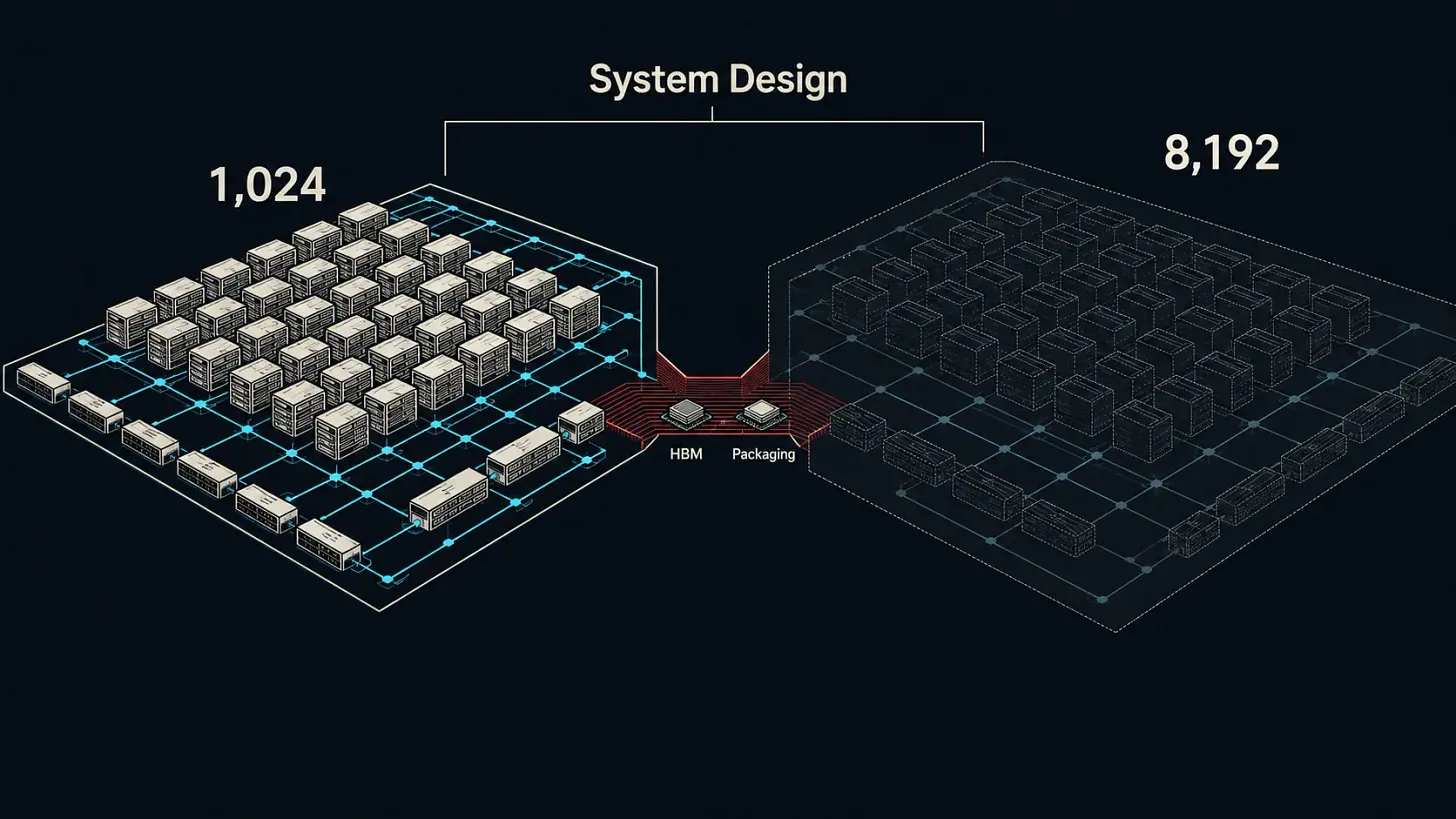
At last year’s World Artificial Intelligence Conference in Shanghai, Huawei stood alone. Its CloudMatrix 384, a system binding 384 AI processors into a single compute fabric, was the exhibition’s centerpiece. No domestic competitor displayed anything comparable.
Twelve months later, the field had inverted. At WAIC 2026, nearly every major Chinese chip and server vendor arrived with a competing supernode design. Moore Threads, a domestic GPU company, showed a 256-GPU system built around a single-layer scale-up fabric. Enflame Technology, an AI chip company, partnered with ZTE on a zero-cable orthogonal design. Biren Technology, a Shanghai-based AI chip startup, introduced optical interconnect targeting 1,024 accelerators. Kunlunxin (Baidu’s chip unit), Lenovo, and others brought competing designs. Huawei unveiled its next generation: the Atlas 950 SuperPoD, with 1,024 Ascend processors on display and a design maximum of 8,192.
The concept now carries a published definition. Pengcheng Laboratory, a national computing research facility in Shenzhen, and the Global Computing Alliance published the first white paper specifying 3 technical requirements for a supernode: memory-semantic access with unified addressing across physical nodes, ultra-low latency, and ultra-high bandwidth. The decisive criterion is whether processors on separate servers can execute load and store operations against each other’s memory, as though they shared the same board.
The competitive unit in China’s AI hardware sector is moving from the chip toward the integrated system. Huatai Securities, a Chinese brokerage, projects the domestic supernode market at Rmb 341.4bn (approximately $50.2bn) by 2028, implying a compound annual growth rate of 194% from 2026.
Why 2026, Not 2025
Two demand-side forces converged this year.
The first is model scale. Moonshot AI, a Beijing-based foundation model company, released Kimi K3 in July with 2.8 trillion parameters. It reportedly requires at least 64 accelerator cards organized as a supernode for deployment. DeepSeek’s V4-Pro pricing page notes that throughput is constrained by compute availability and flags a price reduction once Ascend 950 supernodes ship at scale. As I examined in a previous analysis, the model’s commercial roadmap is explicitly timed to a domestic chip delivery schedule.
The second is a shift in who consumes tokens. AI agents can generate and consume tokens at 100 to 120 per second, several times the 25 to 30 a person reads. A single agent task consumes an estimated 4 times the tokens of a standard conversation, with multi-agent coordination reaching 15 times. That growth raises the value of low-latency, high-bandwidth interconnect inside large clusters, and strengthens the commercial case for supernodes.
The demand case is clear. Whether China’s system-level design lead can hold depends on a harder question: what happens when a supernode’s architecture runs ahead of the components inside it?
Behind the shared label are three different interconnect bets, a component supply chain that has not kept pace with system design, and a utilization problem that better hardware alone will not solve.
Three Interconnect Bets, One Physics Problem
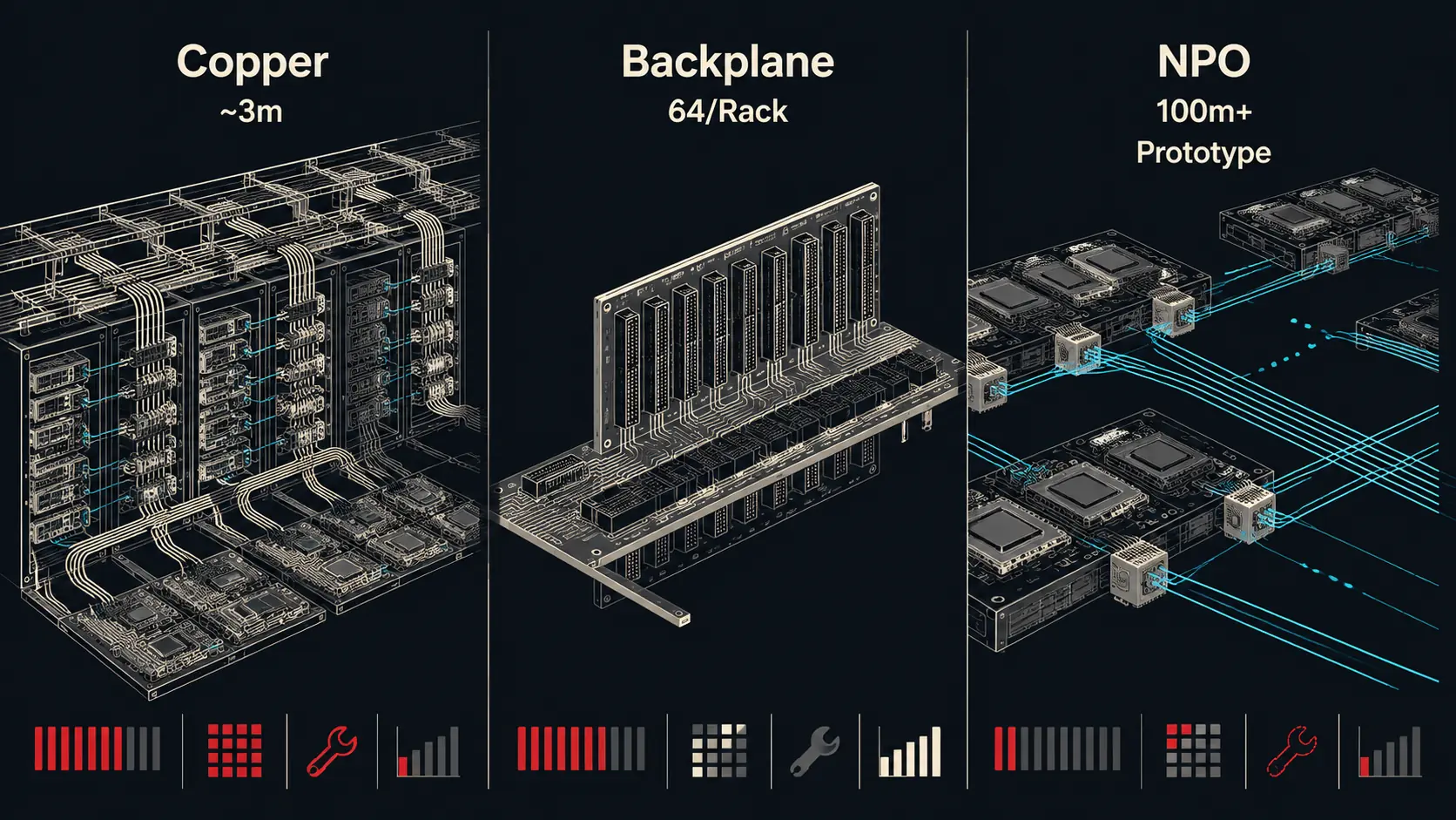
The vendors at WAIC did not converge on a single design. Their products reflect 3 prominent approaches to the same engineering constraint: how to connect hundreds of processors tightly enough that they behave as one machine.
Copper cable trays, exemplified by Moore Threads’ MTT C256, route cables between GPU modules to connect 128 GPUs within one rack and 256 across 2. Moore Threads argues that the design preserves signal integrity and link reliability. The operational cost is a densely cabled system in which servicing failed links becomes a significant maintenance burden.
Orthogonal backplane designs, such as the Enflame-ZTE supernode, eliminate internal cables entirely. Perpendicular connector boards create direct electrical paths, reducing signal attenuation and simplifying maintenance. Current configurations fit 64 accelerators per rack, half the cable-tray density. The design can scale across racks to 512; Enflame says volume production is planned by year-end.
NPO (Near-Packaged Optics), proposed by Biren, mounts optical engines near the processor package. Light replaces electrical signals, extending stable interconnect from meters to hundreds of meters, but NPO remains at the prototype stage, with cost and manufacturing maturity still limiting volume deployment.
Each path bets on which constraint binds first. Copper hits a signal wall at roughly 3 meters at supernode data rates. Orthogonal designs face a density ceiling. Optical interconnect relaxes both constraints but introduces cost and manufacturing risks the industry has not resolved.
Same Conclusion, Opposite Engineering
NVIDIA and China’s supernode builders have both concluded that competitive advantage is migrating from the chip to the system. Their engineering responses diverge.
NVIDIA’s GB200 NVL72 packs 72 Blackwell GPUs and 36 Grace CPUs into one rack, connected by NVLink at 1.8 TB/s per GPU, delivering 720 petaflops of sparse FP8 tensor compute at roughly $3.9m all-in. At MLPerf Training 6.0, Microsoft trained Llama 3.1 405B to target quality in 7.07 minutes on 8,192 GB200 GPUs. It combines dense silicon, high energy efficiency, and mature software.
Huawei inverts the formula. CloudMatrix 384 deploys 384 Ascend processors and 192 Kunpeng CPUs. SemiAnalysis assessed in 2025 that the system was “arguably a generation ahead” in system architecture, despite per-chip performance that trailed both NVIDIA and AMD. SemiAnalysis estimated the cost at roughly 4.1 times the total power of a GB200 NVL72 system, with 2.5 times worse energy efficiency per FLOP.
NVIDIA’s planned response, Rubin Ultra NVL576, would extend the NVLink domain to 576 GPU dies across 8 racks. The original design targeted 15 exaflops FP4 and 5 exaflops FP8 for the second half of 2027, but those figures were based on a 4-die package NVIDIA has since abandoned. SemiAnalysis reported in July 2026 that manufacturing problems pushed the Kyber rack toward 2028. NVIDIA says its roadmap remains intact but has not reaffirmed volume NVL576 shipments in 2027.
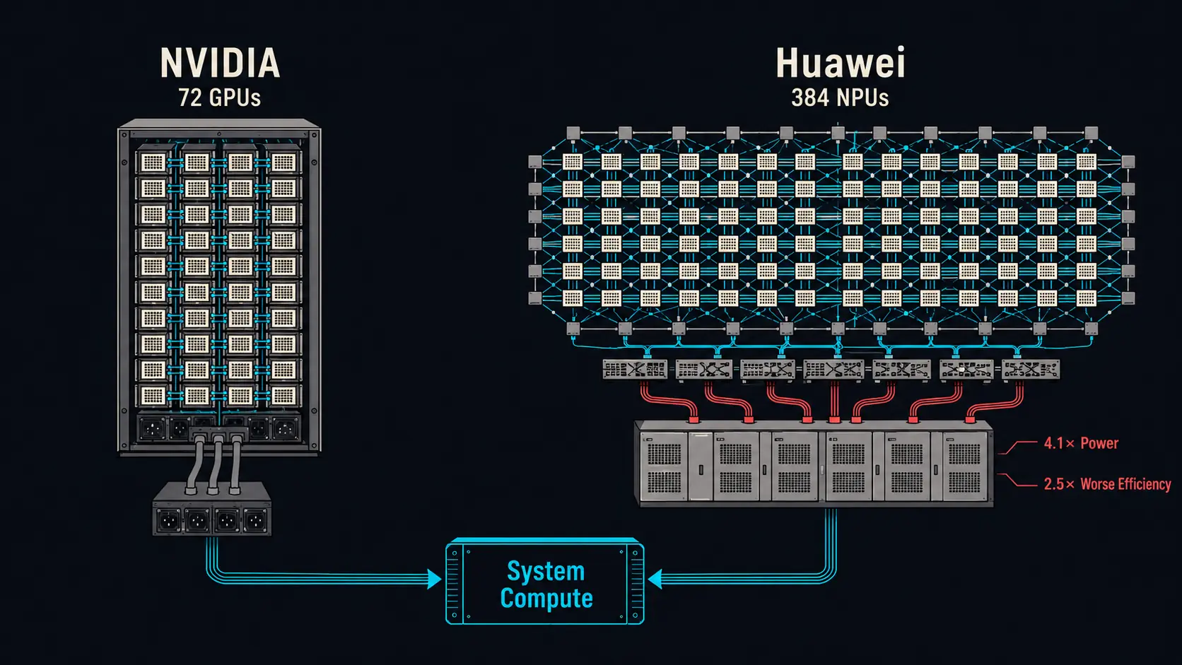
If NVL576 reaches production near schedule, NVIDIA can argue that stronger silicon delivers comparable system compute with far fewer chips. If it slips to 2028 and Huawei ships its 1,024-accelerator Atlas 950 systems at volume, Huawei could hold a 1-to-2-year lead in large-scale compute domains inside China with no Western counterpart in production.
The same system-level shift is changing the balance between accelerators and general-purpose compute. Both NVL72 and CloudMatrix 384 ship with 2 accelerators per CPU, double the CPU content of the prior DGX H100 generation. Intel said in Q1 2026 that deployed ratios had moved from 1 CPU per 8 GPUs toward 1 per 4. AMD expects agentic workloads to push toward 1:1. Reuters reported on July 23 that prices for some server CPUs in China had risen more than 40% since January. The supply constraint has expanded from GPUs and memory to CPUs.
The Component Gap Inside the System
China’s supernode architectures have advanced faster than the supply chains feeding them. The gap is sharpest in high-bandwidth memory.
TechInsights, a semiconductor teardown firm, disassembled multiple Ascend 910C processors, the chip inside the CloudMatrix 384 systems already in deployment. The teardowns found Samsung and SK Hynix HBM2E memory and computing chiplets linked to TSMC fabrication. The deployed systems contain foreign components at their core.
The HBM version of the Ascend 950PR uses what Huawei calls HiBL 1.0, described as self-developed HBM. The label appears to confirm Huawei designed the memory interface. It does not confirm domestic production of DRAM wafers, stacking, or packaging. No independent teardown has been published. CXMT, China’s most advanced DRAM producer and the most likely domestic HBM partner, has moved HBM3 into customer sampling and limited trial production. SemiAnalysis estimates its composite yield at roughly 25%, with monthly wafer allocation rising from about 5,000 at the end of 2025 to a projected 30,000 by the end of 2026. CXMT’s IPO prospectus did not list HBM as a named project.
Two product lines illustrate the constraint differently. The 950PR ships in DDR and HBM versions, at roughly Rmb 50,000 and Rmb 70,000 respectively. Reuters reported Huawei plans to ship approximately 750,000 units of the 950PR in 2026, without specifying the HBM share. Huawei could still meet its unit target by shifting more of the mix toward DDR, but DDR cannot match HBM bandwidth for high-performance training and long-context inference. The Atlas 950 SuperPoD presents a harder test. It uses the Ascend 950DT, a higher-specification chip planned for Q4 2026. On a 4-stack-per-chip assumption, a full 8,192-accelerator system would require roughly 32,768 HBM stacks. There is no public evidence that current domestic production can support repeated deliveries at that scale.
Below HBM in the risk hierarchy: advanced packaging, where Chinese firms have demonstrated 2.5D capability but Huawei has not disclosed its suppliers; high-speed optical components, where module assembly is domestic but many high-end modules still rely on imported DSPs, lasers, and other optical chips; PCIe switching silicon, where Shudu Technology has begun limited production of a PCIe 5.0 switch but has not been publicly identified as a supplier to a major supernode deployment; and liquid cooling, the least exposed category, where domestic suppliers can deliver most system-level hardware.
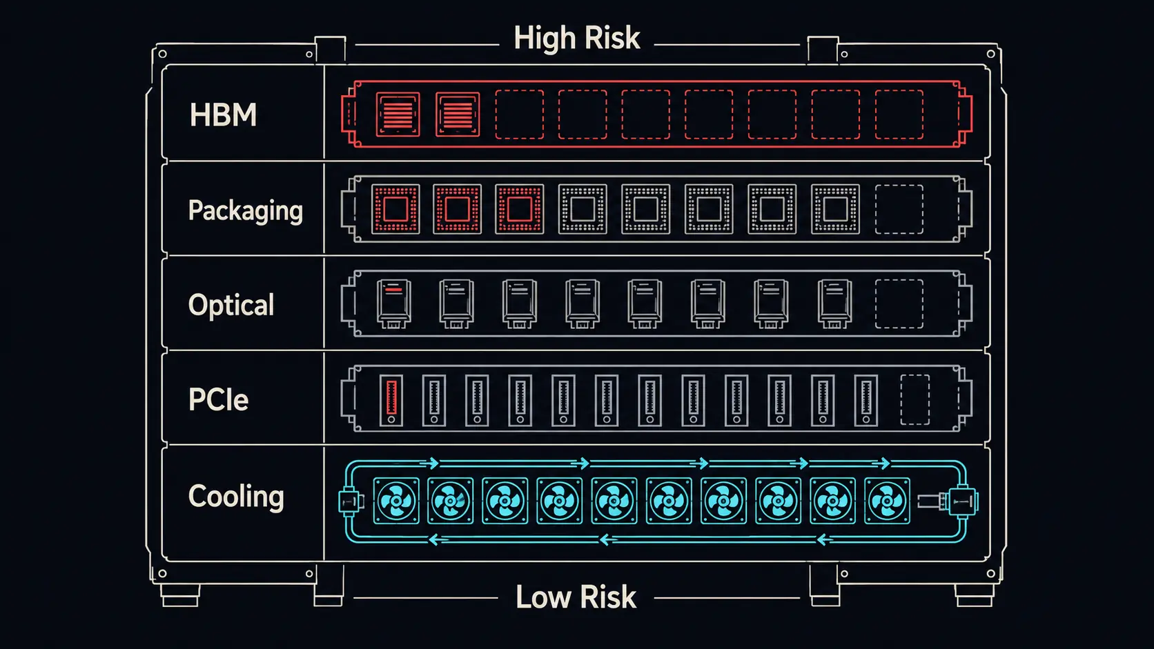
China can design, assemble, and deliver supernodes. It has not yet built a supernode supply chain fully independent of foreign technology.
Who Buys a Supernode
Huawei says more than 750 CloudMatrix 384 systems have entered commercial use. Public evidence confirms real deliveries: the Financial Times reported in 2025 that Huawei had sold and begun delivering more than 10 systems, and Hongxin Electronics, a listed Chinese electronics manufacturer, disclosed a 4-system purchase. SiliconFlow, an inference optimization company, runs DeepSeek-R1 on CloudMatrix 384 in production. These cases confirm real commercial deployment. They do not reconcile to Huawei’s cumulative figure, which lacks an independent audit.
One computing executive estimated that supernodes cost about 50% more than conventional servers while delivering as much as 10 times the performance on suitable workloads. The buyer profile suggests who finds the arithmetic persuasive: state-owned enterprises, telecom operators, financial institutions, and energy and transportation groups. Compliance, data sovereignty, and local deployment appear to drive these purchases more than per-token economics.
The utilization challenge has not gone away. Shanghai Securities News, a state-affiliated financial daily, reported from a national computing center in March 2026 where servers equipped with NVIDIA GPUs had rental rates above 90% while domestic GPU servers sat below 50%. An executive at a Chinese CPU designer said visits to other facilities found that many centers still operated below 30% utilization. Supernodes improve efficiency within a running workload. A Shenzhen research consortium, with Huawei participating in optimization, reported MFU of roughly 30% on a thousand-chip cluster and 34.9% on a supernode; no controlled comparison was published. But supernodes do not generate demand. The low facility-level numbers reflect software ecosystem gaps, workload scarcity, and regional oversupply of capacity no tenant needs. No comparable US-wide figure exists; different studies measure different things. That distinction matters when evaluating whether projected hardware sales will translate into productive capacity.
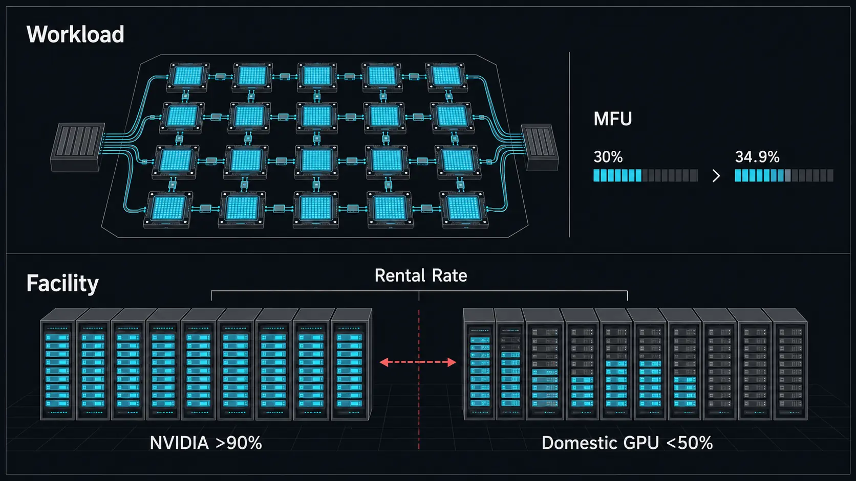
Whether supernodes create economic value depends on utilization. Which systems qualify for procurement may come down to standards.
The Race to Define the Category
The Pengcheng Laboratory white paper proposes standardized capability grading, interoperability requirements, and testing certification. It lacks formal standard status, a mandatory conformance process, and a certified product list. But its core criterion, unified memory addressing with memory-semantic access, aligns closely with the architecture Huawei has already shipped. More than 30 organizations contributed, including Arm China, Baidu, and Cambricon. The framework is not Huawei’s standard. But Huawei holds an early advantage: its existing architecture and published product specifications map directly onto the proposed criteria.
Export controls target chip performance more directly than system architecture or procurement definitions. Yet many of the components those controls restrict remain inside the supernodes China is trying to scale. Chinese vendors and research institutions are working to move AI infrastructure competition from a domain bounded by semiconductor physics to one shaped by system design and standards. If the components inside the racks match the ambition of the architecture around them, that shift could give Chinese infrastructure vendors a structural advantage in procurement. If they do not, the supernode moment will have demonstrated an architectural thesis its own supply chain cannot yet deliver at scale.
第二部分:中文深度解读
一、一句话定位
这不是一篇新闻,而是一份缺口清单:中国 AI 硬件的竞争单元已经从「芯片」上移到「系统」,但这个上移发生得比支撑它的零部件供应链更快——封面图把全书论点画完了:系统设计能把互连域从 1,024 推到 8,192(虚线),而收窄的那个瓶颈上写着两个词:HBM、Packaging。
二、作者的坐标系
全文只有一把尺子:组件是否跟得上架构。所有事实都挂在这一根轴上。
由此推出一个反直觉的因果骨架:
1
2
3
4
5
6
7
8
模型规模(2.8T 参数)+ Agent 消耗 token 的数倍增长
        ↓  需求侧成立
系统设计能力(互连架构)在一代之内追平甚至反超 NVIDIA
        ↓  供给侧不成立
HBM → 先进封装 → 高速光器件 → PCIe 交换 → 液冷
        (风险从高到低,缺口从大到小)
        ↓
架构领先无法转化为可持续的交付能力
注意这条链的终点不是「中国做不出超节点」,而是文中的原话:「中国能设计、能组装、能交付超节点。它还没有建成一条完全独立于外国技术的超节点供应链。」 前后两句都重要——作者没有把话说成「做不到」,说的是「做得到,但底座不是自己的」。
三、超节点的官方定义(这条最容易被略过,其实最硬)
2026 年 7 月,深圳鹏城实验室与全球计算联盟发布了首份白皮书,把「超节点」落成三条技术要求:
| 要求 | 含义 |
|---|---|
| 跨物理节点的统一寻址 + 内存语义访问 | 决定性的那一条 |
| 超低时延 | — |
| 超高带宽 | — |
判决标准是第一条:不同服务器上的处理器,能否对彼此的内存直接执行 load / store,就像在同一块主板上一样。这一条把「超节点」和「一堆用高速网络连起来的机器」彻底分开了——前者是一个内存域,后者只是一个通信域。所有互连路线的优劣,最终都要回到这句话上衡量。
四、三条互连路线:同一个物理约束的三种解法
约束是同一个:怎么把几百颗处理器连到「像一台机器」那么紧。WAIC 2026 上的答案分三派:
| 铜缆托盘 | 正交背板 | NPO(近封装光学) | |
|---|---|---|---|
| 代表 | 摩尔线程 MTT C256 | 燧原 × 中兴 | 壁仞 |
| 连接规模 | 128 GPU(单柜)/ 256(跨 2 柜) | 64 加速器/柜,可跨柜扩至 512 | 目标 1,024 加速器 |
| 稳定距离 | ~3 m(信号墙) | 板级直连 | 米级 → 数百米 |
| 取舍 | 保信号完整性/链路可靠性 | 取消内部线缆、降低衰减、便于维护 | 同时松开带宽与距离约束 |
| 代价 | 密集线缆 → 坏链维护成为负担 | 密度只有铜缆托盘的一半 | 仍处原型阶段,成本与制造成熟度不足 |
| 状态 | 在售 | 燧原称年底量产 | Prototype |
读法:三条路线不是「谁更先进」的排序,而是各自赌「哪个约束先咬人」。铜在超节点速率下约 3 米撞墙;正交背板撞的是密度天花板;光学两条约束都松开,但引入了行业尚未解决的成本与制造风险。图上那组小柱状图(带宽/距离、密度、可维护性、成熟度)已经把权衡画出来了——没有一条路线在所有维度上都赢。
值得单独指出:NPO 出现在这里,是本次最应该与站内光互联系列并读的一点。NPO 正是 CPO 谱系里「光引擎靠近封装但未完全共封装」的中间形态;这篇从系统架构侧给出了它为什么必须存在的理由——不是因为光更先进,而是因为电在 3 米处真的到头了。
五、同一个结论,相反的工程
NVIDIA 与中国的超节点建造者得出了同一个结论(竞争优势正在从芯片迁移到系统),但工程应答完全相反:
| NVIDIA GB200 NVL72 | 华为 CloudMatrix 384 | |
|---|---|---|
| 规模 | 72 GPU + 36 CPU / 柜 | 384 Ascend + 192 Kunpeng |
| 互连 | NVLink,1.8 TB/s/GPU | 自研互连,跨柜 |
| 算力 | 720 PFLOPS(稀疏 FP8) | — |
| 整套价格 | 约 $3.9m | — |
| 能效 | 基准 | 功耗约为前者的 4.1×,每 FLOP 能效差 2.5×(SemiAnalysis 估算) |
| 路线 | 更密的硅、更少的芯片 | 更多的芯片、更松的单芯片指标 |
NVIDIA 的 MLPerf 证据很硬:Microsoft 用 8,192 张 GB200 在 7.07 分钟内把 Llama 3.1 405B 训到目标质量。
而 SemiAnalysis 在 2025 年的判断是:CloudMatrix 384 在系统架构上「可以说领先一代」,尽管单芯片性能落后 NVIDIA 和 AMD。这是全文最重要的一句评价——它把「架构领先」和「芯片领先」明确切开,也解释了后面那个 4.1× 的功耗数字为什么可以同时成立。
真正的胜负手在时间线上:NVIDIA 的 Rubin Ultra NVL576 原本要把 NVLink 域扩到 8 柜 576 颗 GPU die(原目标 2027 下半年 15 EF FP4 / 5 EF FP8),但那些数字基于一个已被放弃的 4-die 封装;SemiAnalysis 2026 年 7 月报道制造问题把 Kyber 机柜推向 2028 年。于是形成一个双分支:
- NVL576 按期量产 → NVIDIA 可以说「更强的硅用更少的芯片达到同等系统算力」;
- 滑到 2028 年,而华为 1,024 加速器的 Atlas 950 规模交付 → 华为可能在中国境内的大规模计算域上握有 1–2 年领先,且没有西方对应产品在产。
⚠️ 请注意那个限定词——「在中国境内」。这是一个被地理切分的市场,「领先」是在一个分区内部度量的。任何把这类数字读成「中国 AI 硬件全面领先」的结论,都越过了作者的限定。
六、加速器 / CPU 的天平在倒转
两条产品线在同一个方向上出了问题:NVL72 与 CloudMatrix 384 都是 2 加速器配 1 CPU,是上一代 DGX H100 世代 CPU 配比的两倍。再往后:
- Intel 2026 Q1:已部署配比从「1 CPU 配 8 GPU」向「1 配 4」移动;
- AMD:预计 agentic 负载会推向 1:1;
- Reuters(7 月 23 日):中国部分服务器 CPU 价格自 1 月以来涨超 40%。
结论:供给约束已经从 GPU 扩散到内存、再扩散到 CPU。 而且配比从 8:1 走到 1:1,意味着每颗加速器要背的 CPU 成本涨了约 8 倍——这部分会直接在超节点的 BOM 里抵消掉一部分「系统架构带来更多算力/芯片」的收益。这一点原文没有展开,但它是理解超节点经济性的必需项。
七、组件缺口:风险阶梯
| 层级 | 现状 | 缺口性质 |
|---|---|---|
| HBM | 风险最高。Ascend 910C 拆解(TechInsights)发现 Samsung / SK Hynix HBM2E,计算 chiplet 仍指向 TSMC 工艺 | 已部署系统的核心是外国件 |
| 先进封装 | 已展示 2.5D 能力,但华为未披露供应商 | 能力存在,链条不透明 |
| 高速光器件 | 模块组装国产,高端模块仍依赖进口 DSP、激光器与其它光芯片 | 组装在内,芯片在外 |
| PCIe 交换 | 数渡科技已小批量产 PCIe 5.0 交换芯片,但未被公开确认为任何大超节点的主要供应商 | 有无之间 |
| 液冷 | 暴露最少,国产供应商能交付大部分系统级硬件 | 基本可控 |
这个阶梯读起来像「风险排序」,但它其实是一张价值密度图。 缺口最大的 HBM 与先进封装,恰好是整条链上毛利与壁垒最高的两层;缺口最小的液冷,恰好是最不依赖 IP 密度的一层。所以「液冷不受制于人」并不是因为中国在这层特别强,而是因为这层本来就没有多少可守的东西。缺口的形状等于价值链的形状——这是原文没有说、但从它的排序里必然导出的一条。
HBM 这一层的细节(全文技术含量最高的部分)
- 950PR 的 HBM 版本用华为自称的「HiBL 1.0」,被描述为自研 HBM。 作者的处理非常克制,值得学:这个标签只能确认华为设计了内存接口,不能确认 DRAM 晶圆、堆叠、封装的国产化。且没有任何独立拆解报告发表。
- CXMT(国内最先进的 DRAM 厂、最可能的 HBM 伙伴)HBM3 已进入客户送样与有限试产。SemiAnalysis 估算其综合良率约 25%;月晶圆投入从 2025 年底约 5,000 片升至 2026 年底预计 30,000 片。注意——CXMT 的 IPO 招股书没有把 HBM 列为具名项目。
- 950PR 双版本:DDR 版约 5 万元、HBM 版约 7 万元。Reuters 报道华为 2026 年计划出货约 75 万颗 950PR,未说明 HBM 占比。作者点破了这个数字的漏洞:华为可以通过把配比更多移向 DDR 来完成出货量目标——但 DDR 在带宽上无法匹配高性能训练与长上下文推理。
- 真正的硬测试是 Atlas 950 SuperPoD:它用计划 2026 Q4 的 Ascend 950DT。按每芯片 4 stack 假设,一个完整的 8,192 加速器系统需要约 32,768 个 HBM stack。没有任何公开证据表明当前国内产能能支撑这种规模的反复交付。
八、需求侧真相:谁买,以及利用率
谁在买:国企、电信运营商、金融机构、能源与交通集团。一位计算行业高管估计超节点比常规服务器贵约 50%,在合适负载上性能可达 10 倍。购买驱动更多是合规、数据主权、本地化部署,而不是每 token 经济性。
这一点必须正面说出来:需求是被政策塑造的,不是被经济学塑造的。 好处是它不会因为效率不佳而消失;代价是它也不会因为效率不佳而被纪律约束。这两面同时成立。
用量证据要分开看:华为称超过 750 套 CloudMatrix 384 已进入商用;而公开可核的证据是——FT 报道华为已售出并开始交付超过 10 套、上市公司宏芯电子披露采购 4 套、SiliconFlow 在生产中用它跑 DeepSeek-R1。公开证据与 750 这个累计数字之间差了大约两个数量级,且后者没有独立审计。 作者如实写了这一点,没有替谁圆场。
然后是最难受的一节——利用率:
| 层面 | 数字 | 出处强度 |
|---|---|---|
| 工作负载(MFU) | 千卡集群约 30% → 超节点 34.9% | 深圳某研究联合体(华为参与优化),未发表对照实验 |
| 设施(租赁率) | NVIDIA GPU 服务器 >90%;国产 GPU 服务器 <50% | 《上海证券报》2026 年 3 月,某国家算力中心 |
| 设施(利用率) | 某国产 CPU 设计公司高管称,走访发现许多中心仍低于 30% | 单一口径,访谈性质 |
把前两行并排读,会得到一个原文没有明说、但比它所有论断都尖锐的结论:架构带来的 MFU 提升是约 5 个百分点(30% → 34.9%),而设施层的租赁率差距是约 2 倍(>90% vs <50%)。 也就是说,如果能把软件生态与负载供给的问题解决,能拿到的收益大于超节点架构本身提供的收益。超节点在一个正在运行的负载内部提高效率(作者原话),但它不产生需求。设施层的低数字反映的是软件生态缺口、负载稀缺与区域性产能过剩——这三样东西,再好的硬件也修不了。
(作者在此处还加了一句很诚实的限定:不存在可类比的美国全国性数字,不同研究测的东西不同。这句话应该被保留——它挡住了「美国利用率多少」这类没有答案的追问。)
九、标准之争:最容易被低估的一节
鹏城实验室的白皮书提出能力分级、互操作要求、测试认证。作者立刻标注了它的三个”还没有”:没有正式标准地位、没有强制符合性流程、没有认证产品清单。
但接下来一句才是关键:白皮书的核心判据(统一内存寻址 + 内存语义访问)与华为已经出货的架构高度对齐。超过 30 家机构参与,包括 Arm China、百度、寒武纪。这个框架不是华为的标准;但华为握有早期优势——它已有的架构与已公布的产品规格,直接映射到这套被提议的判据上。
我的评述:谁掌握「能力分级 + 符合性认证 + 认证产品清单」,谁就掌握了采购入口。白皮书目前没有强制力,但它正在被已部署产品反向追认——先有能跑的产品,再有追认它的标准,而不是先写标准再按标准造产品。NVLink / InfiniBand 生态的成型路径与此同构。原文把这段放在结尾、篇幅很短,我认为它的战略分量被低估了:架构领先只有被写成判据才算兑现。
最后一个结构性张力,作者点得很清楚:出口管制直接瞄准的是芯片性能,而不是系统架构或采购定义。 但管制清单上被限制的很多组件,仍然装在中国正试图规模化的那些超节点里。这句话其实是全文的闭环——管制打的是「芯片」这颗棋子,而中国下的棋是把竞争挪到「架构与标准」这个棋盘上;可棋盘换了,棋子还是原来的棋子。
十、可采信度分层
| 强度 | 内容 | 理由 |
|---|---|---|
| 强 | 华为 Atlas 950 规格(1,024 展示 / 8,192 设计上限)、NVIDIA GB200 NVL72 规格、MLPerf 6.0 的 7.07 分钟、950PR 两版价格(5 万 / 7 万元)、白皮书三条要求 | 一手规格或可复现基准 |
| 中 | SemiAnalysis 的 4.1× 功耗 / 2.5× 能效、TechInsights 的 910C 拆解结论、Reuters 的 CPU 涨价 40%、FT 的交付数量、上证报的租赁率、CXMT 良率约 25% | 第三方估算或可信媒体报道,但均为估算而非测量 |
| 弱 | 华为「750+ 套已商用」、HiBL 1.0「自研 HBM」的推论、某高管「贵 50% / 快 10 倍」、MFU 30% / 34.9%、「许多中心低于 30%」 | 厂商自述、单一口径、无对照、无审计 |
| 无法核实 | Ascend 950 的 HBM 无独立拆解、白皮书无认证清单、Huatai 的 341.4bn 预测无中间假设、无可类比的美国全国利用率 | 数据本身不存在或不公开 |
十一、两个数字之间的账,原文没有对上
这是我在通读时发现的一处内部张力,值得单独列出:
- 一处说:超节点比常规服务器贵约 50%,在合适负载上性能可达 10 倍;
- 另一处说:CloudMatrix 384 的总功耗约为 GB200 NVL72 的 4.1 倍,每 FLOP 能效差 2.5 倍。
这两个数并不直接矛盾——前者说的是通信密集的合适负载,后者说的是可比系统算力下的通用能效。但它们出现在同一篇文章里、且从未被对照说明,读者很容易拿「50% 成本换 10 倍性能」去做选型判断。「合适负载上 10 倍」不是可用的规划数字:它没有说明适用负载占比多大、也没说明那 10 倍相对于什么基线(同柜还是同功耗同成本)。这处要在引用时额外小心。
十二、这篇文章没有回答什么
- HBM 国产化的时间线:只有「约 25% 良率」与「5,000 → 30,000 片/月」两个第三方估计,没有产能爬坡的节点表。
- 超节点的 BOM 结构:HBM 占多少、光学占多少、CPU 占多少,全篇没有一个成本拆分——而这恰恰是判断「架构收益能否兑现」的前提。
- 如果 HBM 拿不到,路径是什么:接受 DDR 降级、继续外购、还是等国产,三条路的代价没有被评估(作者只指出华为可以用 DDR 配比完成出货目标,但没有说那样做的性能损失是多少)。
- MFU 提升的归因:30% → 34.9% 有多少来自互连架构、多少来自华为参与的软件优化,无从判断;而没有对照实验,这个数字无法用于任何跨系统比较。
- NPO 何时能跨过成本/良率门槛:只有「prototype」一个状态描述。
- 交付时间点:文章写于 2026 年 7 月 28 日(WAIC 之后),Atlas 950 的 1,024 是「在展台上」、8,192 是「设计上限」——展示不等于交付。第一批 Atlas 950 的实际交付时间,文中没有给出预期。
十三、由文中数字顺手推出的一件事
Huatai 的预测是:2028 年国内市场 Rmb 341.4bn(约 $50.2bn),对应 2026 年起 194% 的复合年增长率。194% 的年增长意味着每年乘以约 2.94 倍。反推:
1
2
3
2028:  341.4 bn RMB
2027:  341.4 / 2.94  ≈ 116  bn RMB
2026:  116   / 2.94  ≈ 39.5 bn RMB
也就是说,这个预测隐含的2026 年基座只有约 Rmb 39.5bn——超节点今天还只是一小块。这份预测押的不是当下体量,而是一条极陡的爬坡曲线。 把这一点与前面「公开可核的交付量级是十几套」并排看:预测的可信度不取决于需求侧(需求侧的故事很好讲),而完全取决于第七节那张组件缺口表能不能在两年内填上。3414 亿这个数字,测的是供应链,不是市场。
十四、与站内文章的联系
- NPO / 光互连:本文的第三条互连路线(壁仞 NPO,目标 1,024 加速器)就是本站在跟踪的 CPO/NPO 谱系的系统侧动机。关于 NPO 的分层定义与标准化进程,见 华为 OIF NPO 标准化与 7.2T 模块 与 NewPhotonics 谈 CPO/NPO 路线;模块级测试与电气链路的度量见 CPO 模块级测试 与 NPO 光电器件链路实验室。
- CPO 的系统级全景:本文「电域先撞墙(~3 m)」与 CPO 224Gbps+ 全栈综述 里「driver/TIA 常是带宽短板、瓶颈清单里几乎没有『光』」是同一个判断的两个视角。
- HBM 层:HBM5 互连的信号完整性 讲的是 HBM 再往上走速率时传输线效应与 PSIJ 挤压抖动预算——正是本文「HBM 是最高风险层」的技术原因。
- 互连与 LLM:Cache-to-Cache 讨论的是把 KV-Cache 在模型之间直连传输,属于同一个「互连带宽决定上层能力」的命题,并且同样卡在「跨节点传输成本未被评估」这件事上。
- 推理系统侧:超节点要解决的「多卡如何像一个域」与本站推理系列的 并行策略 是同源问题;MFU 的定义与测量可参照 推理性能基准,国产加速器栈的背景见 Ascend NPU。
十五、一句话结论
这份材料的价值不在「中国超节点很多」这个事实,而在它把「架构领先」与「供应链自主」拆成了两件必须分别成立的事——并用一张风险阶梯表指出:缺口的形状,就是价值链的形状。如果只从这篇文章带走一个判断,应该是这个:当采购由合规与主权驱动、而不由每 token 经济性驱动时,架构的优势不需要被证明;但同样地,供应链的缺口也不会被市场惩罚——它只会在交付的那一刻一次性显形。
本文为独立撰写的中文深度解读,观点与质疑属解读者本人,不代表原作者立场。英文原文部分为公开内容的完整转载,版权归原作者所有。