The Battle for the Next AI Memory Architecture — 中文解读
Silicon Atlas 把下一代 AI 内存拆成七条路径,按数据距离与移动频率重新框定 zHBM、PIM、CXL 与光链路的定位。
来源:Silicon Atlas — The Battle for the Next AI Memory Architecture 原文链接:https://siliconatlas.substack.com/p/the-battle-for-the-next-ai-memory 原文发布日:2026-08-16 | 作者:Silicon Atlas 说明:本文为英文原文全文转载,附中文结构化解读。原文以英文写就,未作翻译;解读部分为整理归纳,不代表原作者观点。
第一部分:正文(Original Article)
AI memory is often discussed as if zHBM, PIM, HBF, CXL, and optical links were competing for the same position. I do not think that is the best way to compare them. They work on different parts of the data path. Some shorten a package-level connection. Some remove a copy. Others add capacity farther away or reduce the amount of data that needs to move.
As an engineer, I find it more useful to start with two questions: Which data needs to stay close to compute? And how often does it move?
Part 1 looked at Samsung’s zHBM idea, which puts HBM above an accelerator to shorten the last millimeters of the data path. That is one possible answer. This article steps back and looks at the other distances in the system.
A good memory system does not need every byte in the fastest memory. It needs each byte in the right place at the right time.
I use hot data to mean data that is accessed often or has a tight latency limit. Colder data can sit in a slower and more distant tier, as long as software moves or prefetches it before the processor needs it.
Seven Approaches to the Same Problem
There is no single direction. The seven approaches below attack different parts of the same problem.
1. Bring Memory Above Compute
Samsung zHBM would place HBM above an AI accelerator. This shortens the final horizontal path between memory and compute. At FMS 2026, Samsung showed concept models and shared large targets: about 8x the performance of HBM5, more than 10x the memory density, 3x the energy efficiency, and over 50% lower thermal resistance.
Those numbers come from Samsung. They are targets for a future architecture, not measurements from a shipping product. Samsung also did not publish the full system boundary or test method.
For now, zHBM is still a concept and roadmap. There is no sampled product. SAIMEMORY and Intel ZAM are also working on 3D DRAM bonding and target commercialization in fiscal 2029, although public information does not show that their physical design is the same as zHBM. The possible gain is large. So are the open problems: heat removal, bonded-stack yield, power delivery, repair, and customer co-design.
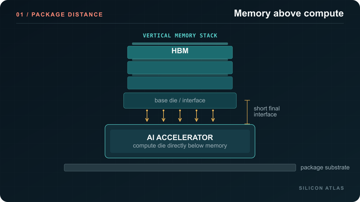 图01|原文配图(Silicon Atlas)
Caption: Approach 1 shortens the final HBM-to-xPU package route by placing memory above compute. Conceptual illustration, not to scale.
2. Move Compute Toward Memory
Instead of moving all data back to a GPU, PIM moves a small amount of compute closer to the data. Samsung HBM-PIM calls this Processing-in-Memory (PIM). SK hynix GDDR6-AiM uses the name Accelerator-in-Memory (AiM). In both cases, selected operations run inside or near the memory banks.
Samsung reported 2x performance and 70% lower energy in a selected system. That does not mean every GPU workload can move into memory.
SK hynix went beyond a standalone chip demo in 2025. It showed a server with two NVIDIA H100 GPUs and four AiMX accelerator cards. The system separates memory-bound and compute-bound parts of LLM inference. This is useful prototype evidence, but we still do not have public customer deployments, independent workload measurements, or a general programming model. PIM makes the most sense when a limited set of operations can run near data without causing problems with precision, coherence, or software.
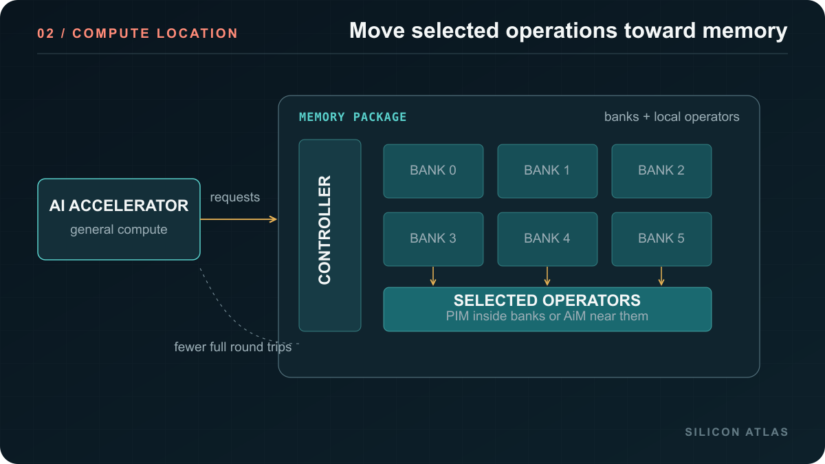 图02|原文配图(Silicon Atlas)
Caption: Approach 2 executes selected operations inside or near memory banks to reduce memory-compute round trips.
3. Let CPUs and GPUs Share Memory
AMD MI300A lets its CPU and GPU dies use the same HBM pool. Apple introduced Unified Memory with M1 in 2020, before the current wave of LLM memory pressure. The products are built for different systems, but the basic benefit is similar: fewer copies between separate CPU and GPU memories.
This is already a mature pattern. LLNL lists El Capitan as a production system with 46,080 MI300A accelerators.
Shared memory does not remove all data movement. It also does not remove capacity limits or competition for bandwidth. Location still matters. A CPU and GPU may share one address space, but an access across the wrong socket or NUMA domain will still be slower. Unified memory removes many explicit copies. It does not make every byte equally close.
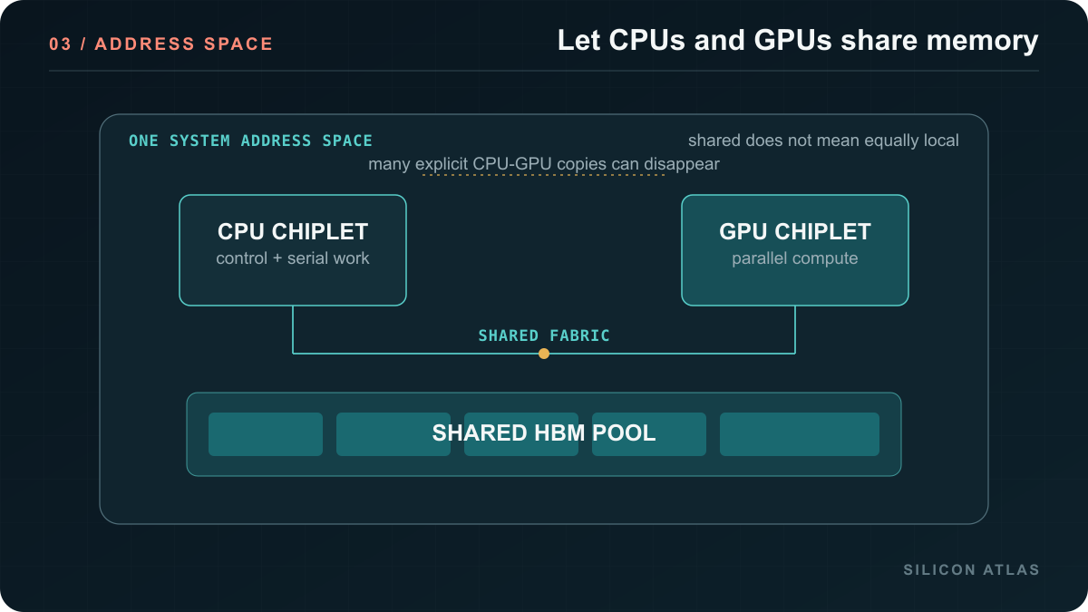 图03|原文配图(Silicon Atlas)
Caption: Approach 3 lets CPU and GPU dies address a shared memory pool, reducing many explicit copies without making every access equally local.
4. Put More SRAM Next to Compute
Cerebras WSE-3 puts 44 GB of SRAM on a wafer-scale processor. Data that is reused can stay close to compute instead of making repeated trips to external memory.
This is no longer only a research idea. Cerebras runs a commercial inference service and says AWS will deploy CS-3 systems in its data centers. Still, it is mature only inside a specialized Cerebras system. It is not a general replacement for a GPU. SRAM takes a lot of area and has limited capacity, so large models still need external memory. A model larger than one wafer must also be split across systems.
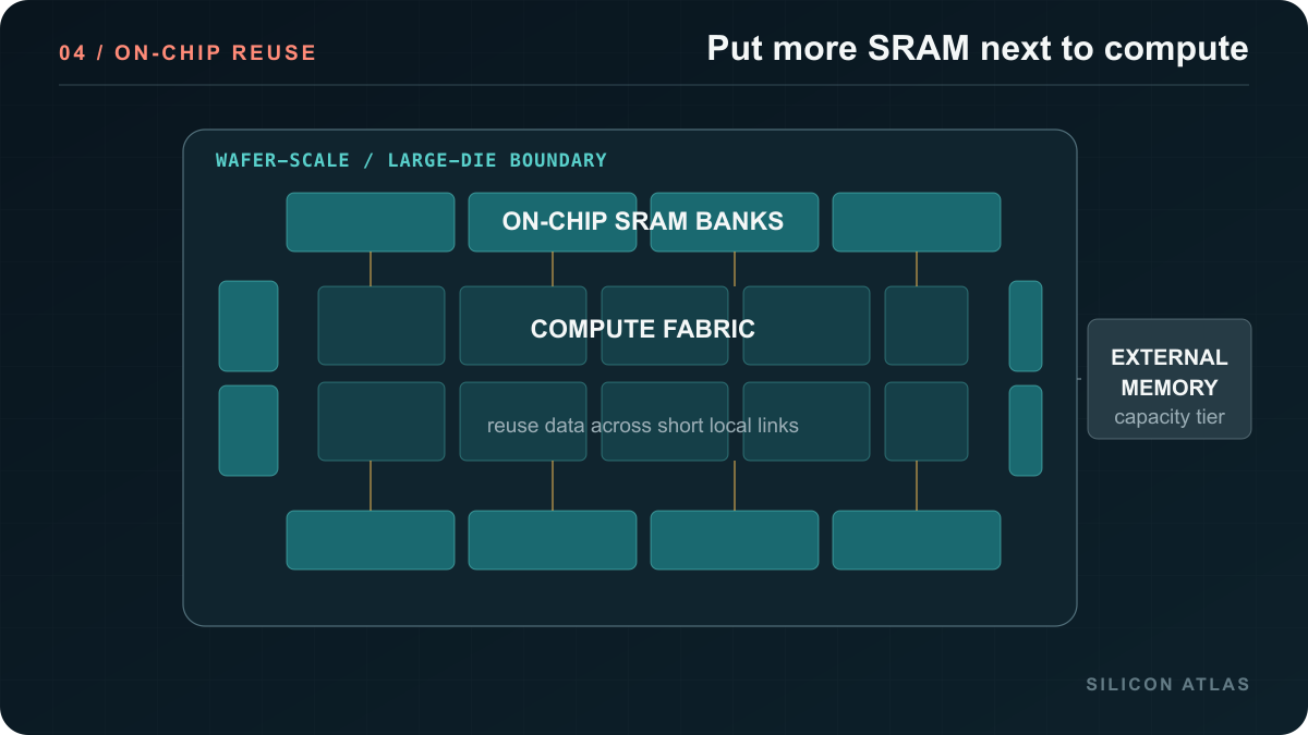 图04|原文配图(Silicon Atlas)
Caption: Approach 4 surrounds compute with a large pool of on-chip SRAM so reused data avoids repeated trips to external memory.
5. Add a Slower but Larger Tier
The simplest way to picture this approach is as several capacity choices. HBM keeps the small working set that needs the highest bandwidth. The HBF approach from SK hynix and Sandisk proposes a larger, package-near NAND tier for read-heavy data that does not fit in HBM. SSD gives much more capacity, but through a slower storage path. An accelerator could use HBM, HBF, and SSD as parallel tiers and choose among them.
HBF connects its NAND stack through a UCIe die-to-die link. Compute Express Link (CXL) solves a different capacity problem. CXL is a family of protocols that runs over the PCIe physical layer. Its CXL.mem protocol lets a CPU access attached DRAM with normal load and store operations in a coherent system address space. Software does not have to treat it like block storage behind an SSD stack.
But the CXL memory is still farther from the CPU. Requests pass through a controller and a serial link. In practice, it acts more like a slower NUMA tier than local DRAM or HBM. HBF adds a package-near NAND tier. CXL extends memory to board or switched-fabric distance. Both add capacity, but in different places.
They are also at different stages. HBF has a public specification and an older sample timetable, but no public measurements from silicon. Sandisk did not repeat that timetable at its latest Investor Day. CXL memory is further along. Micron has reported qualification samples of its CZ120 expansion modules, and CXL 3.2 adds tools such as hot-page monitoring and memory-device management. The hardware alone is not enough. The OS, runtime, and application still need to keep latency-sensitive pages in the right tier.
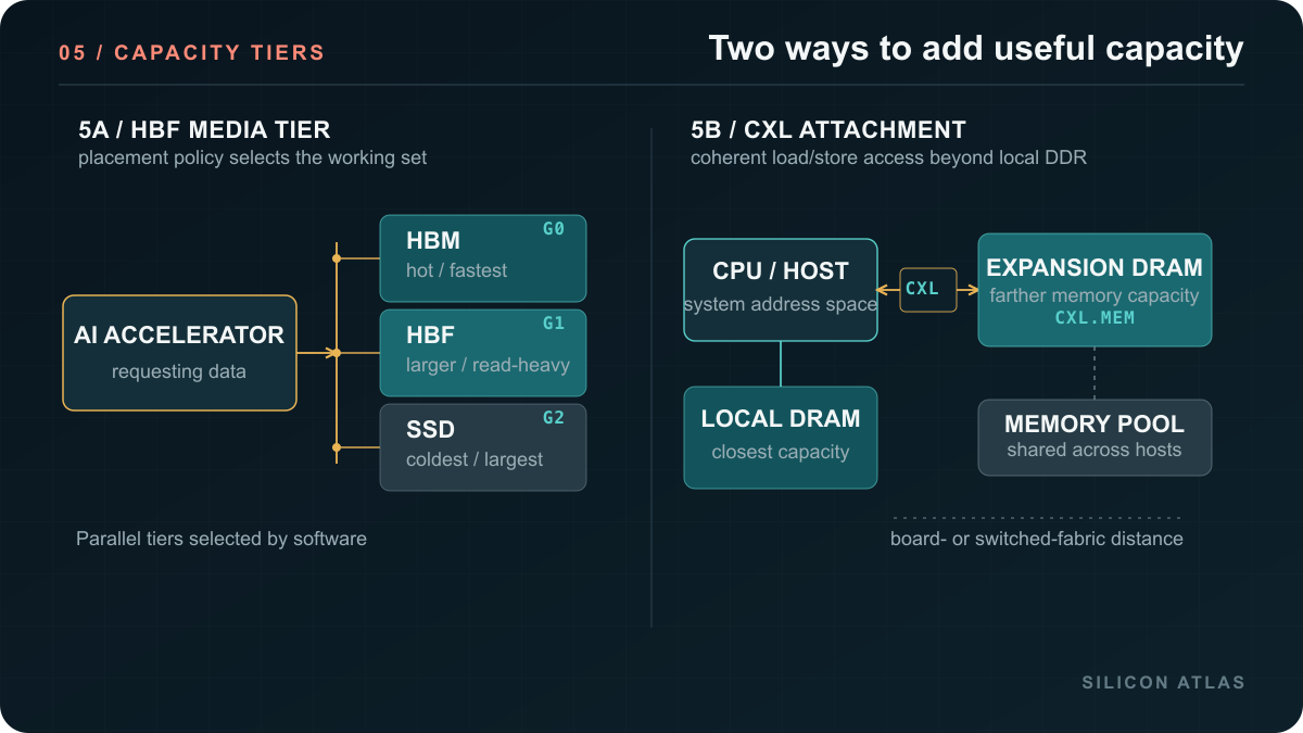 图05|原文配图(Silicon Atlas)
Caption: Approach 5 has two capacity paths: an accelerator selects among parallel HBM, HBF, and SSD tiers, while CXL.mem attaches expanded or pooled DRAM over a coherent host link.
6. Use Optics for Longer Distances
Electrical links become harder to drive as distance and data rate increase. Equalizers and retimers help, but they also use power. NVIDIA CPO and Marvell’s Photonic Fabric use optics for longer board- and rack-scale links. Inside a package, a short electrical link can still be the better answer.
The first production use is showing up in networking. NVIDIA says its Spectrum-X Ethernet Photonics switches are now in production. Optical memory fabrics are at an earlier stage. Marvell expects initial Celestial AI revenue in the second half of fiscal 2028. So the near-term case for optics is stronger in switch and network links than in the short path between a compute die and its local memory.
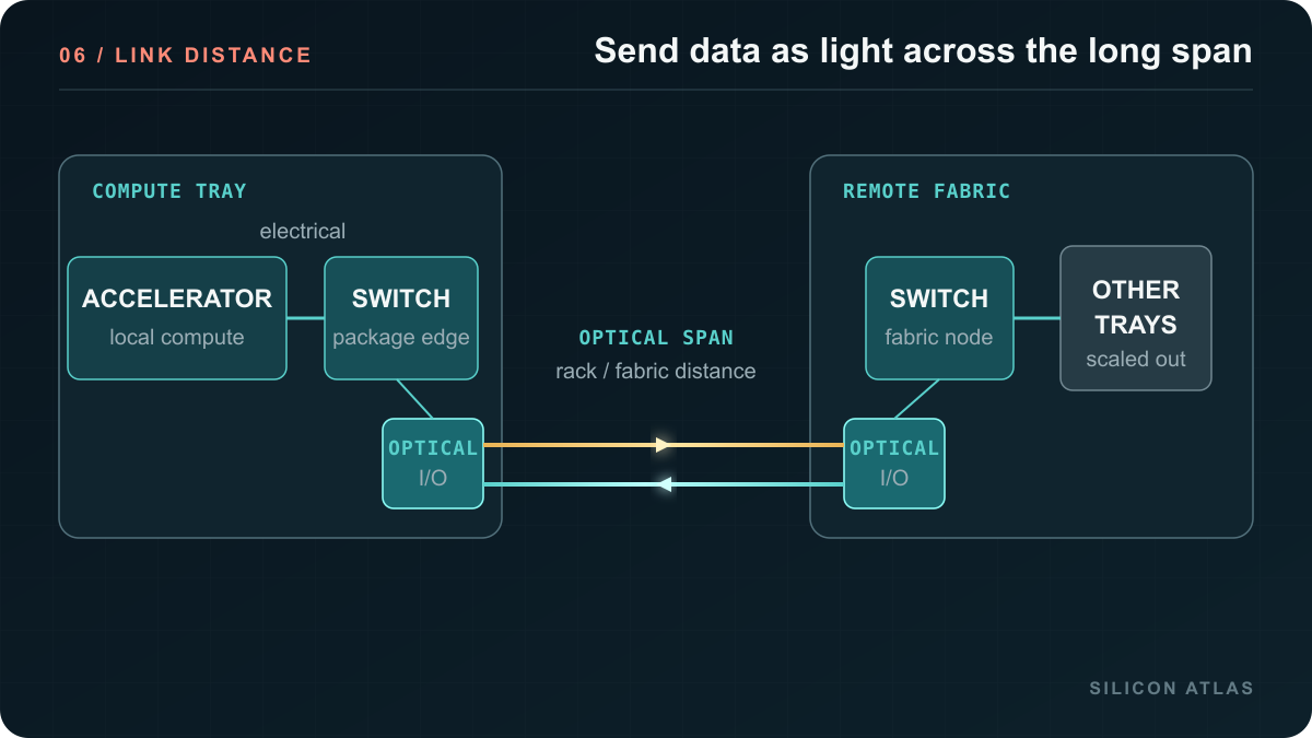 图06|原文配图(Silicon Atlas)
Caption: Approach 6 uses optics for longer board- and rack-scale links where electrical equalization and retiming become costly.
7. Reduce the Bytes That Move
There is another option: move fewer bytes through the same hardware. Quantization uses fewer bits for each value. Pruning removes work or data that has little effect. Selective loading fetches only the weights needed at that moment.
The Apple LLM in a Flash paper studies selective loading for sparse-model weights. It is still research. Quantization, on the other hand, is already used in products. Apple’s 2025 on-device foundation model uses 2-bit weight compression, 4-bit embeddings, and an 8-bit KV cache. Adapters help recover quality. Qualcomm also points to quantization, pruning, smaller models, and full-stack optimization for commercial on-device inference.
This approach usually needs less new hardware than the others in the table. The trade-off depends on the workload. Lower precision can hurt accuracy, and selective loading can make the runtime more complex.
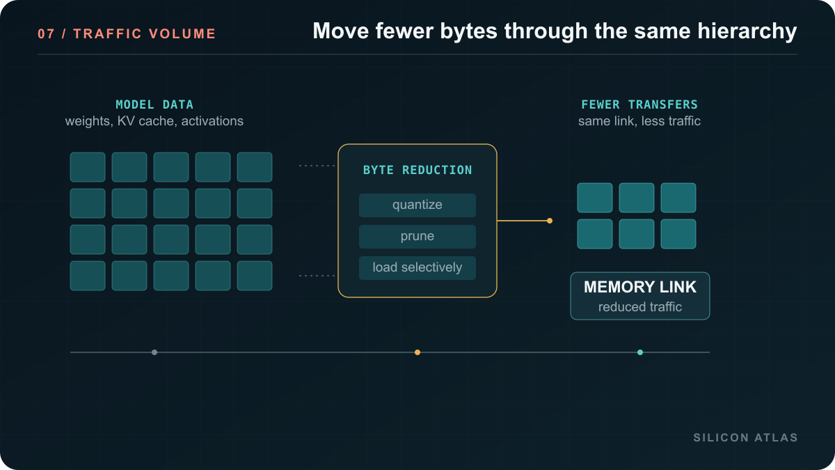 图07|原文配图(Silicon Atlas)
Caption: Approach 7 reduces bit width or transfer count so fewer bytes travel through the same memory hierarchy.
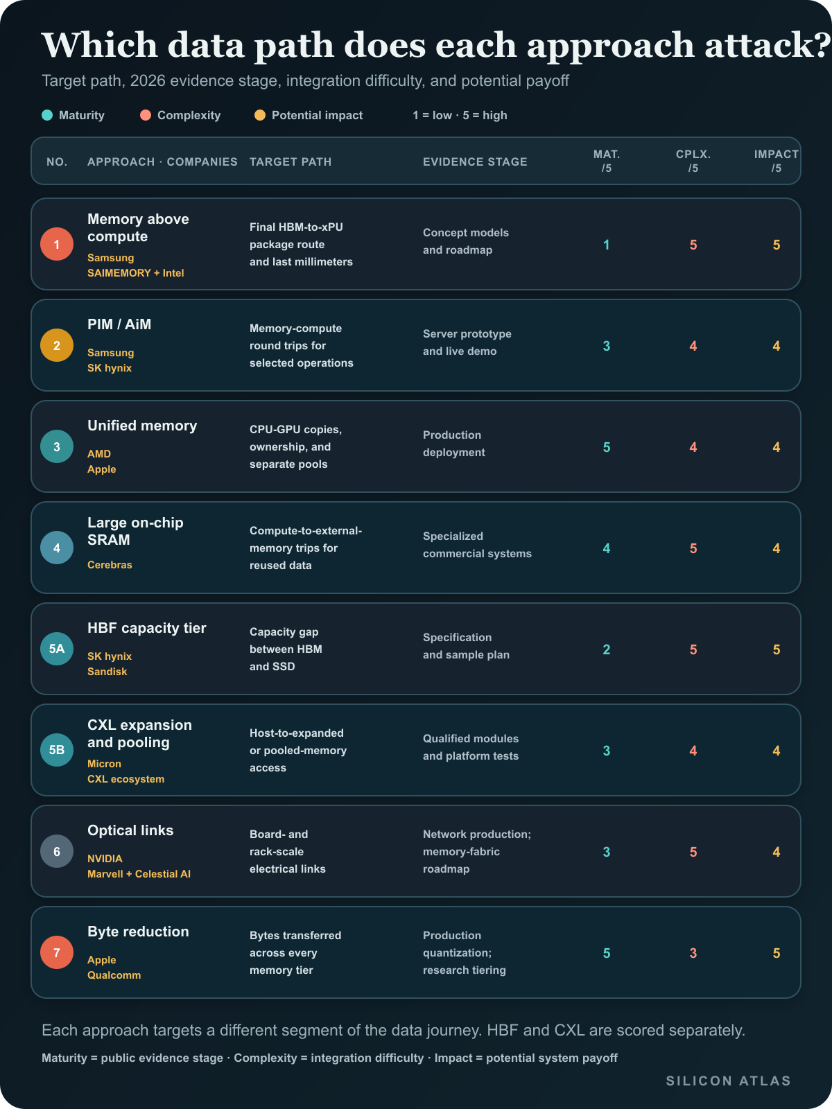 图08|原文配图(Silicon Atlas)
Caption: Each approach targets a different segment of the data journey. Silicon Atlas editorial assessment as of August 2026: maturity measures public evidence stage; complexity measures integration difficulty; impact measures potential system payoff. Scores are directional, not benchmark results.
How I use the impact score: it is my estimate of the possible system benefit if an approach works for its target data path and workload. It is not a market forecast. It also does not mean that the whole system will improve by the same amount.
Each Approach Changes a Different Distance
Memory close to compute usually gives lower latency and lower access energy. The cost is capacity and silicon area. A larger tier can hold more data, but software has to do more work. It must decide what to place there and when to prefetch it.
Each approach changes a different distance. PIM changes where some operations run. Unified memory removes many explicit copies between processors. Optics makes longer board- and rack-scale links less expensive to drive. CPO and zHBM are not direct competitors. They work on different physical paths.
I also separate HBF and CXL in the scorecard, even though both appear in approach 5. HBF asks if a vertically connected NAND stack can work as a high-bandwidth capacity tier. CXL asks if a coherent host link, a memory device, and software placement can make remote capacity useful. The two may work together in a future system. Today, however, a specification-stage HBF stack should not get the same maturity score as a qualified CXL memory module.
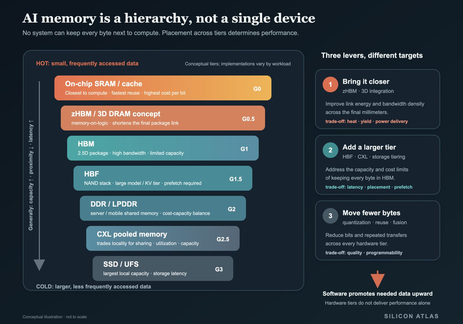 图09|原文配图(Silicon Atlas)
Caption: G0-G3 are conceptual tiers. Real ordering and boundaries vary with interfaces, workloads, and software placement.
HBF Is About Keeping Only the Necessary Data Close
As models and KV caches grow, it becomes expensive to keep every byte in HBM. Capacity is also limited. A practical system needs to separate data that will be used soon from data that can wait. Then it can place each group in a different tier.
SK hynix and Sandisk announced the first HBF specification at FMS 2026. HBF connects a vertical stack of NAND dies to a logic base die. The goal is a capacity tier between HBM and SSD. The announced options include 8-high and 16-high stacks, capacity up to 512 GB, and three bandwidth levels from about 0.4 to 3.0 TB/s. The specification also covers UCIe processor links and gives guidance for packaging, reliability, and software I/O.
Sandisk still included HBF in its AI inference strategy at its August 13 Investor Day and in the presentation. That shows continued interest. It does not show that HBF has passed product validation.
The latest company-confirmed schedule I found is older. In August 2025, Sandisk and SK hynix targeted first Sandisk HBF memory samples in the second half of 2026 and AI inference device samples in early 2027. Sandisk did not repeat those dates at its August 2026 Investor Day. I therefore treat them as an old target, not as a current delivery confirmation. Recent trade press has reported a later commercialization window, but Sandisk has not confirmed a new schedule.
The standards work is becoming more concrete. SK hynix says the first specification was shared through OCP and covers electrical connections, reliability, packaging, and software I/O. OCP’s public directory lists a High Bandwidth Flash Workstream. SK hynix also says Google and Tenstorrent are taking part.
That is more than a slide with an idea. But we still do not have public measurements from silicon or an available product. The 512 GB capacity and 0.4 to 3.0 TB/s bandwidth figures are announced target ranges. Detailed test methods and workload results are not public.
Known: Target position in the hierarchy, stack configurations, maximum capacity, bandwidth grades, UCIe adoption, the published scope of the first specification, the OCP workstream, and the announced sample timetable.
Unknown: Random-read and tail latency, access granularity, sustained write performance, endurance, useful bandwidth, power, and thermal conditions.
These unknowns will decide what HBF can really do. Large and mostly read-only data, such as model weights, may hide NAND latency with parallel access and prefetch. Irregular reads are harder. Data that changes often may also run into page-size, write-performance, or endurance limits. My current view is that HBF is more likely to become a software-managed capacity tier than a direct replacement for HBM.
zHBM tries to shorten the last millimeters for the hottest data. HBF and CXL give colder data another place to live. A future system could use all of them for different working sets.
On-Device AI Repeats the Problem Inside a Smaller Budget
The same memory problem appears in a phone, but the limits are much tighter. The processor shares power and cooling with the modem, camera, display, and battery. There are no hundreds of watts or liquid cooling. Across UFS, LPDDR, system cache, and NPU local memory, copies, reuse, precision, and placement all have to fit inside one small shared budget.
- Shrink the data: Quantization, sparsity, and smaller models reduce weight and activation movement.
- Reuse it nearby: SRAM, cache tiling, and operator fusion reduce repeated LPDDR reads.
- Fetch selectively: Loading and prefetch can use UFS as a supporting tier.
- Follow thermal state: NPU and memory clocks must remain efficient after the device heats up.
In MobileQuant’s Galaxy S24 experiments, W8A8 reduced latency and task energy compared with W8A16 in parts of prefill and decode. Smaller activations reduced memory traffic as well as computation. The result is useful, but the study tested one device and one Qualcomm HTP path. It did not track long-term thermal behavior.
LLM in a Flash is another interesting direction. It loads only the weights needed by a sparse model. However, the paper used an Apple desktop for its evaluation. It does not prove sustained performance on a fanless phone.
Apple’s published 2025 on-device model gives a more practical example of reducing bytes before changing the memory package. It compresses decoder weights to 2 bits per weight and the KV cache to 8 bits. Memory is not free after compression. Values need to be decoded, model quality needs to be recovered, and activations still move. Even so, this is why I gave software reduction the highest maturity score. Quantization is already in use, while selective loading from flash is still experimental.
On-device models are smaller and more optimized than data-center models. But a battery, fanless cooling, and shared memory leave less room for bandwidth and data-movement energy. Peak TOPS is not enough. What matters is how much useful work the system gets from each byte, especially after the device heats up.
The Next Memory Competition Is About Designing the Hierarchy
After comparing these approaches, I do not expect one memory technology to replace the rest. zHBM puts memory above compute. PIM moves selected compute toward memory. HBF and CXL add capacity for data that cannot stay in the closest tier. Optical links help over longer distances. Software reduces the amount of data that moves in the first place.
An AI system contains all of these distances at the same time: micrometers inside a chip, millimeters across a package, centimeters across a board or rack, and meters across a data center.
This is why I think the competition is becoming larger than the compute engine itself. The full data path matters.
The company with the fastest memory device will not automatically win. The stronger system will keep the hottest working set close, avoid unnecessary movement between tiers, and deliver useful bandwidth without breaking the power or thermal limit.
Evidence and Sources
Most of the company sources below describe what each vendor says it is building. I use them for product status and announced targets, not as independent performance tests.
- Samsung’s February 2026 zHBM disclosure
- Samsung’s FMS 2026 zHBM concept models and targets
- SK hynix and Sandisk HBF specification announcement, Sandisk 2026 Investor Day, the announced HBF sample timetable, trade-press commercialization context, and OCP High Bandwidth Flash Workstream listing
- MobileQuant, LLM in a Flash, and Apple’s 2025 foundation-model compression
- Samsung HBM-PIM, SK hynix AiMX server demonstration, LLNL’s MI300A deployment, and Cerebras on AWS
- Micron CZ120 CXL qualification and CXL 3.2
- NVIDIA Spectrum-X Ethernet Photonics, Marvell and Celestial AI, and SAIMEMORY and Intel ZAM
第二部分:解析(深度解读)
以下为基于原文的结构化中文解读,仅供学习交流,不代表原作者观点。
一、这篇文章在讲什么
Silicon Atlas 把「下一代 AI 内存之战」拆成七条路径,核心论点是:zHBM、PIM、HBF、CXL、光链路并不是在抢同一个位置,而是分别优化数据通路上不同的「距离」。作者用两个工程问题框定全局——哪些数据必须离计算近?它们多久动一次?据此把内存技术分成「缩短封装内最后一毫米」「把计算搬向数据」「CPU/GPU 共享内存」「片上堆 SRAM」「池化容量」「减少需移动的数据量」等维度。
二、关键概念拆解
- 热数据 vs 冷数据:高频/低延迟敏感的数据留最快内存;冷数据放更远层级,靠预取填补。
- zHBM(三星):把 HBM 叠在加速器上方,缩短内存-计算最后的水平路径;FMS 2026 展示概念目标(约 HBM5 的 8x 性能、10x+ 密度、3x 能效、>50% 降热阻),但仍是无样品的概念/路线图。
- PIM / AiM:三星 HBM-PIM、SK hynix GDDR6-AiM 把部分计算移近内存,减少内存-计算往返;已有 H100+ AiMX 原型,但缺公开客户部署与通用编程模型。
- 统一/共享内存:AMD MI300A、Apple UMA 让 CPU/GPU 共享地址空间,减少显式拷贝,但不消除容量/带宽竞争与 NUMA 代价。
- 片上 SRAM(Cerebras WSE-3):44GB 片上 SRAM 让复用数据就近计算,但面积大、容量有限、非 GPU 通用替代。
- CXL / 光链路:向外扩容量、或降低需移动的数据量。
三、与本站其他文章的衔接
- CPO / 光互联:本文「把光链路延伸到内存接口」与 SK hynix《Nature Electronics》路线图、本站 CPO 系列直接呼应——内存池化的终局是光。
- 先进封装 / HBM:zHBM、SAIMEMORY、Intel ZAM 的 3D DRAM 键合与 CoWoS/EMIB 一类封装同源。
- AI 硬件 / 推理芯片:内存带宽墙是推理芯片架构选择的第一性约束。
四、趋势与投资映射
- 投资主线不是「哪种内存赢」,而是「为不同数据距离匹配正确的内存层级」;zHBM/PIM/HBM 路线图、CXL 池化、片上 SRAM 各有其位。
- 风险:zHBM 仍是概念(2029 商用目标、无样品、热/良率/供电/修复/协同设计皆未解);PIM 缺通用编程模型与公开部署。任何「下一代内存赢家」叙事都要回到「数据距离与移动频率」这一工程判断。