Pushing the Speed Limit: Designing SerDes Transceivers for the 224 and 448Gbps Scaling Era — 中文解读
Silicon Co-Design 拆解 224/448 Gbps SerDes 收发器的系统级架构,覆盖 PHY、均衡、时钟、封装与信道建模。
来源:Silicon Co-Design — Pushing the Speed Limit: Designing SerDes Transceivers for the 224 and 448Gbps Scaling Era 原文链接:https://www.siliconcodesign.com/p/a-system-architecture-breakdown-of 原文发布日:2026-03-23 | 作者:Silicon Co-Design 说明:本文为英文原文全文转载,附中文结构化解读。原文以英文写就,未作翻译;解读部分为整理归纳,不代表原作者观点。
第一部分:正文(Original Article)
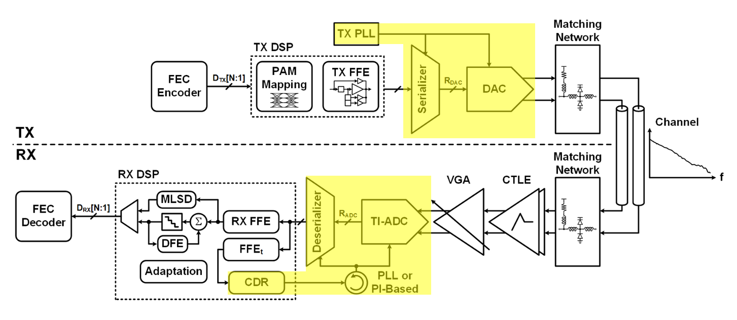 图01|原文配图(Silicon Co-Design)
As data speeds climb from 112Gbps to 224Gbps and 448Gbps, data starting running into physics constraint s and transceivers become more complex to compensate for these effects.
In this post I’ll be doing a system architecture breakdown of a modern DSP-based transceiver. I’ll explain the underlying physics constraints and the major blocks data passes through. Then, I’ll do a deep dive into the high-speed building blocks (shown in yellow) on the TX and RX side. I’ll be covering the following:
- The real problem: increasing data throughput under physical limits
- System Datapath overview
- 🔒TX Architecture: 🔒Serializer / Mux tree 🔒DAC - 6-7 Bit current steering DAC
- 🔒RX Side - Time-Interleaved ADC
- 🔒Clocking Architecture 🔒Clock Recovery: Bang Bang Phase Detector 🔒Clock Generation: LC-VCO Based PLL 🔒Multi-phase clock generation: The phase Interpolator 🔒Clock Distribution: Repeater, transmission line, and resonator-based
The real problem: increasing data throughput under physical limits
System Datapath overview
🔒TX Architecture:
- 🔒Serializer / Mux tree
- 🔒DAC - 6-7 Bit current steering DAC
🔒Serializer / Mux tree
🔒DAC - 6-7 Bit current steering DAC
🔒RX Side - Time-Interleaved ADC
🔒Clocking Architecture
- 🔒Clock Recovery: Bang Bang Phase Detector
- 🔒Clock Generation: LC-VCO Based PLL
- 🔒Multi-phase clock generation: The phase Interpolator
- 🔒Clock Distribution: Repeater, transmission line, and resonator-based
🔒Clock Recovery: Bang Bang Phase Detector
🔒Clock Generation: LC-VCO Based PLL
🔒Multi-phase clock generation: The phase Interpolator
🔒Clock Distribution: Repeater, transmission line, and resonator-based
Most of the figures in these slides are from the ISSCC tutorials as well as the papers in the references.
The real problem: increasing data throughput under physical limits
As data rates climb, we need to ask ourselves: what fundamentally constraints the data speed from first principles?
Data speed is now limited by physics and device parameters on the chip, which include, but not limited to, the following:
- Channel Loss: Loss scales with signal frequency, and high frequency attenuation rounds out the sharp edges of digital signals
- High impedance nodes in analog circuits: Active loads have a high input resistance, which is good for gain, but also creates dominant poles that lower overall BW.
- On-Chip Capacitance: Bigger transistors have bigger C that can affect rise/fall times of signals
- Noise / Jitter: The randomness in clock / data edges affect how fast those signals can be relative to the clock period. This impacts reliability of high speed digital circuits and time-interleaved switches
Channel Loss: Loss scales with signal frequency, and high frequency attenuation rounds out the sharp edges of digital signals
High impedance nodes in analog circuits: Active loads have a high input resistance, which is good for gain, but also creates dominant poles that lower overall BW.
On-Chip Capacitance: Bigger transistors have bigger C that can affect rise/fall times of signals
Noise / Jitter: The randomness in clock / data edges affect how fast those signals can be relative to the clock period. This impacts reliability of high speed digital circuits and time-interleaved switches
What tricks do designers have to increase speed? I contend there are two major paradigm shifts:
- Current steering circuits: These circuits steer constant currents through switches to a resistive load. The main advance is that it minimizes charging/discharging time of parasitic capacitors. However, current steering circuits tend to consume more power than equivalent charged-based topologies.
- Time interleaving: Instead of making a single component faster, place many in parallel and distribute data through “ranks” of S/H and T/H switches. Time interleaving introduces added complexity in clocks to coordinate parallel operations
Current steering circuits: These circuits steer constant currents through switches to a resistive load. The main advance is that it minimizes charging/discharging time of parasitic capacitors. However, current steering circuits tend to consume more power than equivalent charged-based topologies.
Time interleaving: Instead of making a single component faster, place many in parallel and distribute data through “ranks” of S/H and T/H switches. Time interleaving introduces added complexity in clocks to coordinate parallel operations
System Datapath overview
Next lets look at the major blocks in the datapath.
The function of a transceiver is quite simple: transmit a large amount of data from the TX and RX with minimal errors across a medium as fast as possible.
For short reach, low speed operation, the architecture relied mostly on analog blocks. However, due to recent data demands, one of the big paradigm shifts is a move to digital for the processing. Digital is great at performing parallel processing of data at a moderate clock (1-10’s GHz) frequency.
 图02|原文配图(Silicon Co-Design)
However, when it comes to data transmission, edge density becomes the constraint. You can only pack so much circuitry to drive the parallel channels on the edge of a chip and copper cables in the system.
As a result, data transmission favors serialized data at a high speed to pack as much data density as possible and transmit on a single cable.
These constraints influence the architecture of modern wireline transceivers.
On the TX Side, the main high speed blocks include:
- Forward Error Encoding (FEC) - Encodes the data with parity bits that correct for channel error at the RX side
- Feed Forward Equalization (FFE) - Pre-distorts the signal using a FIR filter to compensate for channel losses
- Serializer - Serializes the digital data from multiple channels and raises the effective output rate. 112 Gb/s PAM4 corresponds to a 56 GBd symbol rate, though practical serializers often use half-rate or quarter-rate architectures that are time-interleaved
- High-speed DAC - turns digital symbols into an analog waveform
- Driver - amplitudes the signal before it is transmitted on the channel
Forward Error Encoding (FEC) - Encodes the data with parity bits that correct for channel error at the RX side
Feed Forward Equalization (FFE) - Pre-distorts the signal using a FIR filter to compensate for channel losses
Serializer - Serializes the digital data from multiple channels and raises the effective output rate. 112 Gb/s PAM4 corresponds to a 56 GBd symbol rate, though practical serializers often use half-rate or quarter-rate architectures that are time-interleaved
High-speed DAC - turns digital symbols into an analog waveform
Driver - amplitudes the signal before it is transmitted on the channel
In the Channel:
- Matching network - matches the TX and RX to the characteristic impedance to avoid reflections and transmission line effects
- Channel - attenuates and distorts the transmitted signal
Matching network - matches the TX and RX to the characteristic impedance to avoid reflections and transmission line effects
Channel - attenuates and distorts the transmitted signal
In the RX:
- Receiver front-end - conditions the signal by amplifying it (variable gain amplifier) and providing equalization (CTLE)
- TI-ADC - converts the analog value to digital values
- Deserializer - converts the digitized data from the transmission rate to the digital frequency
- DSP - processes and recovers data
Receiver front-end - conditions the signal by amplifying it (variable gain amplifier) and providing equalization (CTLE)
TI-ADC - converts the analog value to digital values
Deserializer - converts the digitized data from the transmission rate to the digital frequency
DSP - processes and recovers data
As a result of the added digital complexity, high speed and parallel processing blocks require a robust clock architecture to synchronize the data properly.
In the following sections, we’ll step through each of the high speed blocks, with the principle of operation, the key impairments, and how they affect the system level.
TX Architecture
After the paywall I’ll dive right into the TX architecture. Check out my other posts as well:
第二部分:解析(深度解读)
以下为基于原文的结构化中文解读,仅供学习交流,不代表原作者观点。
一、这篇文章在讲什么
Silicon Co-Design 这篇(标题含 “Pushing the Speed Limit: Designing SerDes Transceivers for the 224 and 448Gbps Scaling Era”)聚焦 224/448 Gbps SerDes 收发器的系统级架构拆解。文章把 SerDes 从「一颗 PHY」放回「整个 AI 机架互连」的背景里:随着 Scale-up 域带宽需求爆炸,单通道速率从 112G 走向 224G、再探 448G,PHY 架构、均衡、时钟、封装与信道建模必须一起重新设计。
二、关键概念拆解
- 速率阶梯 112→224→448 Gbps:每代翻倍的背后是 PAM4 阶数、符号率与 DSP 复杂度的同步膨胀。
- 发射/接收均衡:FFE、CTLE、DFE 与判决反馈在更高符号率下裕度收窄,功耗与面积压力陡增。
- 时钟与抖动:448G 对参考时钟抖动、PLL 噪声的要求进入亚皮秒级,CDR 设计变难。
- 封装与信道:封装内走线、连接器、背板的损耗/串扰成为「能否跑通 448G」的物理前提,先进封装与材料是关键。
- 系统级视角:SerDes 不只是 PHY IP,而是和拓扑、路由、集合通信库耦合的端到端问题。
三、与本站其他文章的衔接
- CPO / 光互联系列:当电 SerDes 在 448G 撞墙,正是 CPO、硅光收发器、DWDM 微环登场的根本驱动力——电互连在「带宽×距离×功耗」三角上吃紧。
- SerDes 系列(本站已有 Part 1/2):本文是 224/448G 速率前沿的专题补全。
- AI 机架 Scale-up 系列:SerDes 是 Scale-up 域最底层的物理链路,其上才是网络拓扑与协同设计。
四、趋势与投资映射
- 价值从「交换芯片」下沉到「高速 SerDes PHY IP + 先进封装 + 低损耗材料/连接器」;448G 能否量产决定 CPO 的时间表。
- 风险:448G 电链路功耗/信道裕度极紧,若迟迟无法商用,行业会更激进地跳向光(CPO/线性直驱光模块),反过来压制传统 SerDes 估值。