SerDes 技术全景(上篇):读懂 CPO 之前必须掌握的电侧互连底座
对硅谷模拟 IC 设计工程师 Nutty 的 SerDes 技术科普(系列第一篇)的英文原文与中文解读。从并串转换的物理动机、PAM4 调制、DAC/ADC SerDes,到铜的物理极限与 CPO/LPO/光 DSP 的承接关系,讲清为什么「数字时代反而最缺模拟设计」。全文公开无付费墙。
原文:Nutty(Substack,handle: nuttycld,硅谷模拟 IC 设计工程师),发布于 2026-08-05。 本文为「英文原文 + 中文深度解读」对照版。作者文末声明不构成投资建议,且可能持有文中提及公司的证券。 译注:本译文发布于 2026-08-07;原文为系列第一篇(Part 1),Part 2 将转向「技术与资金流向」的公司分析。
第一部分:正文(Original Article)
[Public] SerDes Part 1: The Technology You Should Know Before CPO
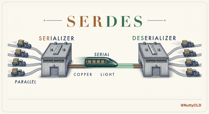 Figure. Cover — SerDes sits at the heart of the interconnection era.
An analysis of industry and technology structure, not investment advice · The author may hold positions in securities mentioned
I work in Silicon Valley as an analog IC design engineer. Lately my LinkedIn inbox has been filling up with messages like the one below, all about SerDes (Serializer and Deserializer) engineer positions.
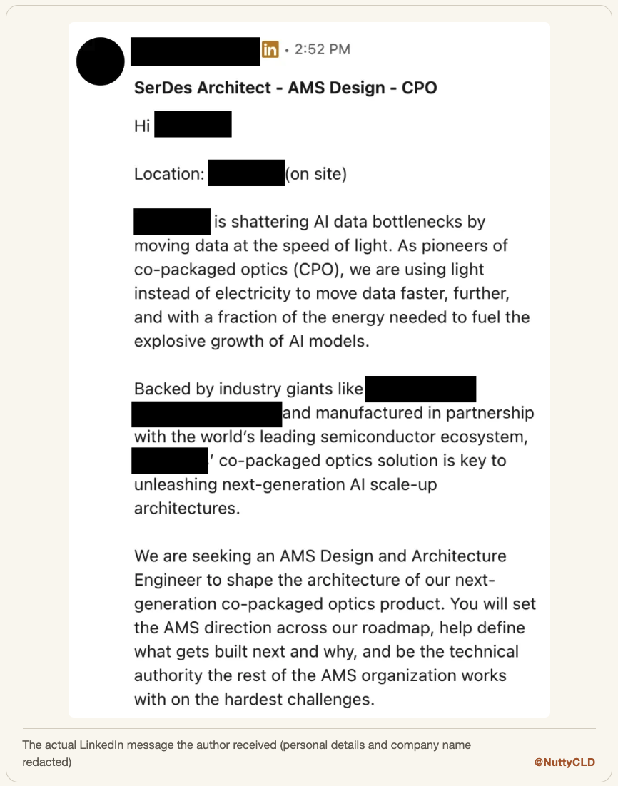 Figure. A typical recruiter outreach — a CPO company is desperately hunting for analog SerDes designers.
Most of you are probably familiar with CPO, but I suspect SerDes (Serializer-and-Deserializer) is new to many. Today I want to walk through just how deeply this technology is embedded in the current interconnection era. For the record, the message below came from a recruiter at one of the companies that will appear in this article. In the age of CPO, the emblem of the digital and optical era, the person this company is desperately hunting for is, ironically, an analog designer.
I Know Analog and Digital
We lived through the age of analog communication and now live in a thoroughly digital one. As with computing, communication is a field digital has won outright. The reason is the noise tolerance of digital signals. By the nature of communication, data is attenuated as it crosses a transmission line and distorted by outside factors. Since delivering data exactly as sent is the highest virtue in communication, these factors are weeds: things to be removed or suppressed by any means available. In an analog signal, every level carries meaning, so faithfully reconstructing the transmitted level at the receiver is tricky. Digital only has to tell 0 from 1, so even with some noise mixed in, recovery is comparatively easy. Which is why communication has always been digital, and always will be.
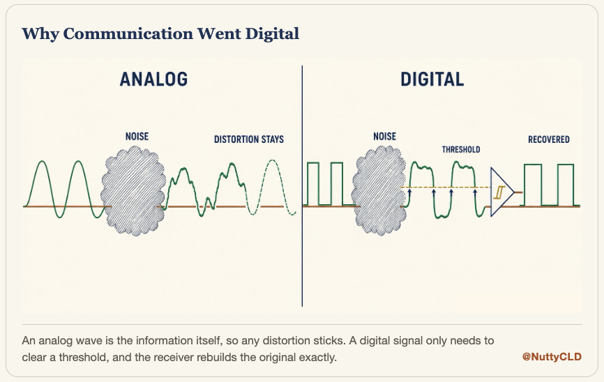 Figure. Why digital won communication: it only needs to tell 0 from 1.
But as AI training and inference put ever more GPUs, CPUs, and memory to work, and the volume of data to move kept climbing, digital communication began running into limits. You know HBM: High-Bandwidth Memory, that is, memory with large bandwidth. Conceptually, you can read bandwidth here as the number of transmission lines. In other words, it solves the problem of moving lots of data by sending it in parallel over many lines. But not every application can raise bandwidth through this kind of parallelization, because laying more lines is itself a cost. The next idea, then, is to serialize the data and send it fast. And that is exactly what a SerDes circuit does.
Now I Know SerDes as Well
What a SerDes (Serializer and Deserializer) does is the same whether the link is electrical or optical. That is a question about the material of the transmission line, and has nothing to do with the methodology of sending more data faster. So SerDes has existed from the early days until now, and will keep existing even after optical links become the norm inside a rack. That does not mean it sits outside today’s datacenter communication revolution. On the contrary, its importance keeps rising. The biggest reason of all: the amount of data the AI industry creates and moves has exploded.
Inside a chip, data travels in parallel along thousands, tens of thousands of wires. The trouble starts the moment it has to leave the chip. To build transmission lines matched to that data volume, the number of physical wires would have to grow with it. Look inside a datacenter linking tens of thousands of GPUs, or a rack inside one, and the wires and optical cables are already packed about as tight as they could possibly be.
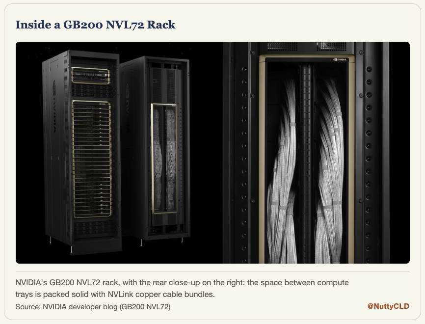 Figure. Wires and optical cables inside a rack are already packed as tight as physically possible.
If we tried to send data off-chip in parallel, the wires and optical cables would end up occupying more volume than the chips themselves. Physically and economically, that is not a viable path.
So at the chip boundary, where transmission begins, a special circuit is attached. It serializes the parallel data on the way out (transmit side), or parallelizes the serial data on the way in (receive side). The Serializer does the former, the Deserializer the latter. As in the picture below, think of goods carried by many trucks being loaded onto one very fast express train, then split back across many trucks on the receiving end.
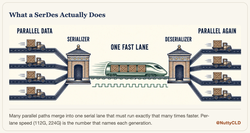 Figure. SerDes in one picture: parallel trucks consolidated onto one fast serial train.
Naturally, the serialized data has to move faster than the parallel data did. If ten trucks each deliver one package per second, the train must carry ten packages per second to avoid a bottleneck. It has to run ten times faster. The numbers the industry throws around, 112G and 224G, mean exactly this transfer speed. One lane, meaning one path the data travels along, carrying 112 billion bits per second, is what we call 112G/lane. The industry is now crossing over to 224G/lane, and the next generation, 448G/lane, is under continuous development.
How far this speed can be pushed is one of the key technical metrics of a SerDes. Of course cost cannot be ignored, and here the cost is power. So the metric that matters most is how fast you can carry data within a limited power budget. Improving that metric is what circuit designers like me stay up all night wrestling with. To add one number for a sense of scale: by an NVIDIA ($NVDA) estimate, in the same 100K-server-class datacenter, the transceivers (optical modules) draw 2.3 MW in a traditional cloud and 40 MW in an AI factory. The electricity spent just carrying data now rivals a decent-sized power plant.
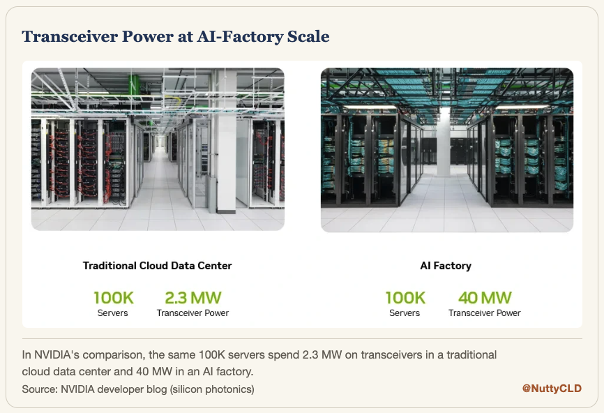 Figure. Transceiver power scales from 2.3 MW (cloud) to 40 MW (AI factory) — data movement now rivals a power plant.
NVIDIA’s fiscal 2026 annual report shows computing chip revenue up 59%, while revenue from networking, the business of connecting those chips, grew 142%. These numbers are proof of why this is the age of communication, and of how much this technology matters.
The Age of Interconnection
Apr 22
PAM4? I Think I’ve Heard That Somewhere
If you follow this field a bit more closely, you have probably run into the term PAM4 (Pulse Amplitude Modulation, 4-level). The digital communication we usually think of uses NRZ (Non-Return-to-Zero); there is also RZ, Return-to-Zero, which I will skip here. As the figure below shows, NRZ is a signaling scheme with two levels, 0 and 1, PAM4 with four, and PAM6 with six.
More bits per level (NRZ carries 1 bit; PAM4 carries 2) means more information loaded onto each carrier. To send the pattern 01, NRZ has to transmit twice, a 0 and then a 1, while PAM4 sends one symbol at the level that means 01 and delivers the same information in one shot. Think of it as raising the payload per shipment. Obviously favorable for moving data. Today’s 112G and 224G links all use PAM4.
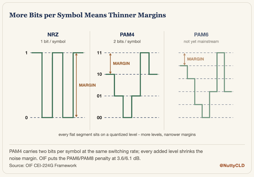 Figure. NRZ (2 levels), PAM4 (4 levels), PAM6 (6 levels) — more levels, more bits per symbol.
So why not PAM6 or PAM8? A perfectly sensible question. And it is true that the bigger the number, the more favorable the transmission becomes. But this is where we need to recall the history of analog signals ceding their place in communication to digital.
As you may have noticed, this is digital taking a step back toward analog. The most important line dividing analog from digital is the continuity of levels, so the more levels you slice the transmission into, the more analog-like the communication becomes. And that makes it vulnerable to exactly the attenuation and distortion we discussed earlier. In the figure above, you can see the width of the bands marked ‘margin’ shrink as the PAM number grows. Within that margin, a certain amount of distortion can be recovered at the receiver, but as the margin narrows, the allowance for recoverable attenuation and distortion shrinks with it. Pile on levels recklessly and the receiver can no longer tell them apart, which wrecks the essential purpose of communication: sending and receiving data accurately.
The standards body OIF calculates that, holding the same error rate, PAM6 requires 3.6 dB more noise margin than PAM4, and PAM8 requires 6.1 dB more. PAM8 needs 4x the SNR (Signal-to-Noise Ratio) of PAM4. To get there you either double the signal or halve the noise. Boosting the signal means raising the voltage, which burns additional power, and noise has physical floors that make it even harder to reduce. Even so, the industry keeps probing PAM6 for the next generation, 448G, and ISSCC, the field’s flagship conference, publishes research on higher level counts every year. It is a door that will have to be passed through someday, so people keep knocking.
Now I Understand Why Analog Design Matters
Now the recruiter messages from the opening make sense. Why, in the age of digital, in a field digital has conquered, analog designers of all people are becoming so necessary.
The circuit that gathers data and converts it into a multi-level signal like PAM4 is the Serializer; to add technical precision, a DAC (Digital-to-Analog Converter)-based Serializer. The receive side, in turn, is called an ADC (Analog-to-Digital Converter)-based Deserializer. These data converters are among the main IPs that keep many analog designers fed. Not that digital designers are going hungry; on the contrary, their side keeps gaining importance too. Analog designers focus strictly on the conversion. The converted digital signals then run complex algorithms back in the digital world. The flagship example: at the receiver, digital algorithms strip out the distortion and attenuation picked up along the way and reconstruct the original signal. And that work is genuinely expensive. It is not rare for the receive-side DSP to consume more than 50% of the link’s total power.
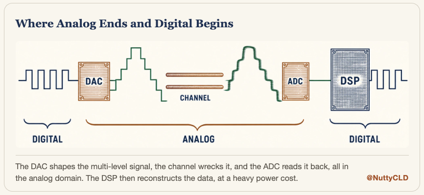 Figure. The Serializer is DAC-based; the Deserializer is ADC-based.
Still, the bottleneck remains the analog circuitry. Ever-climbing speeds, circuit noise, the non-ideal behavior of transmission lines, jitter in the clocks driving the data converters: the problems that have tormented analog designers all along keep escalating in difficulty, making the design ever harder.
Analog’s troubles do not end there; they spread beyond the chip. The public datasheet for Panasonic’s Megtron 6, a material widely used in high-speed boards, specifies material properties only up to 10GHz, because beyond that you are in RF (Radio Frequency) territory, where complicated frequency behavior starts to matter. Yet the fundamental frequency of a 224G signal already sits near 56GHz. Once a signal’s fundamental crosses 50GHz, every trace, via, and connector contact in the package and board starts acting like an antenna and a filter that distorts the signal. In short, from 224G on, ‘a good circuit, a good SerDes IP’ is not enough. Chip, package, and board have to be designed together as one system, and the gap between teams that have done this and teams that have not is stark.
So as demand for high-speed communication grows, analog design has become a core technology again, and companies are out pounding the pavement for those designers. Look closely at this job market, though, and one feature jumps out. On the career boards of NVIDIA, Marvell ($MRVL), Intel ($INTC), Cadence ($CDNS), and the like, the SerDes and analog postings are almost entirely Senior, Staff, and Principal; the ranks below are rare. It is a market with no time to train juniors and wait, where companies poach seasoned designers from one another. This leads to outcomes like Qualcomm ($QCOM) acquiring the SerDes IP company Alphawave. Buy the company, restock the roster overnight.
Okay, I Understand SerDes Is a Sophisticated Technology, but Why Should I Know This?
Time to bring up optical communication again, the topic that set the market on fire this year.
An Investor’s Handbook I - AI Optics
That copper keeps losing territory to optics is self-evident. Yet copper is still in use, and will remain so. Which is why it matters to know how far copper can physically go. Copper attenuates a signal more as frequency rises. The copper-cable reach objectives OIF has set by speed generation run about 2 m at 112G and 1 m at 224G. A server rack today stands 2 m tall, so at just 224G, spanning even a single rack on copper alone becomes difficult. Distance is not the only problem. By OIF’s system power targets, the energy to send one bit is about 0.7 pJ inside a package (a few cm) but climbs steeply to about 3.5 pJ over a board path of about 1 m.
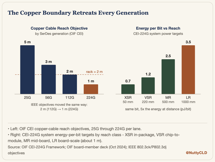 Figure. Copper reach shrinks to ~1 m at 224G; per-bit energy climbs from 0.7 pJ (in-package) to 3.5 pJ (1 m board).
The generational shift in optical modules we all know is the result of light filling the ground that copper has surrendered. It runs from pluggables in the equipment faceplate, to LPO with the module DSP removed, to CPO, the hottest topic of the moment, with the optics attached right beside the switch chip. Light keeps replacing copper and moving toward the chip.
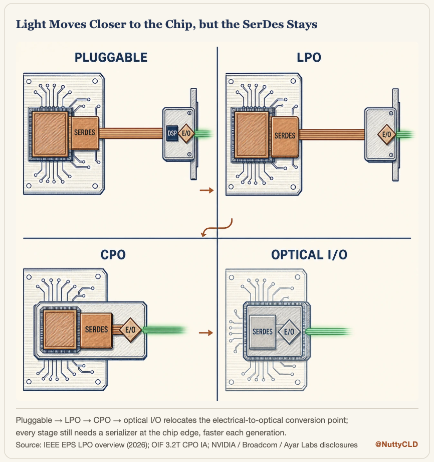 Figure. The optical module generations: pluggable → LPO → CPO.
If you have followed along this far, you can now spot at a glance, in each of those diagrams, the SerDes circuit and the electrical-optical converter that never leave the picture. Whichever generation the optical module belongs to, those two do not disappear. However far audio equipment advances, microphones and speakers do not go away.
LPO removed the DSP to cut power consumption, and handed the duty of signal recovery to the SerDes. The recovery here is not about distortion inside the optical fiber; it is about distortion arising on the electrical stretch leading to the optical module. Fiber has almost no loss at these distances. The problem is the 20 cm or so of copper running across the board from the switch chip to the faceplate module, and CPO shrinks that stretch to millimeters by attaching the optical engine right next to the chip. With fewer problems arising, a simple DSP implemented inside the SerDes can stand in for the heavy module-side DSP. Per NVIDIA’s materials, of the 30W that one pluggable draws, 20W is the module DSP’s share, while CPO does the same job in 9W.
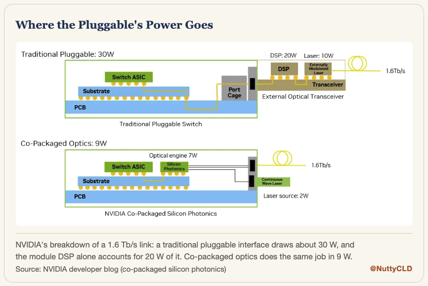 Figure. Of a pluggable’s 30W, ~20W is module DSP; CPO does the same job in 9W.
The chip the industry calls an ‘optical DSP’ is the DSP that sits inside an optical module and restores the electrical signal on both sides of the electrical-optical conversion. Beyond reviving the electrical signal that arrived at the module, it also corrects the distortion created by the bandwidth limits of the laser, the modulator, and the receiving devices. It is ultimately the same family of technology as the DSP inside a host SerDes, and that is why the companies that are good at SerDes become the stars of the optical DSP market.
A SerDes must sit at both ends of the link whether the transmission medium is electrical or optical, so it will remain in place even when optical communication becomes mainstream. DSP is a little different. The DSP that has moved inside the SerDes will still be needed, but the DSP inside the optical module that corrects signal distortion from the chip-to-module path is likely to disappear as that path grows shorter. When you look at the companies in this space, you can only forecast properly by matching what each company actually focuses on to the future expected for that focus.
NVIDIA’s published spec for its 102.4-terabit-class CPO switch explicitly lists 512 lanes. The high-speed electrical lanes did not disappear; they only moved from outside the package to inside. The standard-bearer of the farthest-out camp, optical I/O, is Ayar Labs, which introduces its product TeraPHY as ‘a retimer that cleans up the electrical signal and hands it over to the optical link.’ A retimer takes a signal weakened along the way, restores it to a clean state, and sends it on: a role much like an EV charging station on a long route. To do this, a SerDes circuit has to go inside the retimer. In effect, Ayar Labs has put forward ‘the SerDes in front of the optical link’ as its flagship product.
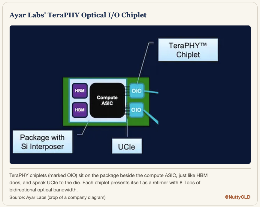 Figure. Ayar Labs frames TeraPHY as ‘the SerDes in front of the optical link.’
A sharp reader will surely ask this question:
An optical fiber can carry several beams of light at different wavelengths on a single strand (wavelength-division multiplexing, WDM), so why bother serializing at all?
A fair point, and that is exactly what the industry does. The next-generation IEEE standard specifies 800 gigabits carried on four wavelengths over a single fiber. But what each of those four wavelengths carries is data serialized at the 224G class (200 billion bits per second) we saw earlier. The approach is not ‘stop using SerDes’; it is ‘multiply the SerDes lanes here.’ In this respect, fiber is undeniably attractive. But physical constraints exist here too. WDM does not come free. Parallelizing light means adding an entire set of laser, modulator, and receiver components for every wavelength, and that, too, is a cost. The next-generation spec stopping at four wavelengths is a compromise struck around exactly this cost (come to think of it, the number 4 seems to have something magical about it. PAM4, too..).
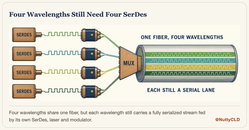 Figure. WDM runs multiple wavelengths over one fiber — but each wavelength still carries 224G-class serialized data.
So, Should I Just Buy the Best SerDes Company?
Whichever architecture wins, demand for high-speed electrical design skill is not going away; that much is now well understood. That is the technology side of the story. As investors, we arrive at the one-dimensional conclusion: “Fine, then I should invest in the companies that are good at SerDes.” Unfortunately, companies that make money by putting this IP front and center are hard to find. If today is the first time you have encountered this term, that in itself is evidence of the technology’s low visibility. Take cars as an analogy: the engine is the heart of the car, but companies that made big money selling pure ‘engine blueprints’ are rare. The big money is made on the finished car that carries the engine (with EVs as the exception, of course).
We need to sharpen the question beyond ‘who is best at SerDes.’ ‘Who is converting SerDes skill into money, and how: in systems, in products, in components?’ In Part 2, I will connect the flow of technology to the flow of money. We will look at how 13 key companies put this skill to work from the component, product, and system angles, and we will also look at one more inventive use of it, perhaps the most valuable one of all.
Key Sources
- Standards and industry documents: OIF (copper reach and power targets, PAM signal analysis), IEEE 802.3 (next-generation optical specifications)
- Company technical materials: NVIDIA (datacenter power, CPO switch specifications), Ayar Labs, Panasonic (board material datasheet)
- Job postings: NVIDIA, Marvell, Intel, and Cadence career boards (viewed 2026-08)
- Press releases and filings: Qualcomm (Alphawave acquisition)
Disclaimer: This article is intended as a reference for understanding the industry and its underlying technology and was not written as investment advice. The figures and information used in this article are based on publicly available materials. The author may hold shares in companies mentioned in the article. All investment decisions and their outcomes are the reader’s own responsibility.
第二部分:解析(深度解读)
核心论点摘要
硅谷模拟 IC 设计工程师 Nutty 用一篇面向「非专业投资者」的科普,讲清了一个反直觉的事实:在人人高喊「数字时代、AI 算力」的今天,最稀缺的反而是一群模拟电路设计师——因为把数据搬出家门的那段「电侧互连」,本质上是模拟问题。
文章主线:
- 数字通信靠「容噪」赢了模拟,但 AI 把数据量推到并行布线承载不住 → 必须串行化(SerDes)提速;
- 速度从 112G/lane → 224G/lane → 448G/lane,功率是核心约束;
- 为在有限功率内塞更多比特,行业用 PAM4(每符号 2 bit),但 PAM 阶数越高越「像模拟」、越怕衰减失真,PAM6/8 收益递减;
- 把并行数据变成 PAM4 多电平信号的是 DAC-based Serializer,接收端是 ADC-based Deserializer;接收端 DSP 吃掉链路 >50% 功耗,但瓶颈仍在模拟电路与「芯片-封装-板」协同设计;
- 铜在 224G 已逼近物理极限(单机架 2 m 高,铜只能走 ~1 m),于是光接替铜、从可插拔 → LPO → CPO 一路逼近芯片;但 SerDes 与电光转换器永不消失;
- CPO 把光引擎贴到交换芯片旁,把「芯片到模块那 20 cm 铜」缩到毫米,于是模块侧重型 DSP 可被 SerDes 内部轻量 DSP 取代(30W 可插拔 → 9W CPO);
- 投资视角:SerDes 是「发动机」,但靠卖纯 SerDes IP 赚大钱的公司很少,要问的是「谁把 SerDes 能力转化成了系统/产品/器件上的钱」——Part 2 将拆解 13 家公司。
关键概念解读
- SerDes(串行器/解串器):在芯片边界把并行数据串行化发出、或把串行数据并行化解出。链路是电是光不影响其职责——所以它既不会因光互连普及而消失,也不会因 CPO 而被取代。
- 112G / 224G / 448G(per lane):单条通道的传输速率。十辆卡车各 1 包/秒,火车就得 10 包/秒、跑十倍快——这就是「串行提速」的物理直觉。
- PAM4(4 电平脉冲幅度调制):NRZ 每符号 1 bit,PAM4 每符号 2 bit,等效「每趟多载货」。但阶数越高越接近模拟、容噪裕度(margin)越窄;OIF 测算 PAM6 比 PAM4 多要 3.6 dB 噪声裕度、PAM8 多 6.1 dB(=4× SNR)。
- DAC-based Serializer / ADC-based Deserializer:发送端用 DAC 把数字并行数据合成多电平模拟信号;接收端用 ADC 采样还原。数据转换器是模拟设计师的核心 IP。
- 接收端 DSP(数字信号处理):在数字域用算法剥离沿路衰减/失真、重建原信号,常占链路 >50% 功耗——但瓶颈仍在模拟前端。
- LPO(Linear Pluggable Optics)与 CPO(Co-Packaged Optics):LPO 拔掉模块 DSP 省电,把信号恢复甩给 SerDes;CPO 把光引擎贴到交换芯片旁,把芯片到模块那截铜从 20 cm 缩到毫米,模块侧 20W DSP 被 SerDes 内轻量 DSP 取代(NVIDIA:可插拔 30W,其中 20W 是模块 DSP;CPO 9W 干同样的活)。
- 光 DSP vs 主机 SerDes DSP:光模块里的「光 DSP」纠正电光转换两侧的电信号、并补偿激光器/调制器/探测器的带宽失真——与主机 SerDes 内 DSP 同宗同源,所以「擅长 SerDes 的公司」天然是光 DSP 市场的明星。
- Retimer(重定时器):把沿途衰弱的信号复原干净再送出,像长途上的充电站。Ayar Labs 把 TeraPHY 定义为「光链路前的 SerDes」——光 I/O 的旗帜产品。
- WDM(波分复用):一根光纤跑多波长,但每个波长仍承载 224G 级串行数据——不是「不用 SerDes」,而是「在这里把 SerDes 车道翻倍」。下一代 IEEE 标准一根光纤 4 波长传 800G,停在 4 波长是成本妥协。
技术拐点与产业含义
- 56GHz 是分水岭:224G 信号基频已近 56GHz,越过 50GHz 后封装/板上的每一条走线、过孔、连接器都开始像天线和滤波器一样扭曲信号——「好电路 + 好 SerDes IP」不够了,必须芯片-封装-板协同设计。
- 模拟人才稀缺且不可速成:NVIDIA / Marvell / Intel / Cadence 的 SerDes 岗几乎全是 Senior/Staff/Principal,鲜有初级——公司等不起培养周期,只能互相挖角(如 Qualcomm 收购 Alphawave 一夜补齐阵容)。
- 铜极限是 CPO 的需求源头:224G 铜只能走 ~1 m(机架高 2 m),单机架内用铜都困难;每比特能耗从封装内 0.7 pJ 涨到 1 m 板级 3.5 pJ。光填铜让出的地盘,正是 CPO 叙事的土壤。
- SerDes 是贯穿所有光模块的常量:无论可插拔 / LPO / CPO,SerDes + 电光转换器都在;差别只在「模块侧 DSP 去了哪里」——路径越短,模块侧 DSP 越可能被 SerDes 内 DSP 取代。
- NVIDIA 102.4T CPO 交换芯片明示 512 条 lane:高速电通道没消失,只是从封装外搬进了封装内。
与本站其他文章的连接
- 本篇是 CPO 系列在「电侧」的技术底座:本站的 Pushing the Speed Limit:224/448Gbps 时代的 SerDes 收发器架构拆解 讲 SerDes 收发器的系统架构与功耗墙,本篇从「为什么需要 SerDes、PAM4 与模拟设计的不可替代性」补上更底层的动机。
- 光侧器件供货方见 Sivers Semiconductors:一只被市场忽视的 $130M 市值 CPO / LiDAR / SATCOM 标的——CPO 把激光器移到封装外(ELS/ELSFP),Sivers 的 InP DFB 激光阵列正是这条故事的供给侧答案。
- 系统/生态视角见本站 CPO 专题(CPO Fully Dissected、There Is No Such Thing As A CPO Stock、CPO Biggest Bottleneck: High Volume Testing)。
- 本篇 Part 2 将拆解 13 家公司的「SerDes 能力→收入」转化路径,可与本系列互文阅读。
风险提示
- 本文为技术科普 + 投资视角的英文译文与解读,不构成投资建议;原作者为硅谷模拟 IC 工程师,可能持有文中公司(NVIDIA、Marvell、Intel、Cadence、Qualcomm 等)证券。
- 技术路线仍有变数:PAM6/8 能否在 448G 落地、各代光模块(LPO/CPO)渗透率与时间表、WDM 波长数妥协,均受功耗、良率与成本牵制。
- 投资层面(作者预告的 Part 2 主题):「擅长 SerDes」不等于「能靠 SerDes IP 赚大钱」,需区分公司在系统 / 产品 / 器件三层的变现路径,警惕把技术热度直接等同于标的收益。
- 英文原文图表版权归原作者 Nutty 及 OIF / NVIDIA / Panasonic / Ayar Labs / IEEE 等各自所有,引用已标注来源。