Pushing the Speed Limit:224/448Gbps 时代的 SerDes 收发器架构拆解
对 Chad(Inside the Silicon Machine)关于 224/448Gbps SerDes 收发器的系统架构拆解的英文原文与中文深度解读,覆盖 DSP 数据通路、电流舵 DAC、时间交织 ADC 及时钟架构的物理约束。⚠️ 原文含付费墙,时钟细节未含。
原文:Chad,Inside the Silicon Machine(Substack),发布于 2026-03-23。 本文为「英文原文 + 中文深度解读」对照版。 ⚠️ 付费墙说明:原文在 Clocking Architecture(时钟架构)章节引言后即进入付费内容——时钟恢复(Bang-Bang 相位检测器)、时钟生成(LC-VCO PLL)、多相时钟(相位插值器 PI)、时钟分配(中继/传输线/谐振器)均为付费细节。「第二部分·解读」仅基于免费公开部分展开,未含付费深解,不实装付费内容。
第一部分:正文(Original Article)
Pushing the Speed Limit: Designing SerDes Transceivers for the 224 and 448Gbps Scaling Era
An architectural analysis of DSP-driven SerDes datapaths, current-steering nonidealities, and the multi-phase clock constraints breaking modern wireline links.
By Chad
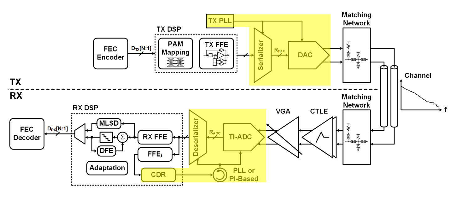 Figure 1. DSP-Based Transceiver architecture. Reproduced from A. Carusone et al., ‘Modern Wireline Transceivers,’ IEEE Journal of Solid-State Circuits, vol. 61, no. 2, pp. 395–422, Feb. 2026, licensed under CC BY-NC-ND 4.0.
As data speeds climb from 112Gbps to 224Gbps and 448Gbps, data starting running into physics constraints and transceivers become more complex to compensate for these effects.
In this post I’ll be doing a system architecture breakdown of a modern DSP-based transceiver. I’ll explain the underlying physics constraints and the major blocks data passes through. Then, I’ll do a deep dive into the high-speed building blocks (shown in yellow) on the TX and RX side. I’ll be covering the following:
- The real problem: increasing data throughput under physical limits
- System Datapath overview
- TX Architecture:
- Serializer / Mux tree
- DAC - 6-7 Bit current steering DAC
- RX Side - Time-Interleaved ADC
- 🔒Clocking Architecture
- 🔒Clock Recovery: Bang Bang Phase Detector
- 🔒Clock Generation: LC-VCO Based PLL
- 🔒Multi-phase clock generation: The phase Interpolator
- 🔒Clock Distribution: Repeater, transmission line, and resonator-based
Most of the figures in these slides are from the ISSCC tutorials as well as the papers in the references.
The real problem: increasing data throughput under physical limits
As data rates climb, we need to ask ourselves: what fundamentally constraints the data speed from first principles?
Data speed is now limited by physics and device parameters on the chip, which include, but not limited to, the following:
- Channel Loss: Loss scales with signal frequency, and high frequency attenuation rounds out the sharp edges of digital signals
- High impedance nodes in analog circuits: Active loads have a high input resistance, which is good for gain, but also creates dominant poles that lower overall BW.
- On-Chip Capacitance: Bigger transistors have bigger C that can affect rise/fall times of signals
- Noise / Jitter: The randomness in clock / data edges affect how fast those signals can be relative to the clock period. This impacts reliability of high speed digital circuits and time-interleaved switches
What tricks do designers have to increase speed? I contend there are two major paradigm shifts:
- Current steering circuits: These circuits steer constant currents through switches to a resistive load. The main advance is that it minimizes charging/discharging time of parasitic capacitors. However, current steering circuits tend to consume more power than equivalent charged-based topologies.
- Time interleaving: Instead of making a single component faster, place many in parallel and distribute data through “ranks” of S/H and T/H switches. Time interleaving introduces added complexity in clocks to coordinate parallel operations
System Datapath overview
Next lets look at the major blocks in the datapath.
The function of a transceiver is quite simple: transmit a large amount of data from the TX and RX with minimal errors across a medium as fast as possible.
For short reach, low speed operation, the architecture relied mostly on analog blocks. However, due to recent data demands, one of the big paradigm shifts is a move to digital for the processing. Digital is great at performing parallel processing of data at a moderate clock (1-10’s GHz) frequency.
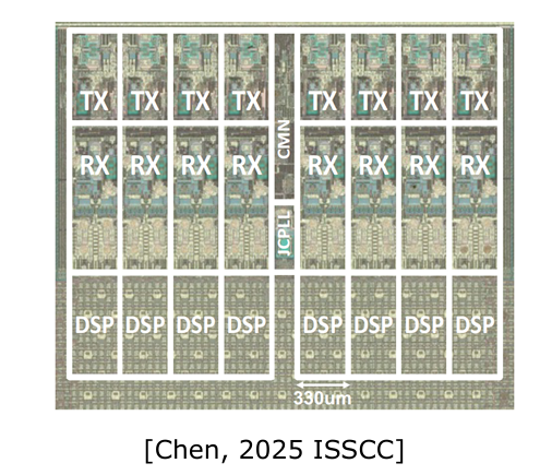 Figure 2. A 224Gbps PAM-4 8-Lane Serdes for backplane interconnect. Source: W. Chen, “Clocking and CDR Techniques for High Performance Wireline Transceiver” presented at the IEEE International Solid-State Circuits Conf. (ISSCC), San Francisco, CA, Feb. 15-19, 2026.
However, when it comes to data transmission, edge density becomes the constraint. You can only pack so much circuitry to drive the parallel channels on the edge of a chip and copper cables in the system.
As a result, data transmission favors serialized data at a high speed to pack as much data density as possible and transmit on a single cable.
These constraints influence the architecture of modern wireline transceivers.
On the TX Side, the main high speed blocks include:
- Forward Error Encoding (FEC) - Encodes the data with parity bits that correct for channel error at the RX side
- Feed Forward Equalization (FFE) - Pre-distorts the signal using a FIR filter to compensate for channel losses
- Serializer - Serializes the digital data from multiple channels and raises the effective output rate. 112 Gb/s PAM4 corresponds to a 56 GBd symbol rate, though practical serializers often use half-rate or quarter-rate architectures that are time-interleaved
- High-speed DAC - turns digital symbols into an analog waveform
- Driver - amplitudes the signal before it is transmitted on the channel
In the Channel:
- Matching network - matches the TX and RX to the characteristic impedance to avoid reflections and transmission line effects
- Channel - attenuates and distorts the transmitted signal
In the RX:
- Receiver front-end - conditions the signal by amplifying it (variable gain amplifier) and providing equalization (CTLE)
- TI-ADC - converts the analog value to digital values
- Deserializer - converts the digitized data from the transmission rate to the digital frequency
- DSP - processes and recovers data
As a result of the added digital complexity, high speed and parallel processing blocks require a robust clock architecture to synchronize the data properly.
In the following sections, we’ll step through each of the high speed blocks, with the principle of operation, the key impairments, and how they affect the system level.
TX Architecture
Serializer / Mux tree
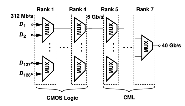 Figure 3. A Binary-Mux Tree. Reproduced from B. Razavi, “Design Techniques for High-Speed Wireline Transmitters,” IEEE OJ-SSCS, 2021 (CC BY).
The mux tree is used for serializing / deserializing data. Here, stages of 2-1 muxes are arranged in ranks. This ensure each interconnect between muxes aren’t heavily loaded that can slow down operation.
The final rank operates with the highest-rate clock, while earlier ranks use divided versions of that clock so that each stage runs at a rate compatible with its local data rate.
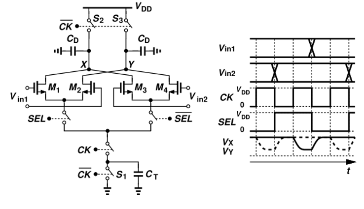 Figure 4. A Basic charge-steering MUX. Reproduced from B. Razavi, “Design Techniques for High-Speed Wireline Transmitters,” IEEE OJ-SSCS, 2021 (CC BY).
A common high-speed mux cell is the current steering mux cell. This cell uses two differential pairs for each of the inputs. To select each input, the SEL signal, synchronized to the CLK, steers the current between the two input branches.
Impairments
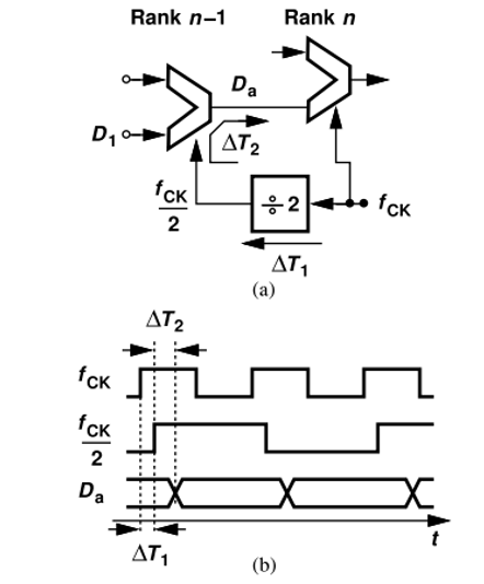 Figure 5. Divider and MUX Delay. Reproduced from B. Razavi, “Design Techniques for High-Speed Wireline Transmitters,” IEEE OJ-SSCS, 2021 (CC BY).
- Kickback noise from clock feedthrough. Clock feedthrough and switching transients can disturb internal common-mode nodes and degrade timing margin, especially in the final high-speed stages.
- Skew between SEL and clk.
- Skew between stages in the MUX tree. The accumulated clock delay associated with the driver and the mux itself can cause ranks to fail to clock the data fast enough.
DAC - 6-7 Bit current steering DAC
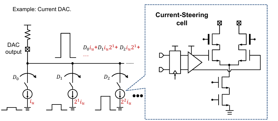 Figure 6. Ideal DAC with Current steering cell. Source: S. Su, “Principles and Practices of High-Speed Digital-to-Analog Converter Design” presented at the IEEE International Solid-State Circuits Conf. (ISSCC), San Francisco, CA, Feb. 15-19, 2026.
The high speed DAC commonly employs a segmented current steering architecture. This architecture uses scaled current sources representing the “weight” of the binary bits. The steered currents are summed and converted to an output voltage across a load impedance.
The current steering cell consist of two main branches and a selector with a flip flop and driver. This current source is generated from the bottom two transistors. The driver cell “steers” this current between two branches: the left branch to enable the bit and right branch to disable it. The switch control is retimed so current steering occurs with precise timing at the symbol rate.
Current continuity is often preferred for high speed because it minimizes voltage swings from constantly charging / discharging capacitive nodes. However, it also consumes static power even when the bit is disabled.
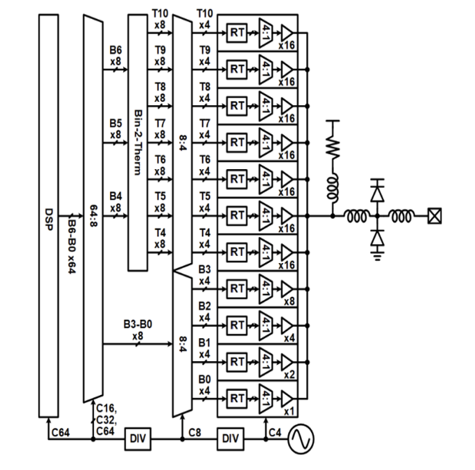 Figure 7. A 7b DAC-based quarter-rate TX example with seven thermometer and four binary output segments. Reproduced from A. Carusone et al., ‘Modern Wireline Transceivers,’ IEEE Journal of Solid-State Circuits, vol. 61, no. 2, pp. 395–422, Feb. 2026, licensed under CC BY-NC-ND 4.0.
This current cell is then scaled to a segmented architecture, which uses both unary and binary DACs. Unary (or thermometer code) uses unit-sized current sources arrayed in a 2x2 grid in layout to achieve better matching of current sources.
In many wireline transmitters, DAC resolution is kept modest, often around 6–7 bits, because channel loss, jitter, and front-end noise dominate before very fine quantization does.
Impairments
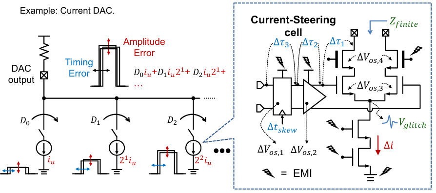 Figure 8. Impairments of Current steering DAC. Source: S. Su, “Principles and Practices of High-Speed Digital-to-Analog Converter Design” presented at the IEEE International Solid-State Circuits Conf. (ISSCC), San Francisco, CA, Feb. 15-19, 2026.
There are several impairments that cause both timing and amplitude errors:
- Time delay
- Voltage glitches
- Clock Skew
- Finite Input impedance
- EMI at all sources
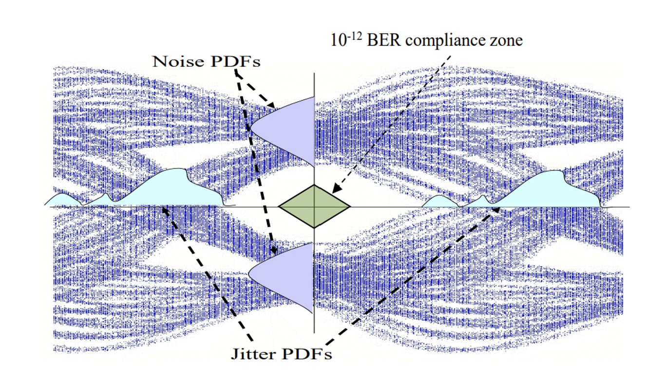 Figure 9. Jitter and Noise PDFs and how the affect BER. Source: M. Li. “Design and Verification for High-Speed I/Os at 10 to 112 to 224 Gbps, and 448 Gbps with Jitter, Signal Integrity, and Power Optimized: A Tutorial for Designcon 2026” DesignCon 2026
These impairments introduce timing and amplitude error at the system level. They translates to jitter in the x domain and noise in the y dimension. These effects directly affect the size of the “eye” at the RX side, so it is important to account for these and spec these appropriately.
RX Side - Time-Interleaved ADC
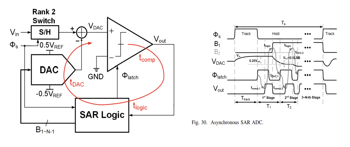 Figure 10. An Asynchronous SAR ADC with Timing Diagram. Reproduced from A. Carusone et al., ‘Modern Wireline Transceivers,’ IEEE Journal of Solid-State Circuits, vol. 61, no. 2, pp. 395–422, Feb. 2026, licensed under CC BY-NC-ND 4.0.
A common modern RX approach uses time-interleaved asynchronous SAR ADCs operating in a self-clocked manner.
In normal asynchronous SARs, it takes N clock cycles to complete an N bit conversion. In asynchronous circuits, self-clocking allows the completion of one comparison to automatically trigger the next.
Self-clocking removes the need for a very high external clock, but it makes the conversion timing dependent on timing delays and handshake robustness.
Asynchronous SARs are commonly used due to low comparator count, simple digital logic, and capacitive DACs for energy efficient operation at typical 6-7 bit resolution.
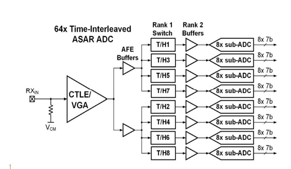 Figure 11. A Time-Interleaved SAR ADC. Reproduced from A. Carusone et al., ‘Modern Wireline Transceivers,’ IEEE Journal of Solid-State Circuits, vol. 61, no. 2, pp. 395–422, Feb. 2026, licensed under CC BY-NC-ND 4.0.
These SAR ADCs are time interleaved. The high speed data is “fanned out” to each of the sub-ADCs in order for their analog values to be digitalized. This is accomplished through a two-rank NxM interleaving scheme. This architecture performs sampling in two ranks:
- Rank 1 - Track and hold. The first rank tracks and holds the signal. The performance of these switches are critical as they sample the full BW signal.
- Rank 2 - Sample and hold buffer. These buffer the T/H signals to drive the parallel ADCs.
In modern PAM-4 112Gbps, the interleave factors range from 36-128 sub-ADCs depending on the layout area, with 64 being common. [1]
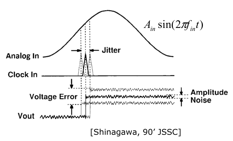 Figure 12. How Sampling / Clocking Jitter affects voltage error. Source: W. Chen, “Clocking and CDR Techniques for High Performance Wireline Transceiver” presented at the IEEE International Solid-State Circuits Conf. (ISSCC), San Francisco, CA, Feb. 15-19, 2026.
Impairments: There are several impairments:
- Skew and Jitter of clock
- Mismatches between sub-ADCs
These impairments translate timing mismatches into sampled voltage errors, often in a signal-dependent way, and can create both noise-like degradation and spurious tones.
Clocking Architecture
Perhaps the most important part of a high speed chip is the one everyone takes for granted: The clock.
The clock distribution becomes an increasingly important constraint as dimensions and speeds have scaled down. There are several challenges the clock faces:
- The clock needs to be recovered from the asynchronous RX data to ensure that the clock is in “sync” with the data to clock it appropriately
- The VCO needs to generate a reference clock with low jitter
- The time-interleaved blocks need some form of multi-phase clock to synchronize operations across parallel processing elements cleanly
- The parallel clock distribution needs minimal skew to minimize mismatches
After the pay wall I’ll describe the clocking architecture in more detail.
Inside the Silicon Machine is a reader-supported publication. To receive new posts and support my work, consider becoming a free or paid subscriber.
第二部分:解析(深度解读)
核心论点摘要
数据速率从 112Gbps 向 224Gbps、448Gbps 演进时,链路瓶颈已经从「数字逻辑能不能跑更快」转移到「模拟前端与片上物理约束能不能扛住」。信道损耗、噪声/抖动、片上寄生电容、模拟高阻极点共同限制了单线速率。现代 SerDes 的应对之道是两条范式转移:
- 处理向数字(DSP)迁移——用中等时钟频率(数 GHz 到十几 GHz)做大规模并行数字处理,把均衡、FEC 放到数字域;
- 高速模拟前端继续靠物理技巧突破——电流舵(current steering)最小化寄生电容充放电时间,时间交织(time interleaving)把单器件速度需求摊薄到大量并行 S/H、T/H 支路上。
原文把一条完整的 DSP-based 收发器数据通路拆开,逐块讲原理、损伤(impairments)与系统级影响。免费部分覆盖到 RX 时间交织 ADC;时钟架构(PLL/VCO/相位插值器/时钟分配)是付费深解,本文未含。
关键概念解读
- 电流舵电路(Current Steering):用恒定电流经差分开关导向电阻负载,核心优势是避免对寄生电容反复充放电,从而缩短建立时间;代价是静态功耗高(即使该 bit 关闭也耗电)。这是高速 MUX 单元和 DAC 单元的底层范式。
- 时间交织(Time Interleaving):与其把单个 ADC/DAC 做得更快,不如用 N 路并行、用「秩(rank)」化的 S/H、T/H 开关分摊速率。代价是时钟协调复杂度陡增(skew、jitter、支路失配都会转化成采样电压误差甚至杂散音调)。
- 分段电流舵 DAC(Segmented Current-Steering DAC):温度计码(unary/thermometer)用单位电流源阵列改善匹配,二进制码做高位;分辨率通常只做 6–7 bit——因为信道损耗、抖动、前端噪声在更精细量化之前就已经主导了系统误差,更细的 bit 没有性价比。
- 异步 SAR ADC(Asynchronous SAR):自时钟(self-clocking)让一次比较完成自动触发下一次,省掉极高外部时钟;依靠低比较器数、简单数字逻辑、电容 DAC 实现高能效,典型 6–7 位分辨率,再用 TI-ADC 把多路子 ADC 交织起来。现代 PAM-4 112Gbps 的交织因子常见 64(范围 36–128)。
分层拆解表:一条 DSP SerDes 数据通路
| 域 | 主要模块 | 作用 |
|---|---|---|
| TX | FEC → FFE(FIR 预失真)→ Serializer(半/ quarter-rate 时间交织)→ 高速 DAC → Driver | 编码、预均衡、串行化、数模转换、驱动 |
| Channel | Matching network → 传输线/铜缆 | 阻抗匹配防反射、衰减与失真 |
| RX | 前端(VGA + CTLE)→ TI-ADC → Deserializer → DSP | 放大均衡、模数转换、解串、数字域恢复 |
| Clock(付费) | CDR(Bang-Bang PD)→ LC-VCO PLL → 相位插值器 PI → 时钟分配(repeater/传输线/谐振器) | 从数据恢复时钟、低抖动参考、多相时钟、低 skew 分配 |
注意:边缘密度(edge density)是封装/板级硬约束——芯片边缘和铜缆能塞下的并行通道电路有限,所以「高速串行、单线高密度」成为必然,这恰恰是铜链路速率天花板的物理根源。
技术趋势
- 224G 已是现实,448G 在研:ISSCC 2026 已有大量 224G PAM-4 收发器与时钟/CDR 论文,448G 处于早期研发。
- DSP 与模拟协同设计成主流:数字域承担均衡/FEC,但模拟前端的非理想性(kickback noise、glitch、skew、失配)直接决定 RX 端「眼图」大小,是良率与性能的关键。
- 时钟架构是下一战场:多相时钟的相位插值器、低 jitter VCO、低 skew 分配在 448G 时代成为瓶颈——这也是作者把时钟单独列为付费深解的原因。
与本站其他文章的连接
本站已有大量 CPO(共封装光学)/ 高速光通信 系列文章。本篇 SerDes 拆解正好补上「铜链路侧」的技术底座:当单线铜互连撞上边缘密度与功耗墙,CPO 用光替代铜来继续 scaling 带宽——SerDes 的物理极限,正是 CPO 叙事的需求源头。可将本篇视为 CPO 系列在「电侧」的前置技术背景。相关阅读:本站 CPO 专题——CPO Fully Dissected、There Is No Such Thing As A CPO Stock、CPO Biggest Bottleneck: High Volume Testing 等。
风险提示
- 本文为技术科普解读,不构成投资建议;文中涉及的具体公司/论文仅作技术引用。
- 原文含付费墙,时钟架构细节未含,付费深解请以原作者付费内容为准。
- 原文为个人技术博客,图表多引自 ISSCC 2026 教程与 IEEE 论文,版权归原作者/出版方(多为 CC 署名许可),引用已标注来源。