Signal Integrity: A Primer — 信号完整性入门:通道损耗、抖动与 SerDes 架构的第一性原理
整理自 Chad Wallace(Silicon Co-Design, Substack)的技术科普:从 SerDes 的角色、铜互连的介质损耗与趋肤效应、随机/确定性抖动分类,到 BER 推算与 PAM-4/DSP 收发器架构趋势。英文原文 + 中文深度解读。
本文整理自 Chad Wallace (Substack / siliconcodesign.com) 的技术科普文章,原文发布于 2026-03-18。 标题原文:High-Speed Signal Integrity: Physical Impairments and Equalization Architectures。 结构为 正文(英文原文)+ 解析(中文深度解读),方便中英对照阅读。 ⚠️ 文末错误减少技术(FEC / 均衡 / CTLE / DFE / 如何达到更高数据速率)的详细展开在付费段,公开免费部分仅列出名称,本文如实标注、未含付费深解。
第一部分:正文(Original Article)
High-Speed Signal Integrity: Physical Impairments and Equalization Architectures
来源:Chad Wallace (Substack) · 2026-03-18
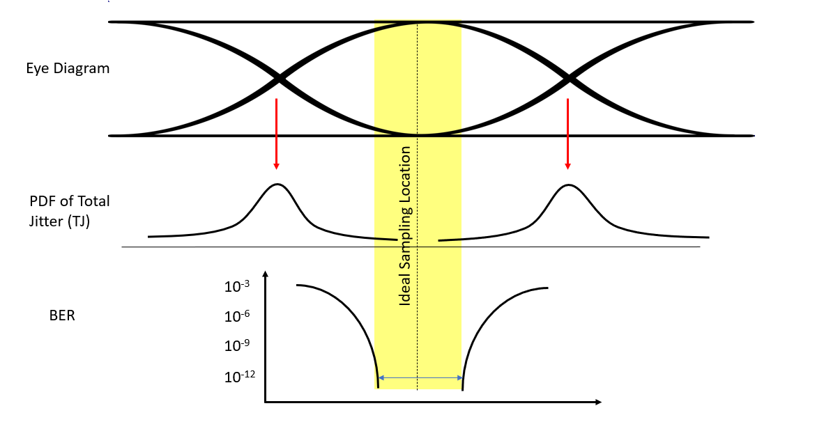
Figure 1. A Simplistic Overview for how Channel Loss and Jitter affect BER
In this post I cover the following topics:
SerDes - The Workhorse of chip to chip communication
The Root Causes of Signal-Integrity Degradation at High Speed
How Channel loss and Jitter degrade Bit Error Rate
Major System Trends:
PAM-4
DSP-based Architectures
🔒Error Reduction Techniques
🔒Forward Error Correction
🔒Equalization
🔒TX - Pre-emphasis / FFE
🔒RX - CTLE and DFE
🔒How to Achieve Higher Data Rate
Everyone talks about the importance of chip-to-chip communication, but few people appreciate the complexity hiding underneath it.
Signal integrity and SerDes architecture are often discussed as if they belong to different worlds: one in the lab and on the board, the other inside the chip. In reality, they are deeply coupled.
My goal in this post is to show how signal-integrity constraints at the channel and board level—loss, jitter—affect performance through BER and ultimately drive complexity back into the transceiver itself, shaping choices in equalization, clocking, and data conversion. Here I’ll focus on the signal-integrity foundations from first principles, then build on that in a follow-up post on chip architecture.
Much of the content of this post is material consolidated from a Tutorial given by Dr. Mike Peng Li from DesignCon 2026, the premier high-speed communications conference, as well as from ISSCC, academic papers and SI books. Figures are reproduced for commentary and educational purposes.
SerDes - The Workhorse of chip to chip communication
A serializer-deserializer (SerDes) converts parallel digital data into a high-speed serial stream for transmission, then reconstructs it at the receiver. This allows systems to move large amounts of data between chips and systems without requiring a huge number of parallel wires.
SerDes and optical links are the “workhorses” of communication within data centers in “scale up” and “scale out” networks:
Chip to chip
Modular top chip copper links on a PCN and an optical module
Between a CPU and network interface
Backplane and midplane links over backplane PCBs or passive copper cables
SerDes is what enables parallel computing across many CPUs and GPUs as a means of data distribution.
Historically, many SerDes architectures have been analog-based. SerDes speeds have scaled with PAM-2 (NRZ) signals over time to meet the growing needs of traditional computing.
Then, AI and chiplets came in and started demanding more data.
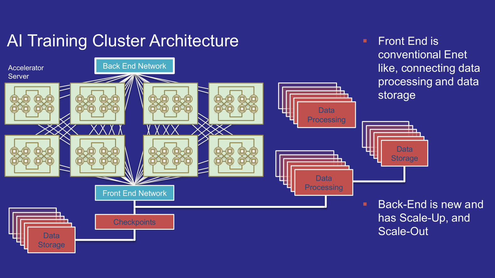
Figure 2. A System level AI Training Cluster rack diagram of scale-up and scale-out networks where SerDes and optical dominate chip to chip communication. Source: M. Li. “Design and Verification for High-Speed I/Os at 10 to 112 to 224 Gbps, and 448 Gbps with Jitter, Signal Integrity, and Power Optimized: A Tutorial for Designcon 2026” DesignCon 2026
These two technological trends put a lot of pressure on chip-to-chip communication to get faster and reach farther due to the massive amounts of data movement:
AI workloads involve massive data movement: repeated memory access, movement of intermediate results, and parallel processing across many GPUs in a rack.
Chiplets disaggregate a system into multiple smaller dies, which must then be tied back together through high-speed chip-to-chip interfaces.
However, as data demands push speeds higher and links longer, fundamental physics begins constraining performance:
Channel loss due to higher attenuation at higher frequencies
Jitter budgets getting tighter
Transmission line effects that cause distortions
Noise that can cause errors
These add complexity to the SerDes to correct for. Unfortunately, the added complexity makes it more challenging to understand how one part of the system affects the other, such as:
How jitter in the VCO eats into the timing margin needed to meet the target BER
How receiver clock skew and TI-ADC area constraints affect sampling margin, data throughput, and calibration burden
In the following sections I’ll be focusing on signal integrity fundamentals from first principles. The goal is to ask:
What are the fundamental physics constraints limiting performance?
What complexity in the chip architecture is needed to scale speeds beyond 112.5Gbps to 224Gbps and eventually 448Gbps?
The Root Causes of Signal-Integrity Degradation at High Speed
In this section, I’ll focus on describing two primary causes of signal-integrity degradation at high speeds: channel loss, and jitter. I’ll then show how they affect BER.
Channel loss in Copper interconnects
Copper is widely used as the interconnect of choice to transmit signals between chips due to its high electrical conductivity and durability.
Copper has been used for many years at low data rates where the losses were much less. However, the loss increases at higher signal frequencies. There are two major loss mechanisms:
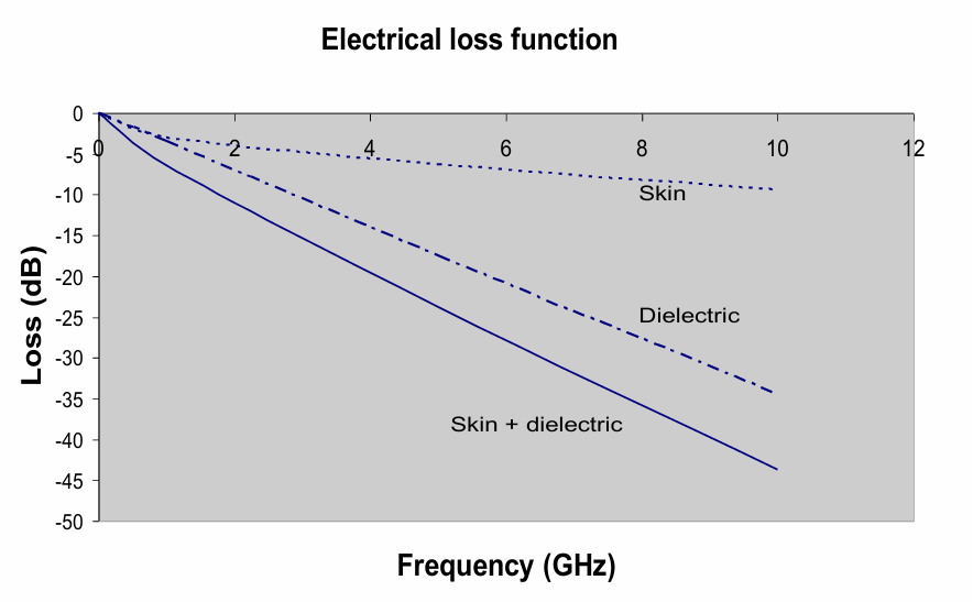
Figure 3. Copper Loss (skin and dielectric) as a function of frequency. Source: M. Li. “Design and Verification for High-Speed I/Os at 10 to 112 to 224 Gbps, and 448 Gbps with Jitter, Signal Integrity, and Power Optimized: A Tutorial for Designcon 2026” DesignCon 2026
Dielectric loss. Dielectric loss occurs due to heat energy dissipation of dipoles at high frequencies. A quickly alternating electric field in the dielectric causes polarization in dipoles in the dielectric (i.e. the positive and negative parts of the atom move apart) and results in energy dissipation through heat.
Dielectric loss scales with frequency and is generally the dominant loss mechanism at the data rates that modern SerDes nowadays run at.
Skin effect. Skin effect occurs when time-varying electromagnetic fields push current toward the edges of the conductor. This results in an effective lowering of the cross-sectional area that the signal actually “sees”.
Skin-effect loss scales roughly with the square root of frequency and has historically been a major source of channel loss until dielectric loss becomes more dominant at higher frequencies.
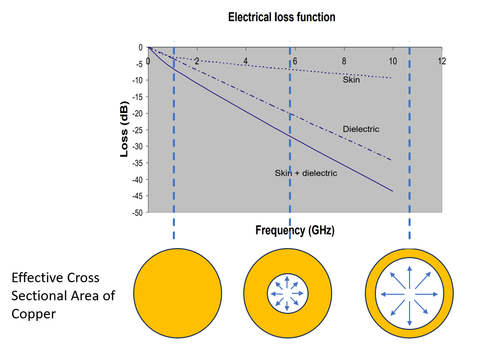
Figure 4. Skin effect in copper: As frequency increases, the current flows along the edge of the copper, lowering the effective sectional area it sees and increases attenuation. Source: M. Li. “Design and Verification for High-Speed I/Os at 10 to 112 to 224 Gbps, and 448 Gbps with Jitter, Signal Integrity, and Power Optimized: A Tutorial for Designcon 2026” DesignCon 2026
In both cases, signal attenuation increases with frequency. This means that signals with multiple frequency components like square waves will have higher order frequencies attenuated more strongly. This will result in a “rounding” of the signal at the other end with degraded amplitude.
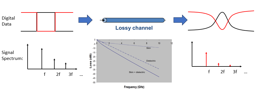
Figure 5. The effect of a lossy channel on an ideal square wave pulse. Higher order frequency components get attenuated more strongly and the signal appear to be rounded at the other end.
Modern 112G PAM4 systems typically target 25 dB to 35 dB of channel loss.
Jitter
Jitter is defined as the time variation in when a signal edge actually transitions compared to its ideal transition point. Jitter is a significant limiter of performance in high-speed applications because it affects how much of a time “window” you have to accurately sample the digital data.
Jitter is broadly broken down into two major categories: Random and Deterministic:
Random Jitter comes from noise-like mechanisms that are fundamentally statistical in nature, such as thermal noise.
This is always uncorrelated and typically modelled as a Gaussian distribution due to the central limit theorem that states that summing up a variety of PDFs from uncorrelated sources tend toward a Gaussian distribution.
Deterministic Jitter is jitter from repeatable structure in the system such as data movement and reflections.
This jitter is typically bounded with a max and min timing shift - the edge shifts in a repeatable way. It can also be correlated or uncorrelated. Examples include:
Data dependent jitter (ISI) - Symbols from previous transitions spill into the next time window
Periodic Jitter
Bounded uncorrelated jitter
As link complexity has grown, many other jitter sources must be accounted for during design and measured in silicon.
How Channel loss and Jitter degrade Bit Error Rate
Both losses distort the signal in complementary ways:
Channel loss distorts the waveform itself by attenuating and smearing its higher-frequency content
Jitter introduces uncertainty in when transitions occur.
Together, these (and other effects such as reflections) reduce eye opening and increase the Bit error rate (BER) at your sampling edge.
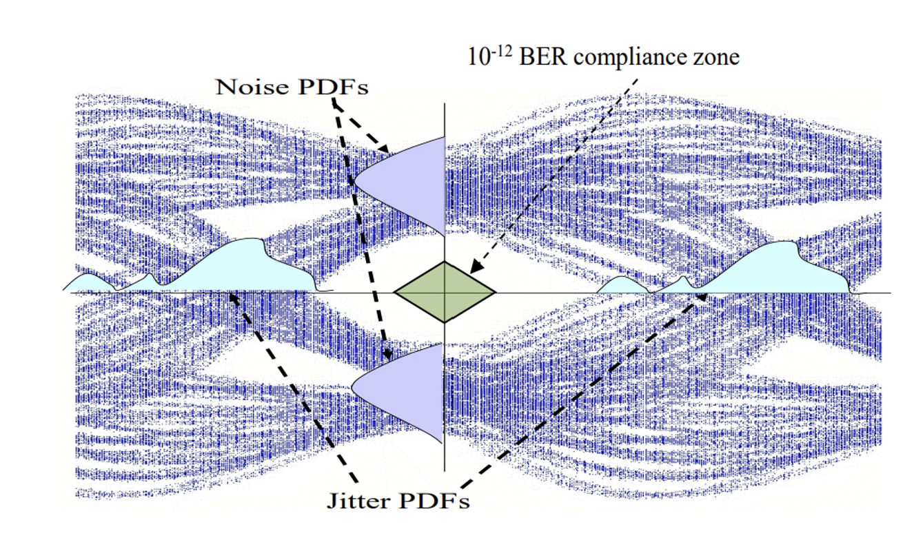
Figure 6. A typical eye diagram showing both the effect of channel loss (rounding) and jitter (signal amplitude and timing uncertainty). Source: M. Li. “Design and Verification for High-Speed I/Os at 10 to 112 to 224 Gbps, and 448 Gbps with Jitter, Signal Integrity, and Power Optimized: A Tutorial for Designcon 2026” DesignCon 2026
Bit error rate is not easy to measure directly because of the amount of time it takes to observe enough samples (sometimes trillions) to get a statically significant measurement of BER. It is usually easy to measure a BER of 10^-6 which is 1 error in 1 million bits with a BERT (Bit error rate tester), but some systems require BERs of 10^-12 which is one error in one-trillion bits!
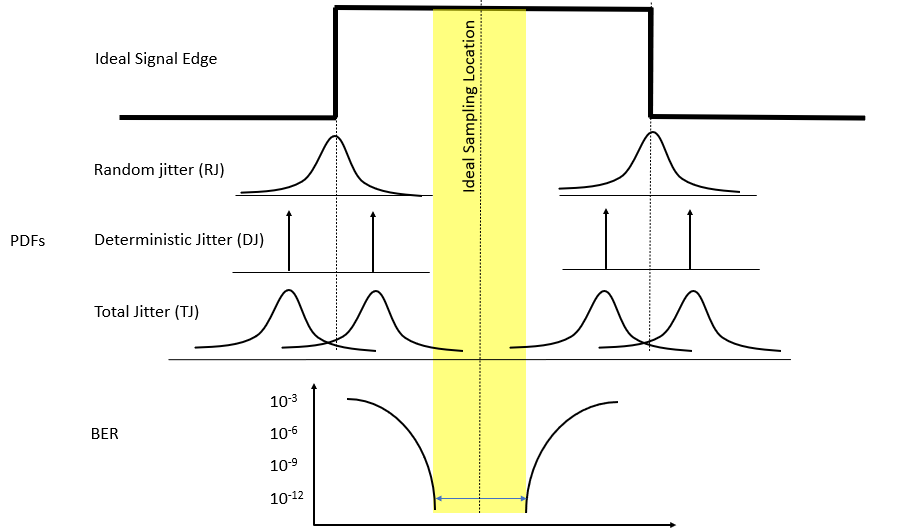
Figure 7. How Jitter components and BER are related
Often, lower BERs are often extrapolated from higher BER curves. The Dual-Dirac model is a widely accepted “worst case model” used to extrapolate this. To show how BER is driven from jitter, consider the two major classes of jitter:
RJ spreads the signal edge according to a Gaussian distribution
DJ shifts the signal edge with two “bounds”. In this model, the worst cases are represented as two worst case impulse “spikes” at either bound.
(Note that this is not the actual PDF of the DJ as it varies in uniformity within the bounds. However, this works fine because we only care about the “tails” of the RJ curve convolved at the bounds)
These two sources combine in a “convolution” format, so the gaussians of the RJ map onto the bounds of the DJ to obtain the Total Jitter (TJ). The BER is then estimated from the tails of the total-jitter distribution: as the distribution spreads further into the sampling margin, the probability of error increases.
You can then use this to map contours of constant BER in the center of the eye that decrease the more the signal is sampled at the center of the eye:
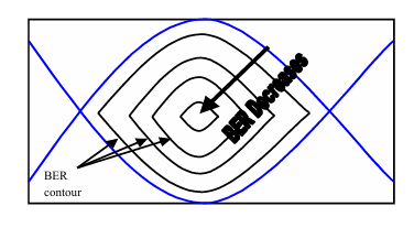
Figure 8. Contours of constant BER. Source: M. Li. “Design and Verification for High-Speed I/Os at 10 to 112 to 224 Gbps, and 448 Gbps with Jitter, Signal Integrity, and Power Optimized: A Tutorial for Designcon 2026” DesignCon 2026
Major System Trends: PAM-4 and DSP-based Architectures
PAM-4: 4 level pulse amplitude modulation
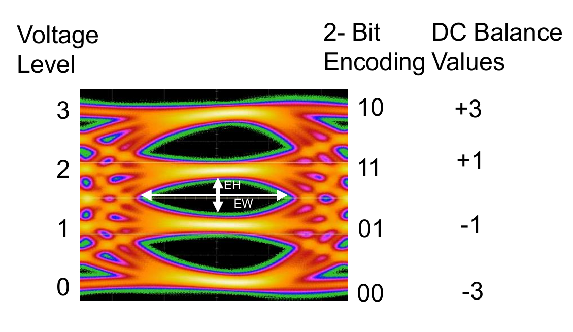
Figure 9. PAM-4 Modulation. Source: M. Li. “Design and Verification for High-Speed I/Os at 10 to 112 to 224 Gbps, and 448 Gbps with Jitter, Signal Integrity, and Power Optimized: A Tutorial for Designcon 2026” DesignCon 2026
PAM-4 uses four levels of modulation instead of two. This allows you to transmit two bits per symbol while halving the required symbol rate for a given bit rate.
However, added signal levels make PAM-4 more sensitive to noise, nonlinearity, ISI, and timing jitter. It also requires DACs to generate the four analog levels. There are also more transition combinations to account for.
DSP-Based Transceivers
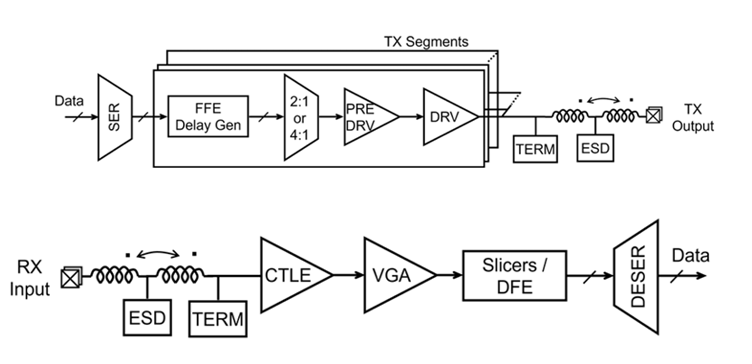
Figure 10. Analog-based Transceiver architecture for short reach. Reproduced from A. Carusone et al., ‘Modern Wireline Transceivers,’ IEEE Journal of Solid-State Circuits, vol. 61, no. 2, pp. 395–422, Feb. 2026, licensed under CC BY-NC-ND 4.0.
When data speeds were slower, most of the processing came from analog circuits that were sufficient to perform the signal conditioning needed to achieve good BERs. Figure 9 shows a typical short-reach, analog-based transceiver with common building blocks.
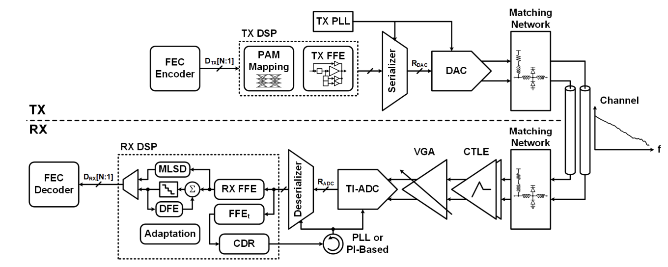
Figure 11. DSP-Based Transceiver architecture. Reproduced from A. Carusone et al., ‘Modern Wireline Transceivers,’ IEEE Journal of Solid-State Circuits, vol. 61, no. 2, pp. 395–422, Feb. 2026, licensed under CC BY-NC-ND 4.0.
As speed and throughput increased, most architectures added a lot of DSP along with the analog blocks. Digital allows a lot more programmability to handle data processing with FIR/IIR filters. However, digital also adds a large amount of peripheral complexity to handle the speed it needs, including:
The ADC/DACs needed to convert between the analog and digital domains
The clocking architecture to clock the circuits
Error Reduction Techniques
After the paywall, I’ll cover key error reduction techniques, including equalization, FEC, CTLE, and DFE.
第二部分:解析(深度解读)
一、核心论点摘要
本文从第一性原理出发,系统讲解了高速芯片间通信中信号完整性(Signal Integrity)的物理基础,核心逻辑线:
- SerDes 是 AI 数据中心 chip-to-chip 通信的主力——所有 GPU 互联、chiplet 内 die-to-die、背板/中板连接都依赖它。
- 两大物理退化机制:铜互连的通道损耗(介质损耗 + 趋肤效应)随频率升高急剧恶化;抖动(随机抖动 RJ + 确定性抖动 DJ)压缩采样时间窗口。
- 两者耦合 → 眼图缩小 → BER 上升 → 需要通过 PAM-4、DSP 架构等手段补偿。
- 架构趋势:从纯模拟收发器到 DSP-based 收发器,数字域带来了可编程性但引入了 ADC/DAC 和复杂时钟架构的额外负担。
⚠️ 付费段内容(FEC、CTLE、DFE、TX 预加重等均衡技术的详细展开)未含。
二、关键概念解读
2.1 通道损耗的两种物理机制
| 机制 | 物理本质 | 频率依赖性 | 现代 SerDes 中地位 |
|---|---|---|---|
| 介质损耗(Dielectric Loss) | 高频交变电场使介质中偶极子极化→热能散逸 | ∝ f | 112G PAM4 速率下主导 |
| 趋肤效应(Skin Effect) | 时变电磁场将电流推向导体表面→有效截面积减小 | ∝ √f | 历史上主导,高频下退居次要 |
投资视角:介质损耗是材料物理瓶颈,意味着即使工艺进步、信号调理再强,PCB 板材(低损耗介质如 Megtron 等)和封装基板本身就构成硬天花板。这也是为什么 CPO(共封装光学)被寄予厚望——光在光纤中的损耗远低于铜介质损耗。
2.2 抖动分类框架
1
2
3
4
5
6
7
抖动(Jitter)
├── 随机抖动(Random Jitter, RJ)
│   └── 热噪声等,无界、高斯分布、不可预测
└── 确定性抖动(Deterministic Jitter, DJ)
    ├── 数据相关抖动(ISI)——前一符号拖尾进入当前窗口
    ├── 周期性抖动(Periodic Jitter)
    └── 有界非相关抖动(Bounded Uncorrelated Jitter)
RJ + DJ 通过卷积组合成总抖动(Total Jitter, TJ),BER 由 TJ 分布的尾部决定。Dual-Dirac 模型是目前工业界广泛接受的”最坏情况”外推方法——用两个 Dirac 脉冲代表 DJ 的边界,再将 RJ 的高斯分布叠加在边界上。
投资视角:任何做高速 SerDes IP(如 Synopsys、Cadence、Alphawave、Rambus)或高速测试设备(如 Keysight、Tektronix)的公司,其产品价值直接与”能在多少 dB 损耗和多少 ps 抖动下保证目标 BER”挂钩。这是评估技术壁垒的核心指标。
2.3 PAM-4 vs NRZ(PAM-2)
| 参数 | NRZ (PAM-2) | PAM-4 |
|---|---|---|
| 每符号比特数 | 1 | 2 |
| 给定比特率下符号率 | R | R/2 |
| SNR 要求 | 低 | 高约 9.5 dB |
| 对噪声/非线性敏感度 | 低 | 高 |
| 是否需要 DAC | 否 | 是 |
PAM-4 的本质权衡:用 SNR 换带宽效率。符号率减半意味着通道损耗更低(因为高频分量减少),但四电平使眼图垂直开口缩小到 1/3,对任何幅度噪声都更敏感。
2.4 模拟 vs DSP 收发器架构
| 维度 | 模拟收发器 | DSP-based 收发器 |
|---|---|---|
| 信号处理 | 模拟滤波器/均衡器 | FIR/IIR 数字滤波 |
| 灵活性 | 低 | 高(可编程) |
| 功耗 | 低 | 高(ADC/DAC + 数字逻辑) |
| 面积 | 小 | 大 |
| 适用速率 | 低速/中速 | 112G+ PAM4 |
DSP 架构的核心代价是外围复杂度:ADC/DAC 本身需要高线性度、高带宽,时钟架构(PLL)也要满足极低抖动要求。这形成了一个复杂度正反馈循环——越高速越需要 DSP,DSP 越复杂对时钟和 ADC 要求越高。
三、与本站其他文章的连接
- 光通信系列:本文的 SerDes 和通道损耗是理解”为什么需要光互联”的前提——铜上的损耗和抖动正是推动 CPO/硅光的关键驱动力。参见光通信入门。
- PLL 入门:SerDes 中的时钟恢复和频率合成高度依赖 PLL。参见PLL 入门。
- 光投资地图:信号完整性瓶颈 → 光互联需求 → CPO/硅光投资机会,参见光投资地图 v1.0。
四、风险提示
- 铜互联短期不可替代:尽管光互联是趋势,在 chiplet 片间互联(UCIe)、板级互联中铜仍然是成本最优方案,SerDes IP 市场仍在高速增长。
- DSP 架构的功耗瓶颈:112G→224G→448G 的演进中,DSP-based 收发器的功耗增长可能不可持续,模拟辅助/全模拟均衡方案(如基于 CTLE+DFE 的无 DSP 方案)可能在某些场景回归。
- 技术路线不确定性:224Gbps 的行业标准(OIF/CEI-224G)仍在演进中,不同厂商的 SerDes 架构差异大,需关注标准统一进程。