The Phase-Locked Loop: A Primer — 锁相环入门:从系统架构到 Type I/II PLL 的直观理解
整理自 Chad Wallace(Silicon Co-Design, Substack)的技术科普:从 PLL 的「管弦乐队指挥」比喻出发,深入 Type I(XOR+RC LPF)与 Type II(电荷泵)PLL 的架构差异、Bode 图对比、以及二阶传递函数的推导。英文原文 + 中文深度解读。
本文整理自 Chad Wallace (Substack / siliconcodesign.com) 的技术科普文章,原文发布于 2026-02-11。 结构为 正文(英文原文)+ 解析(中文深度解读),方便中英对照阅读。 ⚠️ 文末晶体管级实现(PFD / 电荷泵 / VCO / LC 振荡器 / 环形振荡器)、相位噪声与抖动分析、以及分数分频合成器的详细展开在付费段,公开免费部分仅列出名称,本文如实标注、未含付费深解。
第一部分:正文(Original Article)
The Phase Locked Loop: A Primer
来源:Chad Wallace (Substack) · 2026-02-11
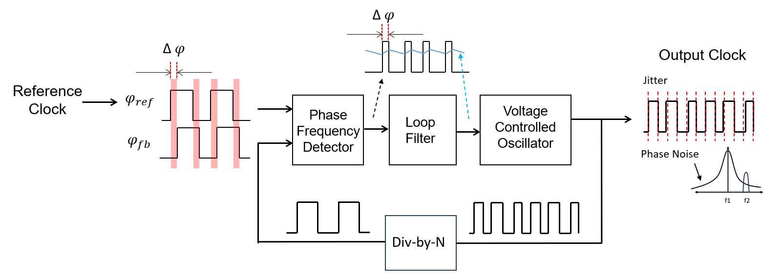
Figure 1. A look into the features of a Phase Locked Loop
This post covers the following topics:
High level design principles
An Intuitive Look into Type I and Type II Phase Locked loops
Type 1 PLL: XOR and RC LPF
Type 2 PLL: Charge Pump
Bode Plots Comparison for Type I and II PLLs
The Transfer Function of the type II PLL
🔒Common transistor level implementations of type II PLLs
🔒Phase-Frequency detector
🔒Charge Pump
🔒Voltage Controlled Oscillator
🔒LC Oscillator
🔒Current Starved Ring oscillator
🔒Important considerations: Phase Noise and Jitter
🔒A high-level look into the Fractional-N Synthesizer
A modern chip is like a finely tuned orchestra. Each member of the orchestra knows their role and what notes to play, but needs to know when to play them. The conductors role is to align musicians to a shared interpretation of tempo.
Imagine if there was no conductor; musicians don’t know when to play, so the orchestra gets out of sync really quickly as each person plays to their own tempo.
This is the role PLLs play in circuits: as the “conductor” that produces a clock to keep blocks synchronized to a common reference. PLLs help shape and distribute timing under real noise and delays.
The PLL is a beautifully complex and common circuit in ICs that reward high-level analog-design intuition. That is, begin at the architecture level, make sure your design is feasible, and work your way down to transistor level implementation.
At its core, phase locked loops generate clocks from a reference source. This sounds simple, but actually finds use in a wide variety of applications:
Frequency Synthesis: Generate a range of frequency multiples for sampling, DSP, SerDes, RF LO, etc…
Clock Recovery: Recover data from a bit stream of asynchronous data without a clock reference
RF Channel Selection: Select channels across specific frequency channels in transceivers
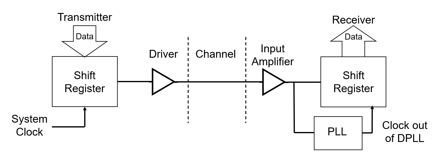
Figure 2. Example application of a PLL in a digital communication system. Adapted from “R. Jacob Baker. ‘CMOS Circuit Design, Layout, and Simulation, Revised Second Edition.’” p. 551 [1]
The question is, why do you need a PLL anyways? Why can’t you just use a reference clock?
Well there are a number of reasons:
Generating internal clocks from a reference - different parts of a system need different internal clock frequencies at different multiples.
Frequency tuning - The PLL frequency can be tuned by controlling parameters
Shaping jitter / phase noise - A PLL “reshapes” noise from a reference source and can be optimized in a way to minimize it. Inside the loop bandwidth, the reference/PFD-path noise tends to dominate; outside that bandwidth, the VCO noise dominates.
Clock skew compensation - In systems with long signal distribution, A PLL can adjust for signal delays across the chip by adjusting its “phase” to be in sync with the original clock.
I want to give a survey level overview of the major design considerations of a PLL at different abstraction levels, from system level, to transistor level, to noise analysis. More detailed information can be found in the book “Design of CMOS Phase-Locked Loops” by B. Razavi [2].
High level design principles
The idea with system architecture is to detect problems at the highest possible level of abstraction.
Typically, at this stage, global stability is owned by the architecture. The architect models the transfer function of the PLL architecture through gain, integrator, and filter blocks.
At this stage there are several things modelled:
Speed - how high are the frequencies needed?
Loop bandwidth and phase margin - how fast does the loop need to be to meet the lock time / overshoot requirements?
Tuning Range - What range of frequencies need to be supported? What VCO gain is required to support this frequency range?
Capture range - What range can the PLL pull-in from unlocked?
Lock/hold range - What is the frequency range over which the PLL stays locked once locked?
Sensitivity - What are the worst case corners with respect to global / random variations? What are critical mismatch sensitivities?
Noise - Where are the major contributors of noise to the output jitter / phase noise?
Spurs - where are reference spurs and fractional spurs?
These issues are investigated in a high level modelling language like VerilogAMS or Simulink.
More local stability issues can be left to transistor level designers like op amp phase/gain margin and gain-bandwidth tradeoffs.
The worst thing you want is to jump to transistor level design with a process and find you can’t implement the frequency or obtain the desired phase noise with the given process!
An Intuitive Look into Type I and Type II Phase Locked loops
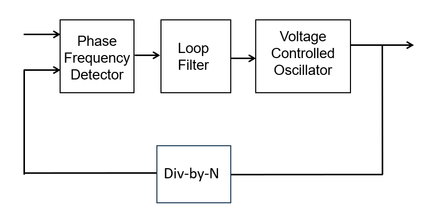
Figure 3. Major Blocks in the PLL
The basic idea behind a PLL is that it is a closed-loop system designed to synchronize the output clock to the input reference, whether that be a:
Crystal oscillator
External system clock
Data stream
It does this with the following blocks:
Phase-Frequency detector: Responds to both phase and frequency differences and generates a stream of pulses.
- Note that “Phase detector” is used in type I PLLs like in the XOR gate, where the frequencies are already close.
Loop Filter: Filters the input to provide a control voltage Vctrl into the voltage controlled oscillator
Voltage Controlled Oscillator: Produces an output frequency as a proportion of the input control voltage with a loop gain:
Divide-by-N Counter: Divides the output frequency down by integers of N, allowing the output frequency to be a multiple of the input frequency and the resulting divided clock to be compared against the reference.
The PLL “captures” the frequency from an initial value and adjusts itself until the reference frequency tracks the input frequency. Below is an example of a PLL locking to 7.5MHz in 80us from startup:
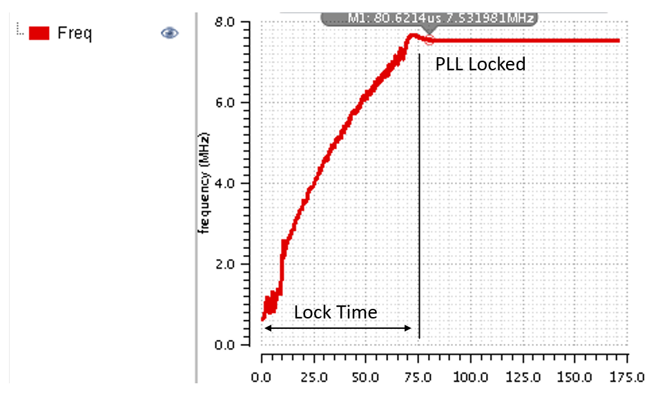
Figure 4. A PLL Locking to 7.5MHz in 80us
Ideally, when a PLL is in “lock”, the average frequency matches and the phase error settles to a small constant (nearly 0). The voltage on the VCO is a DC value with periodic “ripples” to micro adjust the frequency.
The dynamics of a PLL are similar to damped oscillator systems, with a few different “types” of PLLs:
Type 1 PLL: XOR and RC LPF
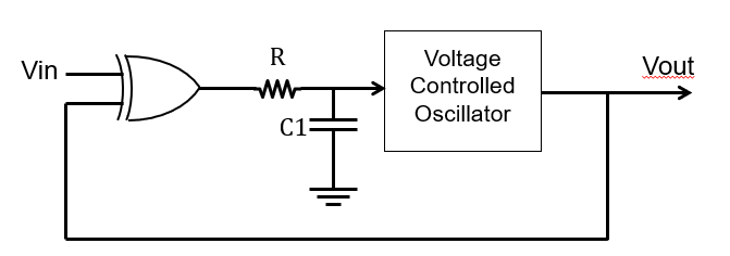
Figure 5. A Simple Type I PLL with an XOR and an RC LPF
In a simple implementation, one can simply implement the above with an XOR and and RC Low pass filter.
It is type I because it only has 1 integrator:
- The VCO
So it has one pole at the origin, and another pole at the RC corner frequency.
However, there are two drawbacks:
Poor lock acquisition - A type 1 PLL often needs the VCO to be initialized close to the target, or else acquisition can be slow or fail without an initialization mechanism
Non-zero static phase error in lock - In lock, a Type I loop typically requires a constant phase offset to sustain the DC control voltage.
Type 2 PLL: Charge Pump
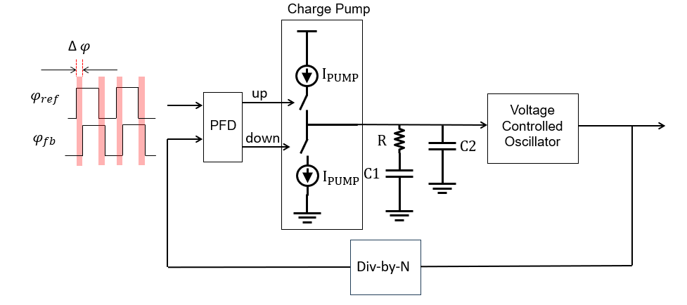
Figure 6. A Type II PLL using a charge pump controlled with “Up” and “down” signals and an RC Filter to stabilize the voltage fed to the VCO
The Charge Pump is a common block used that sources / sinks current into the filter.
Charge Pump PLLs are considered Type II because this system has 2 integrators:
The VCO
The Charge pump current pulses + loop filter capacitor that integrates current to voltage
There are two poles at the origin, and a zero formed by the R.
C2 is added as a high frequency bypass to reduce voltage ripples across Vctrl. C2 is usually smaller, about 1/10 or 2/10 of C1.
Type II integrators can drive steady state error to 0 even with a constant frequency offset, allowing for better tracking and acquisition.
Bode Plots Comparison for Type I and II PLLs
The open loops gains are different for type I and II. Notice how in the type II case, the R introduces a zero that adds phase lead (+90 deg), improving phase margin and stability.
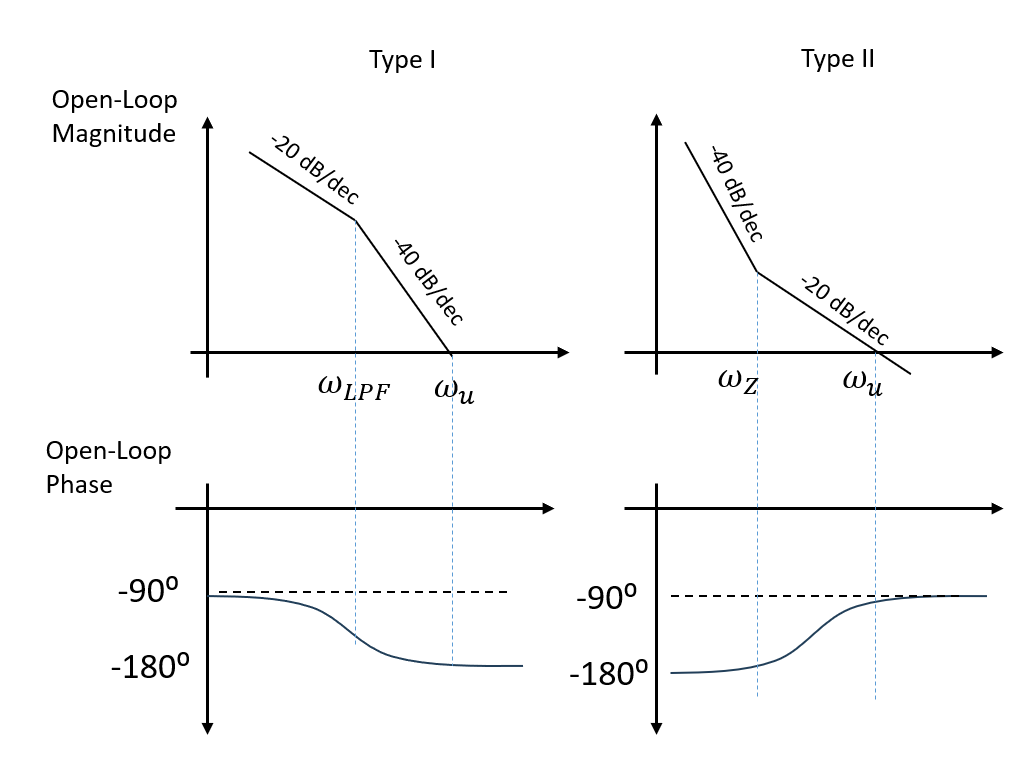
Figure 7. Bode Plot Comparison of Type I and II PLLs
The Transfer Function of the type II PLL
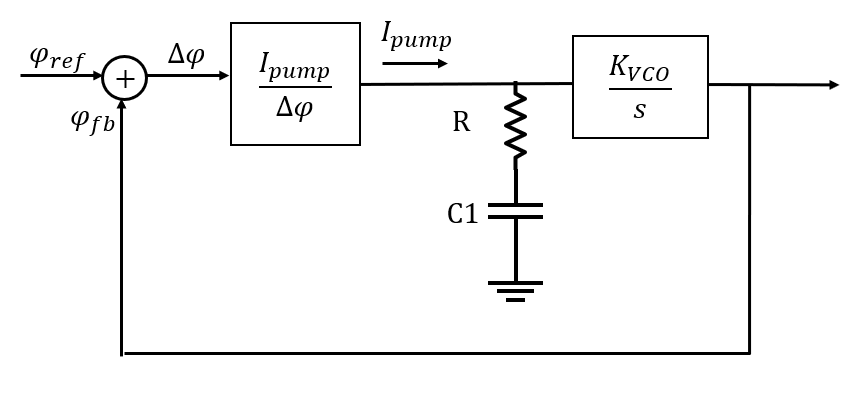
Figure 8. Transfer Function of each major block
To design a PLL, one must first understand its dynamics through a transfer function. Note that C2 is neglected from this analysis because its value is small compared to C1.
In this derivation, the loop variable is phase, and gains are expressed in the usual PLL units (PFD/CP gain and VCO gain).
The open loop transfer function is given by:
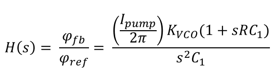
To obtain a closed loop transfer function from an open loop form H(s) and Feedback component G(s):
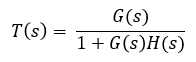
Substituting H(s) into the above:
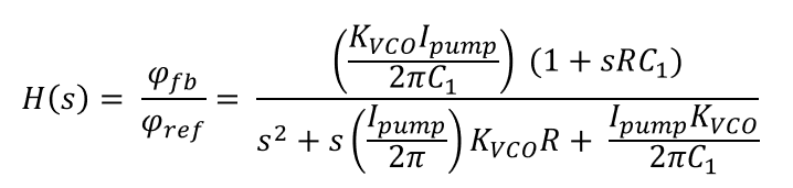
There’s a lot of terms here, but the key thing is that this is a second order transfer function of the form:
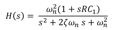
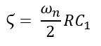
With damping factor:
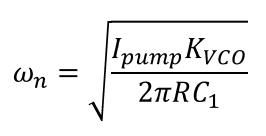
And natural frequency:
If you recall second order transfer functions, the output “response” can be over or underdamped.
Now that we’ve seen the blocks and built some intuition, we can add additional layers of understanding on top of it. After the paywall we’ll define the common blocks that are used, define where noise and jitter show up, and give a high-level introduction to fractional-N PLLs.
第二部分:解析(深度解读)
一、核心论点摘要
本文用一个优雅的比喻开场——芯片如管弦乐队,PLL 就是指挥——然后逐层深入 PLL 的系统架构设计哲学:
- 架构先行:先在最高抽象层(VerilogAMS/Simulink)验证全局稳定性、环路带宽、相位裕度、调谐范围、噪声预算等,再下到晶体管级——”在最坏的事就是在晶体管层才发现工艺达不到目标频率”。
- Type I vs Type II:核心区别在于积分器数量——Type I 只有一个(VCO),Type II 有两个(VCO + 电荷泵+环路电容),导致锁相精度和捕获性能的本质差异。
- 传递函数:Type II PLL 是二阶系统,阻尼因子 ζ 和自然频率 ωn 决定了锁相速度和过冲特性。
⚠️ 付费段内容(PFD/CP/VCO 晶体管级实现、相位噪声与抖动分析、分数-N 合成器)未含。
二、关键概念解读
2.1 PLL 四大功能模块
| 模块 | 功能 | 关键指标 |
|---|---|---|
| 鉴频鉴相器(PFD) | 比较参考时钟与反馈时钟的相位/频率差,输出 UP/DN 脉冲 | 死区(dead zone)、最大工作频率 |
| 环路滤波器(Loop Filter) | 平滑 PFD 输出脉冲,产生 VCO 控制电压 Vctrl | 带宽、相位裕度 |
| 压控振荡器(VCO) | 将 Vctrl 转换为频率输出 | 增益 Kvco、调谐范围、相位噪声 |
| N 分频器(Divider) | 将输出频率除以 N,使反馈频率等于参考频率 | 分频比范围、工作频率 |
2.2 Type I vs Type II PLL 对比
| 维度 | Type I(XOR + RC LPF) | Type II(电荷泵) |
|---|---|---|
| 积分器数量 | 1(仅 VCO) | 2(VCO + 电荷泵/电容) |
| 稳态相位误差 | 非零——需要恒定相位差维持 DC 控制电压 | 零——即使有频率偏移也能驱动到零 |
| 锁相捕获 | 差——需要 VCO 初始频率接近目标 | 好——频率捕获范围更宽 |
| 极点 | 原点 1 个 + RC 转角处 1 个 | 原点 2 个 + R 引入的零点 |
| 零/极点补偿 | 无 | R 产生零点,提供 +90° 相位超前 |
| 高频纹波抑制 | — | C2(约为 C1 的 1/10~2/10)作高频旁路 |
关键直觉:Type II 的电荷泵 + 环路电容将电流积分成电压,这相当于增加了一个积分器。数学上这意味着系统类型从 Type I 升到 Type II(增加了原点处的极点),从而可以跟踪频率阶跃(斜坡输入)而稳态误差为零。但代价是稳定性更难设计——引入的 R 产生零点就是为了补偿稳定性。
2.3 二阶传递函数的物理直觉
Type II PLL 的闭环特性是一个二阶低通系统:
- 阻尼因子 ζ:决定锁相过程的过冲/振铃程度。ζ < 1 → 欠阻尼(快速但有振铃),ζ > 1 → 过阻尼(无振铃但慢),ζ ≈ 0.707 → 最优(经典的 Butterworth 响应)。
- 自然频率 ωn:决定环路带宽。ωn 越大,锁相越快,但噪声抑制能力下降(环路带宽内参考噪声主导,带宽外 VCO 噪声主导)。
设计权衡:
- 大 ωn → 快锁相、好 VCO 噪声抑制 → 但更多参考/PD 噪声进入
- 小 ωn → 好参考噪声抑制 → 但慢锁相、VCO 噪声更突出
2.4 PLL 噪声整形特性
文中提到一句关键话:”Inside the loop bandwidth, the reference/PFD-path noise tends to dominate; outside that bandwidth, the VCO noise dominates.”
这背后的物理是:
- PLL 的闭环传递函数对参考路径噪声是低通特性 → 低频噪声(参考晶振、PFD)直通到输出
- 对VCO 噪声是高通特性 → 高频噪声(VCO 本身)直通,低频被环路抑制
所以环路带宽的选择本质上是两种噪声源的 trade-off。
2.5 PLL 的主要应用场景
| 应用 | 场景 | 关键技术要求 |
|---|---|---|
| 频率合成 | 为 ADC/DAC/DSP 产生采样时钟、RF 本振 | 宽调谐范围、频率精度 |
| 时钟恢复 | 从无时钟参考的异步数据流恢复时钟(SerDes CDR) | 低抖动、快速锁定 |
| RF 通道选择 | 收发器中按频率通道切换 | 频率分辨率、切换速度 |
三、分层设计方法论
文章反复强调的架构优先思想对投资者也很重要:
1
2
3
4
5
6
7
8
9
高层建模(VerilogAMS/Simulink)
├── 全局稳定性、环路带宽、相位裕度
├── 调谐范围、捕获/锁定范围
├── 灵敏度/失配分析
└── 噪声预算 / 杂散分析
        ↓
晶体管级设计
├── 运放相位/增益裕度
└── 增益带宽权衡
投资视角:这意味着评估一家做 PLL IP 的公司的技术壁垒,不仅要看其能跑多高频率,还要看:噪声性能(jitter spec)、功耗效率、工艺可移植性、以及是否具备全流程从系统建模到版图实现的能力。
四、与本站其他文章的连接
- 信号完整性:SerDes 中时钟恢复(CDR)的核心就是 PLL,抖动分析直接决定 BER。参见信号完整性入门。
- 光通信:光模块中的 SerDes 和 DSP 都需要 PLL 提供低抖动时钟,PLL 的相位噪声直接影响光通信的链路预算。参见光通信入门。
- 光投资地图:硅光芯片中的调制驱动、高速 ADC/DAC 都依赖高性能 PLL。参见光投资地图 v1.0。
五、推荐阅读
- B. Razavi, Design of CMOS Phase-Locked Loops — PLL 领域的经典教材
- R. Jacob Baker, CMOS Circuit Design, Layout, and Simulation — 包含 PLL 在数字通信系统中的应用概览
六、风险提示
- PLL IP 市场竞争格局:高性能 PLL IP 多被 EDA/IP 巨头(Synopsys、Cadence)和少数专业公司垄断,国产替代虽有突破但差距仍大。
- 先进工艺适配:随工艺从 7nm→5nm→3nm 演进,PLL 的电源噪声敏感度和漏电流问题愈发突出,需要架构级创新(如全数字 PLL/ADPLL)。
- 分数-N PLL 的杂散问题:ΔΣ 调制器虽能改善分数分频的杂散性能,但引入了额外的量化噪声和设计复杂度。