The Bandgap Reference: A Primer — 带隙基准源入门:PTAT/CTAT 抵消、Brokaw 结构与温度无关的基准电压
整理自 Chad Wallace(Silicon Co-Design, Substack)的技术科普:从 PTAT 与 CTAT 电压的一阶温度抵消出发,拆解 Brokaw 带隙基准的推导、SPICE 仿真(温漂/线性调整率/PSRR/失配)、曲率校正与启动电路,并附一段工程师带隙设计竞赛的趣事。英文原文 + 中文深度解读。全文免费。
本文整理自 Chad Wallace (Substack / siliconcodesign.com) 的技术科普文章,原文发布于 2026-02-04(作者署名为 Chad Wallace,后并入 Silicon Co-Design)。 标题原文:The Bandgap Reference: A Primer。 结构为 正文(英文原文)+ 解析(中文深度解读),方便中英对照阅读。 本文为全文免费文章,无付费墙,公开部分即完整内容。
第一部分:正文(Original Article)
The Bandgap Reference: A Primer
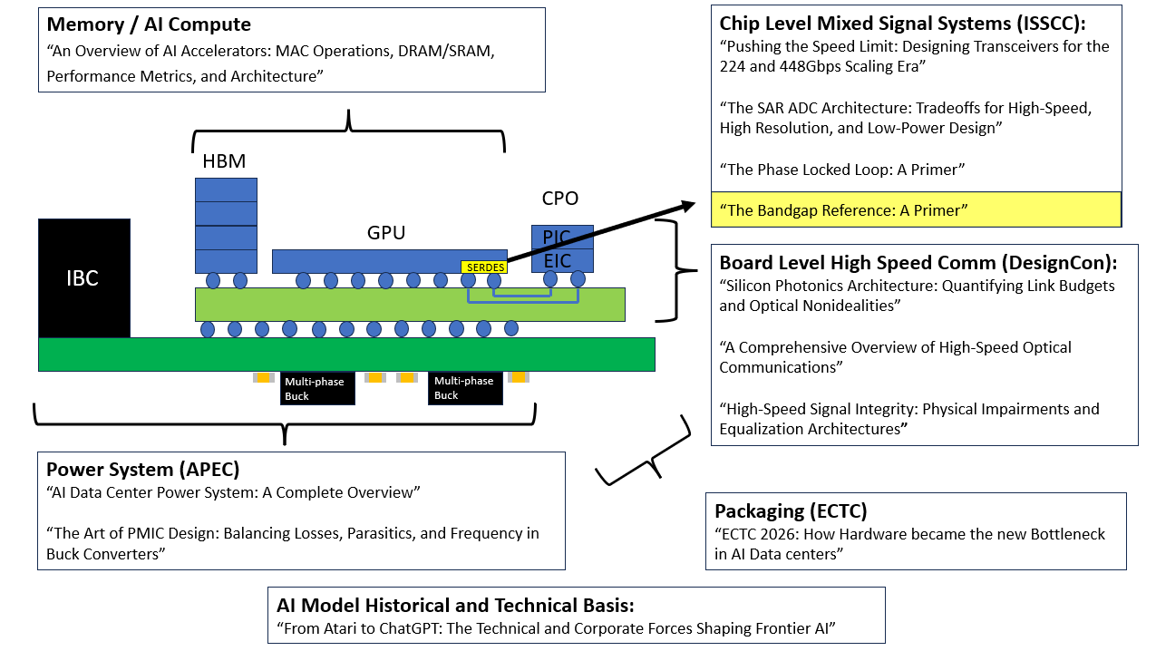
An outline of the deep dives on my Substack “Inside the Silicon Machine”
Editors note (6/1/26) - Moving forward, I am transitioning this Substack into a deep-dive resource on System Architecture that covers the packaging, thermal, power, and signal integrity stack. I added links to additional posts I wrote that interface with Bandgaps after I originally wrote this one. To reflect the depth and combination of the synthesis involved, the deepest technical layers of my guides will now be reserved for paid subscribers.
However, I’ll leave this post free to get a flavor for the type of depth I go into.
A bandgap reference generates a stable voltage with low sensitivity to temperature, supply, and process (often with trimming).
Most IC datasheets specify that the IC will work within a specific temperature range (such as -55 °C to 125 °C). Variations in temperature can shift bias points and thresholds enough to break specs without a stable reference and proper matching.
Bandgap references are found in virtually all analog circuits as stable references for high-precision analog functions, such as ADCs, DACs, and comparators. They are also used to bias current mirrors for setting bias points so that the resulting circuit is robust to PVT variations. Because of their ubiquity, they tend to be reused and modified depending on the fab process and the level of precision required.
Bandgaps look simple, but are a delicate balance of a few fundamental analog principles, including:
- Matching: resistor ratios, BJT area ratios, amplifier offsets
- Feedback: Forcing ΔV_BE and setting I_PTAT robustly
- Temperature variation: How BJT and resistor characteristics vary over temperature, sometimes nonlinearly
- Trim & Calibration: Output accuracy, temp trim, and curvature correction
Below is a self-biased bandgap design example I built that illustrates these principles. I also have a fun side story at the end about how a group of young designers “competed” on who can make the best bandgap.
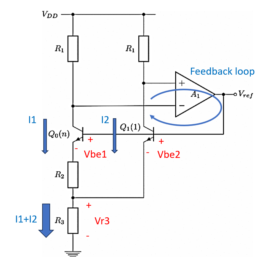
Figure 1. A Brokaw Bandgap Reference with key values labelled
Consider the Brokaw Bandgap reference in Fig. 1. The reference voltage is the output of the op amp. This circuit sums a PTAT voltage and a CTAT voltage:
- A PTAT voltage (Proportional to absolute temperature) means that the voltage increases with increasing temperature.
- The PTAT voltage is generated by the BJT base - emitter voltage difference ΔV_BE = Vt*ln(n) by forcing two BJTs to operate at different current densities (often via an emitter-area ratio n). This voltage appears across R3 in the above example.
- A CTAT voltage (Complementary to absolute temperature) means that the voltage decreases with increasing temperature.
- The CTAT voltage is generated across the base-emitter of the BJT which behaves like a diode. The reason behind this is related to the fact that the bandgap energy of silicon decreases with increasing temperature.
Additionally, the op-amp sets the PTAT current by driving the loop so its input nodes match (in the ideal case).
When both PTAT and CTAT voltages are summed with the right scaling, the first-order temperature dependence largely cancels, leaving a much flatter reference over temperature.
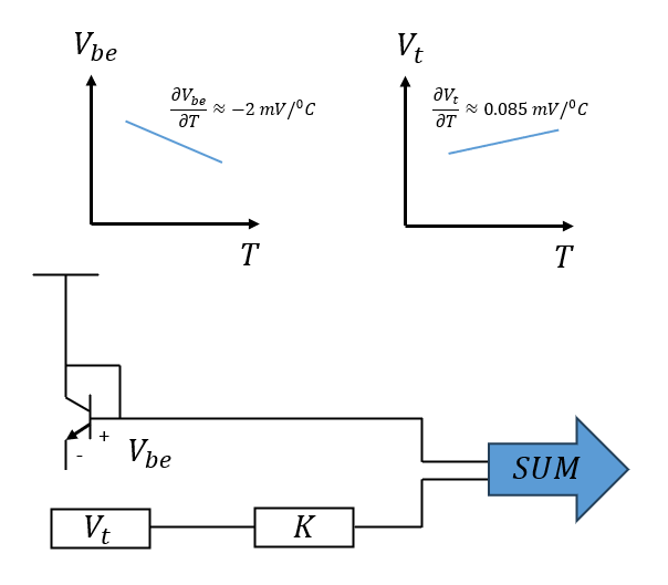
Figure 2. Showing how PTAT and CTAT Voltages sum to cancel each other to generate a temperature-insensitive voltage
Derivation of Output Voltage
The derivation of the output voltage is as follows. Starting from KVL:
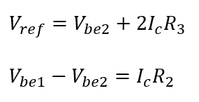
The current through the circuit flows through R2, where the voltage across it is the difference of the base-emitter voltages of Q and Q1:
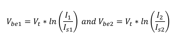
Is is the saturation current of the diode. Substituting all of the terms:
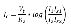
The op amp uses negative feedback to ensure that I1=I2, so both terms can be cancelled. However, Is1 and Is2 are proportional to the cross sectional area of the BJT. Therefore,

where n is the number of BJTs in parallel for Q0. The output voltage is given by:

The output voltage is the sum of a PTAT voltage (Vt) times a gain term and a CTAT voltage Vbe1. However, the temperature variations are not the same. The temperature variations of each term are:
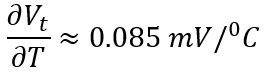
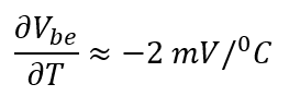
The values in the term R3/R2*log(n) are selected such that the dV/dt of both terms cancel each other:
- n = 8 is common because 8 unit devices plus 1 unit device can be arranged symmetrically (e.g., a 3×3 array) to improve matching.
- The resistor ratio R3/R2 is selected to be equal to 5.5.
Using a bias current of 55 uA and Is1 = 6.734 fA from the SPICE model, and substituting all of these values in the equation above:
- Vbe1 = .59V.
- V ref at 27 °C = 1.18V.
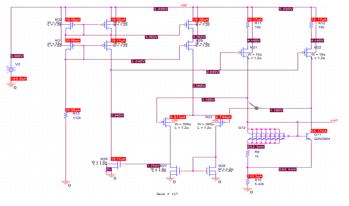
Figure 3. SPICE schematic of a Bandgap reference with amplifier and current biases
The circuit consists of the bandgap core which generates the PTAT and CTAT voltages. Both collector voltages are fed into an op amp which uses a PMOS differential pair as the first stage. This is done to avoid the VMIN problem an NMOS based op amp would experience since the common mode input voltage is approximately 1.18V.
The output of the first stage is fed into a second stage where the output is referenced to the VDD rail to control the PMOS current sources. The op amp is biased with a PMOS based cascode current mirror of 20uA. All of the DC voltages and currents are shown at T = 27 °C.
The simulation results of the bandgap reference are shown below.
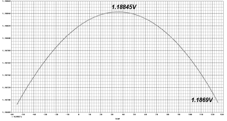
Figure 4. Output Voltage across Temperature
Output voltage across temperature. The graph above shows the DC value of Vref as temperature swept from -55 °C to 125°C in 1°C increments. Ideally, the voltage should be flat across temperature, but the simulation shows the voltage follows a parabolic shape. The maximum voltage is 1.1885V which occurs at approximately 30 °C. The voltage drops for lower and higher temperature, where the minimum voltage is approximately 1.1869V. When the voltage is confined to this range, the maximum voltage difference is 1.6 mV, which is a variation of 0.14% over temp.
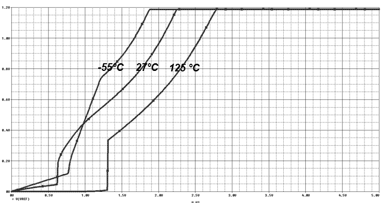
Figure 5. Line Regulation
Line Regulation. This simulation sweeps the value of the voltage supply for three different temperatures: -55 °C (left curve), 27°C (middle curve), and 125 °C (right curve). The reference voltage stabilizes when the power supply has reached a certain threshold. This threshold is different for all three temperatures and is shown in Table 1. Once the power supply voltage has reached its threshold, the reference voltage is fairly stable.
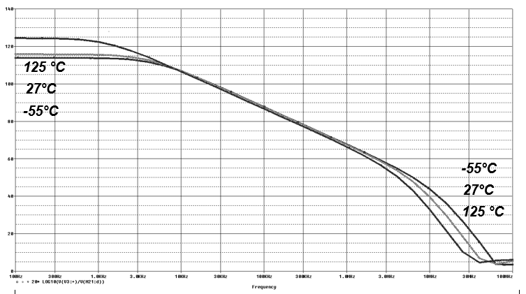
Figure 6. PSRR across Frequency
Power supply rejection ratio, or PSRR. The PSRR is the ability for the circuit to reject noise from the power supply. It is defined as:

To perform this simulation, an AC signal of 1 mV was places in series with the power supply voltage. An AC sweep was performed for three temperature values from 100Hz to 100MHz and the magnitude of the output voltage was observed. The above formula was then applied to obtain the plots shown above, with results shown in table 1.
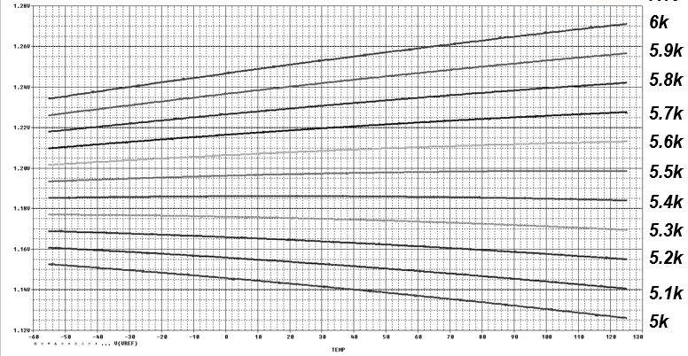
Figure 7. Output Voltage across Mismatch
Mismatch in R10 Resistor. The resistance was swept parametrically from 5kΩ and 6kΩ in 100Ω increments and the output voltage is plotted. This simulation shows that for low resistor values, the CTAT voltage of the BJT dominates the characteristic, and the curve drops over temperature. When R10 is high, the PTAT voltage dominates, and the reference curves increase over temperature.
The following chart summarizes the simulation results.
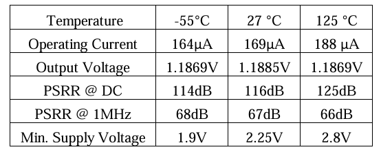
Table 1. Bandgap Simulation Results
There are additional features that bandgaps need:
Trim Range. The degree to how precise a bandgap has to be depends on the precision required across PVT. Monte carlo simulations are run to determine the untrimmed range over which the output voltage can vary, and trim features are added in appropriate places to ensure the output voltage can be turned to within spec across the temperature range.
Curvature Correction. Parts that operate in wide temperature ranges with tight specs can require additional “curvature correction” to improve the error across temperature. First order cancellation like resistor-only tuning can give residual curvature because parameters can have nonlinearities across temperature (such as BJTs) that affect the output.
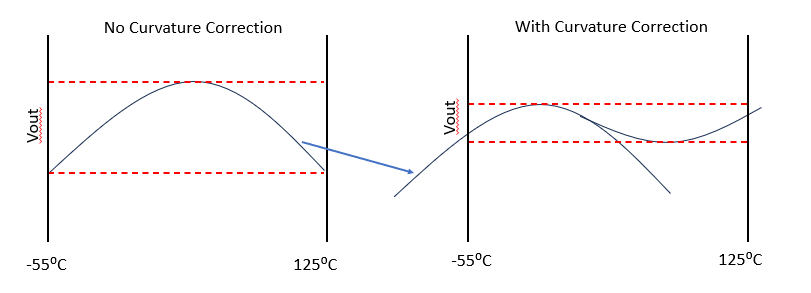
Figure 8. Curvature Correction of a bandgap by modifying PTAT, CTAT curves and adding a nonlinear component to the circuit to improve accuracy over temperature.
Startup Circuitry. Because the core is self-biased, it has a zero-current equilibrium point, so startup circuitry is required to guarantee the intended operating point.
At an Analog Design internship, I once saw a group of young engineers have a friendly completion against each over who can design a bandgap with the highest accuracy across temperature. Work was to be done after 2-3pm on Friday so as to not interfere with day to day work.
Most of the “tricks” they experimented with involved:
- curvature correction techniques, like how to bias a transistor to turn on as a specific temperature, and where to place in the circuit
- NPN / PNP topologies
- value ratios (n, resistors)
- what current mirror to use (cascode, wide swing, source degenerated, wilson)
- what amplifier topology (NMOS, PMOS, gain stages, active loads) maximize gain and minimize offset
Each participant presented their results weekly and learned insights from each other to improve their day job, since analog is an art after all.
I feel like designing bandgaps are a really good introduction to analog circuit design because designing them develops a lot of the fundamentals used in more complex analog circuits.
第二部分:解析(深度解读)
一、核心论点摘要
带隙基准源(Bandgap Reference, BGR)是所有高精度模拟电路的「定海神针」:它产生一个对温度(Temperature)、电源(Supply)、工艺(Process)都几乎不敏感的稳定电压,是 ADC、DAC、比较器以及偏置电流镜的参考源。这篇文章用作者自己搭的一个自偏置 Brokaw 带隙为例,把「PTAT+CTAT 一阶温度抵消」的物理直觉、数学推导、SPICE 仿真(温漂、线性调整率、PSRR、失配)以及工程上的「曲率校正 / 修调 / 启动电路」三件套讲了一遍,最后还分享了一段模拟工程师之间「谁做的带隙最准」的趣味竞赛。
二、关键概念解读
1. PTAT 与 CTAT:一正一反,凑出一个温度无关量
- CTAT(Complementary To Absolute Temperature):BJT 的 V_BE 随温度升高而下降(约 -2mV/°C),本质上是硅的带隙能量随温度升高而减小。
- PTAT(Proportional To Absolute Temperature):利用两个不同电流密度的 BJT,其 ΔV_BE = V_t·ln(n) 随温度升高而上升(V_t = kT/q 与绝对温度成正比,n 为发射极面积比)。
- 把两者按正确比例相加,一阶温度系数两两抵消,得到一条在温区里相当平坦的曲线——这就是「带隙基准」名字的由来(目标电压 ≈ 硅带隙电压 1.2V 量级)。
2. Brokaw 结构的核心 运放通过负反馈强制其两个输入节点等电位,从而 I1=I2,使 ΔV_BE 精确落在 R3 上,并设定 PTAT 电流 I_PTAT。运放第一级用 PMOS 差分对(而非 NMOS),是因为共模输入电压约 1.18V,NMOS 输入对会撞上 VMIN 问题。偏置用 20μA 的 PMOS cascode 电流镜。
3. 数值取向(行业惯例)
- 面积比 n=8:8 个单位管 + 1 个单位管可排成对称的 3×3 阵列,极大改善匹配(matching)。
- 电阻比 R3/R2 = 5.5,配合 ln(8) 让一阶 dV/dT 抵消。
- 代入 55μA 偏置、SPICE 模型 Is1=6.734fA,得到 Vbe1≈0.59V,Vref(27°C)≈1.18V。
4. 三个必须正视的非理想项
- 曲率校正(Curvature Correction):电阻-only 的一阶抵消在宽温、紧指标下会残留二阶抛物线误差(BJT 的 V_BE 随温度有非线性),需要额外加入非线性分量把曲线「拉平」。作者仿真里 Vref 在 -55~125°C 呈抛物线,最大 1.1885V@~30°C、最小 1.1869V,温漂仅 1.6mV(0.14%),已经相当不错。
- 修调范围(Trim Range):PVT 下未经修调的输出会散开,需跑 Monte Carlo 仿真确定散开范围,再在合适位置加数字修调位把输出「拧」回规格内。
- 启动电路(Startup):自偏置核心存在零电流平衡点(全 0 也是平衡解),必须靠启动电路把电路「踢」进正常工作点,否则上电后可能停在死区。
5. 其他关键指标(仿真印证)
- 线性调整率(Line Regulation):电源扫到某个阈值后 Vref 才稳定,且 -55/27/125°C 三个温度的阈值各不相同(见表 1)。
- 电源抑制比(PSRR):在电源上串 1mV AC、100Hz~100MHz 扫频,看输出纹波被衰减多少——模拟电路的「抗电源噪声能力」。
三、分层拆解表
| 层级 | 关键模块 | 设计要点 | 非理想性 / 对策 |
|---|---|---|---|
| 物理层 | BJT 对、电阻 | 面积比 n=8、R3/R2=5.5 | 匹配、面积对称排布 |
| 抵消层 | PTAT + CTAT 求和 | ΔV_BE 落在 R3、I1=I2 | 运放失调→负反馈强制等电位 |
| 偏置层 | PMOS 差分对 + cascode 电流镜 | 规避 VMIN、20μA 偏置 | 共模输入 1.18V 限制拓扑选择 |
| 精度层 | 修调 / 曲率校正 | Monte Carlo 定范围 | 二阶抛物线误差、数字修调位 |
| 系统层 | 启动电路 | 脱离零电流平衡点 | 防上电死区 |
四、技术趋势与产业视角
- 模拟是「手艺活」:作者那句「analog is an art」并非客套——曲率校正里「在哪个温度让某个晶体管导通、放在电路何处」这类 trick,靠的是工程师之间的周会分享与试错,很难完全教科书化。
- 基准源是系统级芯片的隐藏地基:光通信(光模块 DSP/驱动器偏置)、SerDes(收发器内部 ADC/DAC 参考)、PLL(压控振荡器偏置)全都依赖稳定的带隙基准。本站已发的 高速光通信入门、信号完整性入门、PLL 入门、SerDes 系统架构拆解 在物理层/模拟层大量用到这类基础模块——本文正好补上「最底层的参考电压从哪来」这一环。
- 从免费到付费的转折:作者 6/1/26 的编者按明确说,后续将把最深层的技术拆解改为付费,但本文保留免费。这意味着同一个 Substack 里,越往后越难通过公开渠道完整获取,发布时需留意付费墙标注。
五、与本站其他文章的连接
- 高速光通信入门 — 光模块里的模拟前端同样依赖稳定偏置。
- 信号完整性入门 — 高速链路中的 ADC/DAC 参考电压即来自带隙。
- PLL 入门 — 压控振荡器与电荷泵的偏置都靠基准源。
- SerDes 系统架构拆解 — 224/448Gbps 收发器的模拟前端以带隙为地基。
- 光投资地图 v1.0 — 模拟/混合信号 IP 是半导体国产化的重要赛道。
六、风险提示
本文为技术科普与原理拆解,不构成任何投资建议。半导体与模拟 IP 领域的投资决策请结合产业供需、公司基本面与自身风险承受能力独立判断。