High-Speed HBM5 Interconnect — 高速 HBM5 互连的信号完整性与协同设计挑战
整理自 Silicon Co-Design(Chad):基于 SK hynix 与 KAIST 的 ECTC 2026 论文,拆解 HBM5 迈向 20-30 Gb/s 时传输线效应显现、1000+ 并行 I/O 无法端接、PSIJ 挤压抖动预算的协同设计难题。英文原文(免费部分)+ 中文深度解读;🔒 付费段未包含。
本文整理自 Silicon Co-Design(作者 Chad,Substack 技术专栏),原文发布于 2026-07-15。 标题原文:A Comprehensive Deep Dive into High-Speed HBM5 Interconnect: Signal Integrity and Co-Design Challenges(URL slug 为
a-comprehensive-deep-dive-into-high)。 结构为 正文(英文原文)+ 解析(中文深度解读),方便中英对照阅读。 ⚠️ 本文为付费专栏。公开免费部分止于「How SK Hynix must incorporate transmission line effects…」一节开头;🔒 付费段(Fundamentals of Transmission Lines、RC 与 LC 两个工作区、echo jitter 的 DoE 结果、KAIST UCIe 的 SI/PI 协同分析框架、PSIJ 量化计算、BONUS「The Brain」3D 定制 HBM)位于付费墙之后。本发布未包含任何付费内容。 文中 11 张配图均在免费段内,已解码为 S3 直链嵌入。
第一部分:正文(Original Article)
A Comprehensive Deep Dive into High-Speed HBM5 Interconnect: Signal Integrity and Co-Design Challenges
How transmission line effects and power-supply induced jitter make high-speed HBM interconnect scaling one of the most challenging co-design issues in AI racks
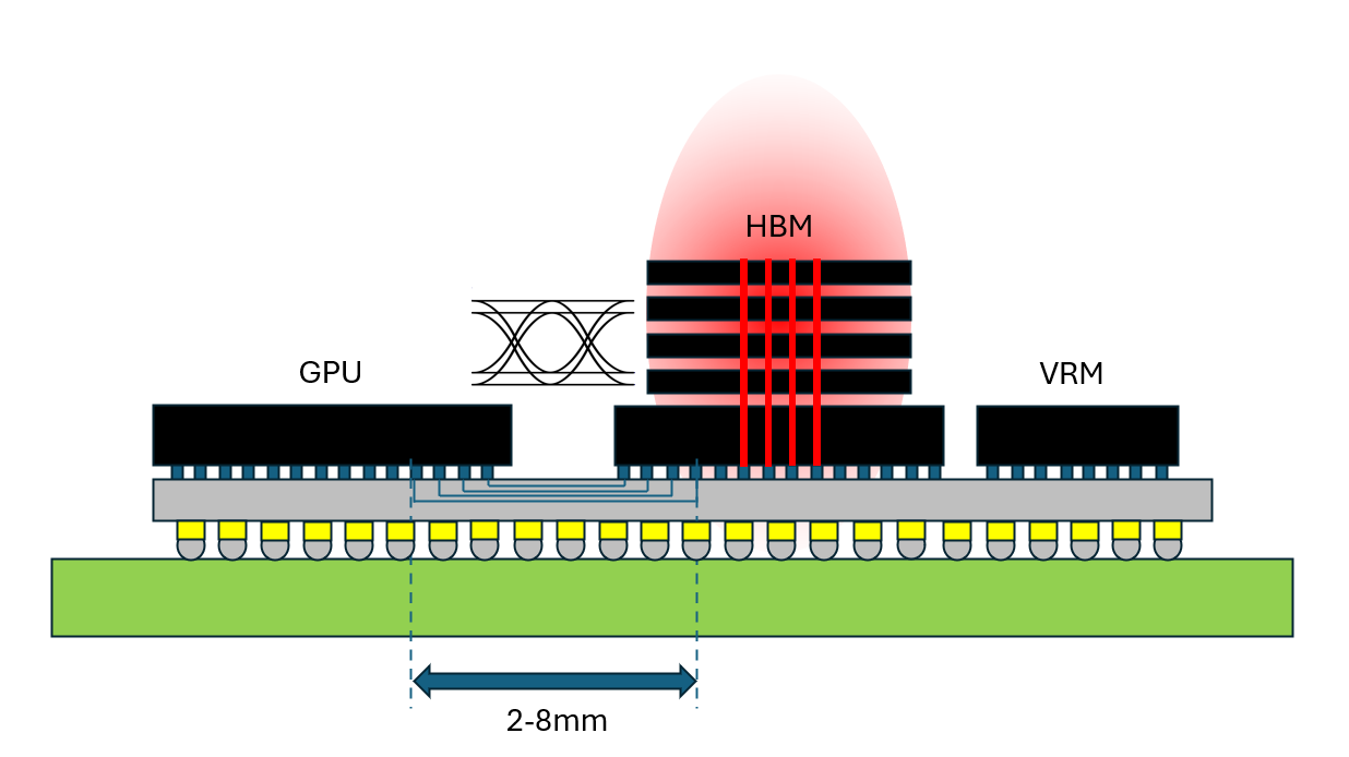
While a lot of attention is being drawn to the current HBM4 shortage, this post will focused on the practical technical challenges in scaling HBM5 performance.
I will discuss the following signal integrity and **co-design **challenges in HBM5 based on SK Hynix and KAIST’s ECTC 2026 papers:
Introduction to Signal Integrity trends from HBM1 to HBM5
Jitter component tree and descriptions of key sources of jitter for short, high-speed interconnect:
Echo
SSC / SSN
PSIJ
How SK Hynix quantifies transmission line effects in high-speed HBM5 data lines
🔒Fundamentals of Transmission Lines
🔒Proposal for two operating regions: RC and LC dominated regimes
🔒Design of Experiments results for echo jitter across interconnect lengths and dimensions
🔒KAISTs SI/PI co-analysis framework for Chiplet (UCIe)-based GPU-HBM Interconnect for PSIJ
🔒Shoreline density limitations for a 4 layer wide-IO and chiplet interconnect scheme
🔒Calculating power-supply induced jitter (PSIJ) from SI, PI, SSC, and jitter sensitivity / amplification
🔒BONUS: “The Brain” - 3D Custom HBM and current status among TSMC, SK Hynix, NVIDIA, and Samsung from ECTC 2026
This post is heavily influenced by the ECTC session 11, “Signal Integrity Design for High-Speed Interfaces” as well as my experience at DesignCon 2026 I was personally in attendance for.
This will be more of an advanced deep dive, but** grounded in fundamentals**. I structured the post to start with baseline EE concepts and building a framework to understand the complexity of multi-layer SI/PI co-design. I have a post that covers the fundamentals of signal integrity that forms the foundation of the issues I discuss:
I encourage you to read through my backlog of knowledge and challenge you to take away one new in-depth concept. Even if the technical material doesn’t stick, I still hope you come away with an appreciation of the challenges that keep HBM and SI engineers up at night.
Note that I am not a signal integrity person. However, I immersed myself into the SI world by attending DesignCon 2026 with an **RF / Microwave lens **upon which to analyze high-speed signal integrity effects. It was clear upon reading these papers that memory and SI engineers do not speak the same language as RF people do, but they describe the same effects from their point of view.
I personally think that at increasingly faster data rates, there will be a convergence of the knowledge among RF / microwave and signal integrity domains. I aim to bridge this gap of understanding.
SK Hynix - High speed HBM roadmaps
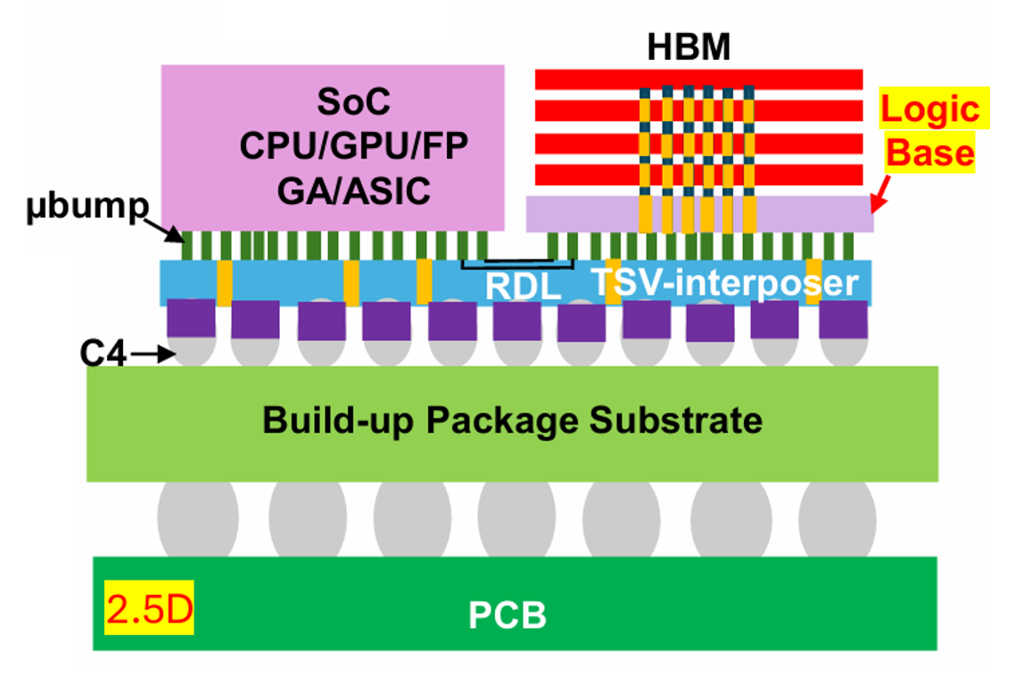
**Figure 1. **HBM used in 2.5D Packaging. Source: J. Lau. “Advanced Packaging for Chiplets, Heterogeneous Integration, and Co-Packaging Optics” ECTC2026
High bandwidth memory (HBM) is a critical component for AI training workloads that stores everything involved in AI computation from model weights, gradients, optimizer states, and activations. HBM connects multiple DRAM dies vertically using TSVs to maximize memory density in the given footprint. These DRAM dies are placed as close to the GPU as possible to maximize the data throughput to overcome the Von-Neumann bottleneck.
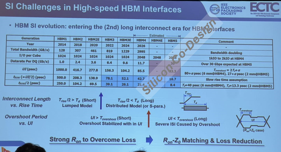
Figure 2. SI Characteristics in Scaling HBM from Gen 1 to Gen 5. Source: T. Bae et al. “Figures of Merit to Characterize the Signal Integrity Performance of Interposer Interconnect for High Bandwidth Memory (HBM)” ECTC2026
In this SK Hynix roadmap presented at ECTC 2026, there are a few performance scaling trends along HBM generations:
Between HBM1 and HBM4, the datarate per DQ increased linearly from 1Gb/s to 11.7Gb/s
Along those generations, the signal rise time and unit interval (UI) scaled inversely proportional to the total data rate per DQ
Between HBM3E and HBM4, there is a stairstep jump in the the total bandwidth by 2.5x, primarily driven by doubling I/O per cube from 1024 to 2048.
To keep with up AI workload demands, HBM5 expects a 20-30 Gbps per DQ range using state-of-the art interposer technologies such as the Chip-on-Wafer-on Substrate (CoWoS-L and CoWoS-R).
At those data rates, HBM is running into co-design challenges along the signal integrity, power integrity, and thermal domains. At ECTC, there are three high-level trends I noticed amongst three papers:
Jitter due to Transmission Line Effects
SK Hynix notes that significant transmission line effects were not observed for previous HBM generations with a data rate of under 10 Gbps per DQ and approximately 6-mm-long interposer interconnects.
However, at 30Gbps rates, advanced packaging interconnect technologies exhibit distinct lossy transmission line characteristics and must be accounted for.
Normally, transmission lines are terminated with equivalent impedances to avoid reflections. However, termination resistors cannot be reasonably employed for terminating 1000+ I/O in HBM as this would lead to** high thermal penalties and static power dissipation**. This leads to additional signal integrity challenges that will be discussed.
From “Wide-and-slow” to UCIe
Another challenge is edge density limitations of I/O. Doubling the number of I/O pins results in excessively large physical layer (PHY) footprint on the silicon. The number I/O is fundamentally constrained by the metal pitch, # of layers, and the area dedicated to ground rails to control crosstalk.
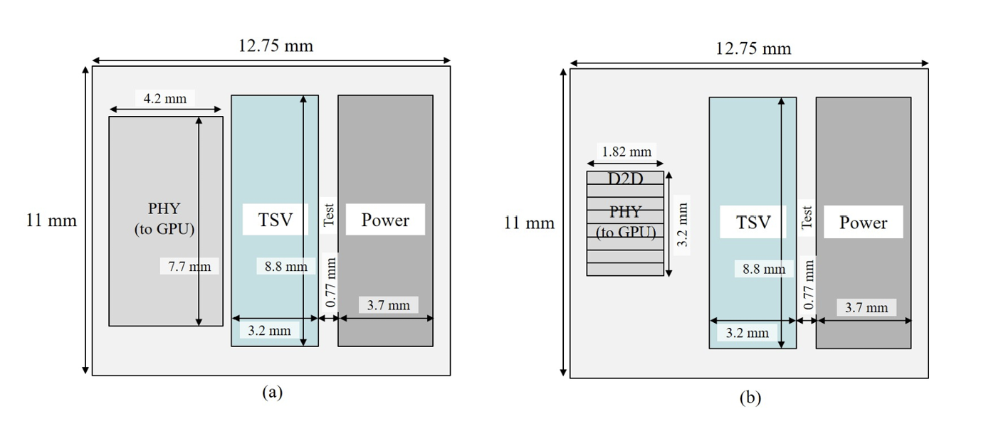
**Figure 3. **An illustration of the shoreline for HBM4 with conventional (and G2D module. Source: H. Suh. “Signal and Power Integrity Co-Analysis of Chiplet(UCIe)-based GPU-HBM Interconnect for Reduced PHY Area” ECTC2026
To scale the number of I/O, KAIST is investigating the performance impact of going from wide-and-slow I/O toward higher-speed SerDes lanes in Universal Chiplet Express (UCIe) standards.
KAIST notes that in chiplet-based GPU-HBM based on UCIe, eight D2D modules are utilized, with each module consisting of 64 Tx and Rx at 32Gb/s each. A total of 512 Tx and Rx supports 2 TB/s for read and write directions.
With a faster, more compact PHY, more I/O them can fit in the HBM shoreline to increase the data throughput.
PDN for 3D stack
Another co-design challenge is how the TSVs in the HBM stack affect thermal characteristics.
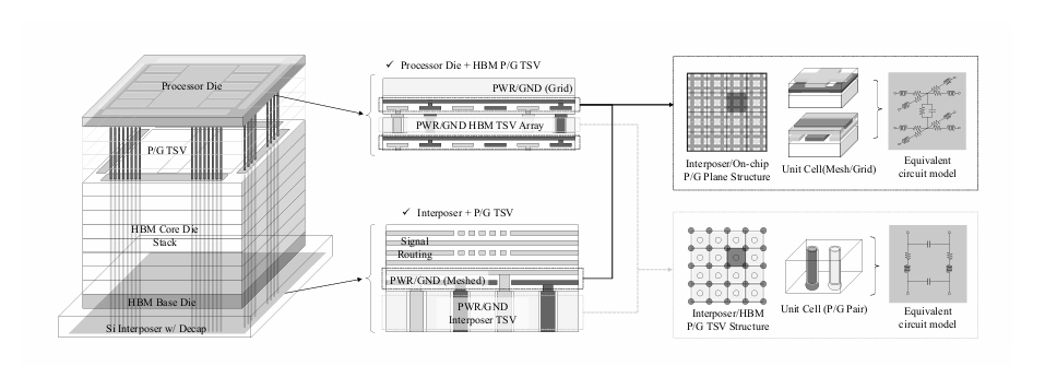
Figure 4. An Illustration of TSVs and the power grid structure used. Source: J. Yoon et al. “Power Distribution Network (PDN) Design and Analysis for Multi-Stack 3D Heterogeneous Integrated High Bandwidth Memory (3D-HI-HBM) Module” ECTC2026
This paper evaluates the thermal and IR drop characteristics of different TSV configurations. Here we see how each component is modelled as an array of unit cells in a grid structure with an equivalent RLC circuit model.
Though I think this paper is important for effective co-design, especially when it comes to modelling PDNs for PSIJ, I have left the analysis out of this post for now to focus on signal integrity challenges from the first two papers.
Key sources of jitter in high-speed, low-voltage parallel lines
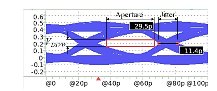
**Figure 5. **A eye measurement for HBM showing aperture and jitter. Source: T. Bae et al. “Figures of Merit to Characterize the Signal Integrity Performance of Interposer Interconnect for High Bandwidth Memory (HBM)” ECTC2026
Jitter is a key constraint of high speed signal integrity and must be accounted and minimized as much as possible.
When high speed data is sent to and from the HBM, each bit is received within a given time slot refers to as the “Unit Interval” (UI) or Bit-period. Jitter and slew rate constraints reduce this to an effective aperture “window” where data can be received. Throughout the post, all aperture results are normalized to a UI of 1.
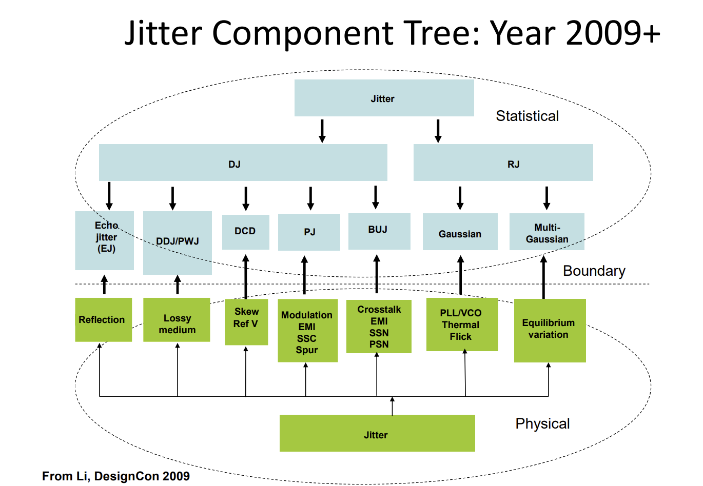
**Figure 6. **Jitter component tree showing both the statistical effects of jitter and the physical mechanics that cause them. Source: M. Li. “Design and Verification for High-Speed I/Os at 10 to 112 to 224 Gbps, and 448 Gbps with Jitter, Signal Integrity, and Power Optimized” DesignCon 2026
There are many difference sources of jitter as shown in this comprehensive jitter tree from Dr. Mike Peng Li’s DesignCon 2026 tutorial slides.
Jitter is broken down into two main statistical categories: deterministic and random jitter. I describe these in more detail, along with equalization techniques, in the following post:
Under deterministic jitter, there are three primary classes of jitter relevant to high speed, massively parallel, non-terminated lines:
Echo Jitter - Jitter caused by impedance mismatches and reflections
When a signal propagates down the line and encounters an impedance mismatch, part of the signal reflects backward and forwards, resulting in a stored “memory” and overshoot that affects future bit measurements. This can lead to ISI.
**Bounded Uncorrelated Jitter **- Jitter that is bound but uncorrelated to the signal
This includes** crosstalk **across massively parallel lines where there are many different possible combinations of crosstalk interactions, but the overall jitter impact is “bounded” to worst case conditions.
Periodic Jitter - Jitter where the timing variations repeat in a cyclical pattern over time at a specific frequency
This includes **simultaneous switching noise that occurs **every switching period.
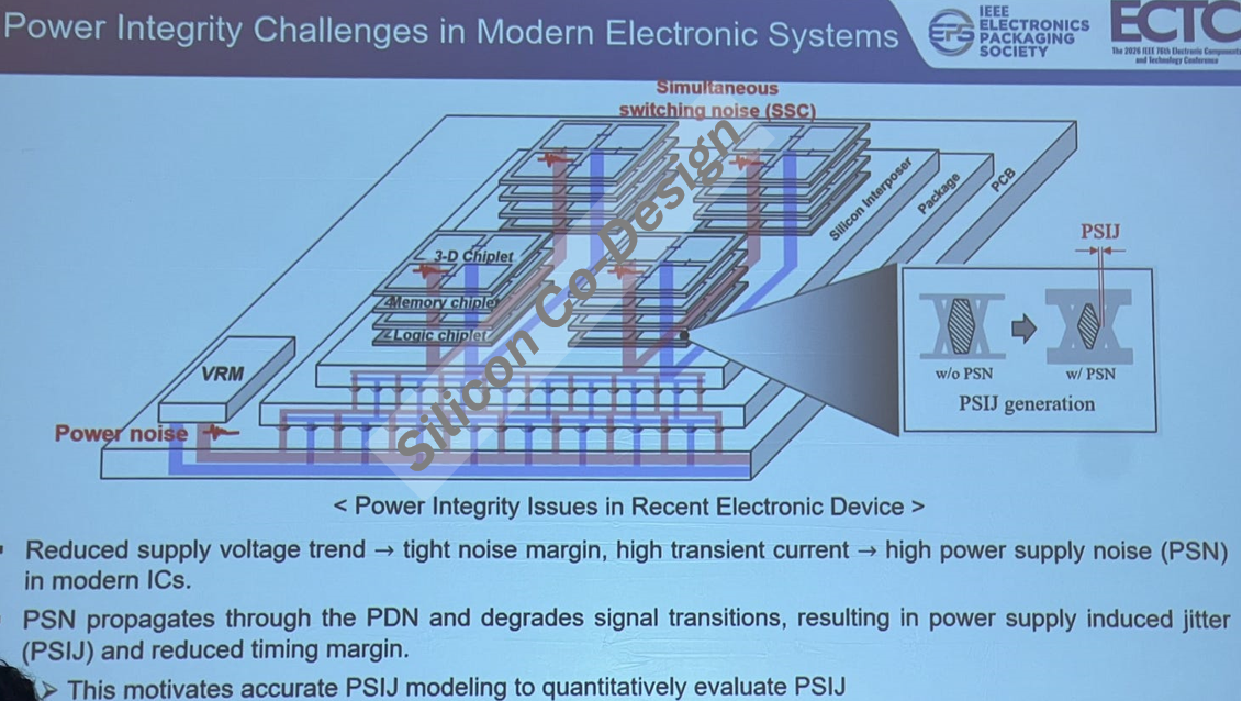
Figure 7. A high level illustration of PSIJ manifesting from power noise from the VRM coupling. Source: H. An et al. “Analytical Approach to Statistical Modeling of Power Supply Induced Jitter” ECTC2026
One source of jitter that is particularly problematic at increasing data rates is** power-supply induced jitter (PSIJ)** which is a form of power-noise-induced timing degradation within circuits themselves. This is a challenge to model because it combines jitter from a few sources.
The rise / fall time and propagation delay of a circuit depends on how quickly FET caps can get charged by the PDN. When gates are switched, they generate simultaneous switching current (SSC) **that go through the PDN and cause **simultaneous switching noise (SSN) on the line. Noise on the PDN can affect the current your caps charge at, introducing **timing uncertainty. **
PSIJ becomes more problematic as you stack and cram more HBM on the same PDN and the PDN line becomes noisier. With increasing data rate, thousands of I/O drivers switching simultaneously, and a low supply voltage, a marginal increase in PSIJ can eat into the jitter budget and lead to signal failures. A co-design approach to modelling PSIJ will be discussed in more detail behind the paywall.
How SK Hynix must incorporate transmission line effects in high speed HBM data lines
Now lets discuss some of the high-speed SI challenges SK Hynix is facing from transmission line effects. I’ll start with a broad introduction of transmission effects from an RF point of view, the nuances as it relates to SI, then jump right into SK Hynix’s analysis after the paywall.
第二部分:解析(深度解读)
核心论点摘要
作者以 ECTC 2026 第 11 分会「Signal Integrity Design for High-Speed Interfaces」与 DesignCon 2026 的一手材料为基础,讨论一个核心问题:当 HBM 单引脚速率从 HBM4 的 11.7 Gb/s 迈向 HBM5 的 20–30 Gb/s,互连不再能被当作「短接线」处理,而变成有损传输线;信号完整性(SI)与电源完整性(PI)必须从各自优化转为协同设计。
三条主线:
- 跨过 10 Gb/s 门槛后传输线效应显现——HBM4 及更早(低于 10 Gb/s、约 6 mm 中介层走线)观察不到显著传输线效应;到 30 Gb/s 则呈现明显的有损传输线特性。
- 1000+ 并行 I/O 无法端接——传统用匹配阻抗端接消除反射的做法,在 HBM 上会因热代价与静态功耗而不可行,于是反射与回波抖动上升为主要矛盾。
- 抖动预算被多方挤压——echo jitter(阻抗失配)、bounded uncorrelated jitter(串扰)、periodic jitter(同步开关噪声)叠加,再叠加 PSIJ(电源诱导抖动);在低电压、数千 I/O 同时翻转的条件下,PSIJ 的边际增长即可吃掉抖动预算。
关键概念解读
1. HBM 代际:带宽靠「速率 × I/O 数」双轮驱动
- HBM1→HBM4:单 DQ 速率从 1 Gb/s 线性提升至 11.7 Gb/s;信号上升时间与单位间隔(UI)随总速率成反比收缩。
- HBM3E→HBM4 出现 2.5× 的台阶式跳变,主因是单 stack I/O 从 1024 翻倍到 2048,而非单纯提速。
- HBM5 目标 20–30 Gb/s per DQ,依赖 CoWoS-L / CoWoS-R 等先进中介层技术。
含义:速率与 I/O 数同时放大,意味着 SI 问题不是线性恶化,而是乘积式恶化——这也是为什么 HBM5 的难点集中在 co-design 而非单点工艺。
2. 为什么「不端接」是 HBM 的关键约束
常规高速链路用端接电阻吸收反射。但 HBM 拥有 1000+ 条并行 I/O:
- 每条都端接 → 静态功耗不可接受;
- 密集端接 → 热密度进一步恶化(HBM 本就紧邻 GPU 堆叠,散热已是瓶颈)。
结果是必须容忍失配与反射,工程问题从「消除反射」转为「建模并预算反射引起的回波抖动(echo jitter)」——这正是 SK hynix 论文的核心内容(位于付费段)。
3. 从 wide-and-slow 走向 UCIe:岸线(shoreline)密度之争
I/O 数量受三个物理量硬约束:金属间距(metal pitch)、可用布线层数、以及为抑制串扰而预留的地线面积。单纯翻倍 I/O 会让 PHY 面积膨胀到不可接受。
KAIST 换了一个思路:不再加宽并行总线,而是改用 UCIe 标准下的高速 SerDes 通道——8 个 D2D 模块、每模块 64 Tx 与 64 Rx @ 32 Gb/s,合计 512 Tx + 512 Rx 支撑 2 TB/s(读与写方向)。本质是用更窄但更快的 PHY,换取单位岸线带宽。
4. 3D 堆叠的 PDN:TSV 不只是信号通道
HBM 用 TSV 垂直串联多颗 DRAM die,而 TSV 同时承担供电,因此它直接影响热特性与 IR drop。文中引用的论文把 TSV 与电源网格建模为单元阵列(unit cell grid)加等效 RLC 电路——这是把「物理结构」转成「可仿真电路」的标准手法,也是后续建模 PSIJ 的基础。作者明确把这部分分析留到付费段,本文只保留其建模思路。
5. 抖动分类:一张树状图看懂
抖动先分为确定性(deterministic)与随机(random)两大类。针对高速、大规模并行、无端接的 HBM 链路,免费段聚焦三类确定性抖动:
| 抖动类型 | 物理机理 | 典型来源 |
|---|---|---|
| Echo Jitter(回波抖动) | 阻抗失配使信号前后反射,形成「记忆」与过冲,可导致码间干扰 ISI | 未端接的短互连、过孔与介质界面 |
| Bounded Uncorrelated Jitter(有界不相关抖动) | 与信号本身不相关,但存在明确上界 | 大规模并行线之间的串扰 |
| Periodic Jitter(周期性抖动) | 定时偏差按固定频率周期性复现 | 每个翻转周期的同步开关噪声(SSN) |
6. PSIJ:把「电源噪声」翻译成「时间误差」
这是全文最值得记住的因果链:
- 门电路翻转 → 产生同步开关电流(SSC);
- SSC 流经 PDN(含寄生阻抗)→ 产生同步开关噪声(SSN);
- PDN 噪声改变 FET 栅电容的充电速度 → 改变传播延迟与上升/下降时间 → 产生定时不确定性;
- 最终表现为 PSIJ(电源诱导抖动)。
关键在于低电压 + 大规模并行 + 高堆叠的三重放大:供电电压越低,同样幅度的噪声占比越大;I/O 越多,同时翻转越强;HBM 堆叠越多,共享 PDN 越脏。因此作者强调:PSIJ 的边际增长就能吃掉抖动预算并导致信号失效——这正是「SI/PI 协同设计」这一术语的现实由来。
分层拆解:从物理结构到系统约束
| 层级 | 关键对象 | 约束 | 付费段延伸内容 |
|---|---|---|---|
| 器件/电路 | FET 栅电容充电速度 | 传播延迟随 PDN 噪声漂移,即 PSIJ | PSIJ 的量化计算 |
| 互连(物理) | 中介层走线、TSV | 低于 10 Gb/s 无显著传输线效应;30 Gb/s 呈有损传输线 | 传输线基础、RC 与 LC 两个工作区 |
| 链路(电气) | 1000+ 并行 I/O、无端接 | 反射导致 echo jitter;串扰导致有界抖动 | 回波抖动 DoE(跨互连长度与尺寸) |
| 架构/PHY | shoreline 密度、UCIe | metal pitch、层数、地线面积 | KAIST UCIe SI/PI 协同、4 层 wide-IO 岸线极限 |
| 封装/系统 | 2.5D CoWoS、3D 堆叠 PDN | 热、IR drop、共享 PDN 噪声 | BONUS「The Brain」3D 定制 HBM |
与本站其他文章的连接
本文讨论的 HBM 互连问题,其物理边界是由先进封装决定的——TSV 制造、RDL 工艺、C4/C2 凸点、基板选型在上一篇中已逐一拆解:
先进封装与异构集成完全技术概览(2D→3.5D、CoWoS 拆解)
两篇合读可以理解一条完整链路:封装决定了互连的几何与材料,而这些几何材料参数在 HBM5 的速率下直接转化为抖动与功耗预算。
风险提示与阅读边界
- ⚠️ 付费段未包含:传输线基础、RC/LC 工作区划分、回波抖动 DoE、KAIST 的 UCIe SI/PI 协同分析、PSIJ 量化计算、BONUS「The Brain」3D 定制 HBM 均在付费墙之后。本文只覆盖免费公开部分,未包含任何付费内容;涉及具体数值结论(如 echo jitter 随互连长度的量化结果)请购买原文。
- 作者自述并非信号完整性专业出身,而是以 RF / 微波视角切入,文中判断属二手解读(基于 ECTC 2026 论文与 DesignCon 2026 参会笔记)。
- 文中速率、带宽与配置数据来自 SK hynix、KAIST 的 ECTC 2026 论文及 J. Lau 的报告,属特定时点的公开材料;HBM5 规格尚未最终冻结,量产实现仍可能变化。
- 本文解读部分为基于公开免费段的框架性梳理,不构成任何投资建议。