实地探访 Avicena:MicroLED 互连的真实边界在哪里 —— 单通道 3 Gbps、约 10 米色散上限与「真正的对手是铜」
Vikram Sekar 实地探访 Avicena 后的第一手观察报告(原文为付费文章,本站仅转载公开段):GaN 蓝光 microLED 量产 3–3.5 Gbps、实验室 8 Gbps 仍是自由空间短链路;色散把 reach 锁在约 10 m,因此真正的竞争者是铜而不是光——1–3 pJ/bit 换来三倍于线性有源铜缆的距离。作者反对厂商 30–50 m 的距离宣传。含英文原文公开段(8 张配图)与中文深度解读(含色散量级复核、铜缆 reach 交叉核对与付费墙缺口的结构性影响)。
来源:Viks Newsletter(Substack,半导体行业分析)— A MicroLED Field Trip to Avicena 副标题:What I learned by looking at the tech first-hand 作者:Vikram Sekar(@vikramskr) 原文链接:https://www.viksnewsletter.com/p/a-microled-field-trip-to-avicena | 原文发布日:2026-09-19 | 本站发布:2026-09-21 付费状态:付费文章(
audience = only_paid)。本站仅转载公开段——对象清单、Lane Rates、Reach 三节(含 8 张配图);付费段(串扰与抖动、Gearbox、物理构造与制造、结论)未含,中文解读中已专节说明该缺口对结论的影响。 立场提示:作者声明本文无赞助;Avicena 审阅了草稿以核对事实,作者保留编辑独立权。文中两张量化图来自作者自家 SemiExponent 的估算与数据库,不是第三方实测。文首目录中的「Paid section」条目为原文所有,原样保留以便读者知悉墙后内容。 本页内容:第一部分为英文原文公开段转载(版权归原作者,仅调整排版层级、剔除站点订阅推广段);第二部分为独立撰写的中文深度解读,其中带质疑、重算与补强的判断属解读者观点。
第一部分:正文(Original Article / 英文原文 · 公开段)
While I was in the Bay Area last month attending Hot Chips, I asked Avicena if they would host me for a few hours and show me around their facility, and more specifically, show me their MicroLED technology. They graciously agreed.
I was particularly interested in seeing microLED tech first hand because there has been a lot of debate whether microLEDs are a viable interconnect technology in the datacenter. My purpose was to ask as many questions as I can, to see if I can make sense of whether standard objections to this technology hold up, and allow people actually building this technology to give their account first hand instead of simply inferring from papers, conferences, or opinions.
Most impressively, the entire top brass of the company – from their CEO, Marco Chisari, to the entire senior management of the company in charge of various parts of the business – hosted me and discussed various aspects of their technology. What follows in this report is my observations from the visit mixed in with my own research and opinions of where I think microLEDs are going.
Disclaimer: This article is not sponsored by anyone. The only ‘compensation’ was the bubbly water I drank at Avicena. Not that they did not have other stuff to offer, I just wanted bubbly water. My goal is to provide a neutral, factual account of where this technology is headed while being as informed as possible. If I got something wrong, reply to this email and let me know. This stuff is complex.
Avicena reviewed a draft of this article for factual accuracy. I retained editorial independence.
What’s in this article
Free section:
- Common objections and claimed benefits of microLED interconnects: lane rates, reach, fiber count, jitter, crosstalk, gearboxing
- Lane rates: where Avicena’s production microLEDs run today (3 to 3.5 Gbps), the 8 Gbps next-gen device I saw in the lab, and why there is no roadmap to catch microVCSELs on per-lane speed
- Reach: why chromatic dispersion caps microLEDs at about 10 m, why the real competitor is copper and not laser optics, and what a 300+ lane cable looks like at 5 m
Paid section:
- Crosstalk and jitter: victim/aggressor bathtub measurements on a live LightBundle link, with aggressors on and off, same and different PRBS patterns, and what the results say about signal integrity at 3 Gbps
- Gearboxing: what 64:1 versus 4:1 ratios actually cost in chip design, clock forwarding, deskew, and whether gearboxing can be removed entirely
- Physical construction and manufacturing: the transmit/receive chip, solder ball microLED integration on 300 mm wafers, molded lens arrays, fiber bundle alignment and connectors, the in-house Aixtron reactor, and the path to volume
- Concluding thoughts: the 30 m reach question, redundancy and temperature behaviour, the customer scale-in request, and where microLEDs fit against copper at 1.6 Tbps
Common Objections/Benefits to MicroLED Technology for Interconnects
A framework I had while going into this, was to deliberately list out why people think MicroLEDs will not work for interconnects and try to address it during my visit. Here is a list of common objections:
- Lane rates: MicroLEDs are too slow on a per-lane data rate basis and scaling to higher lane rates is hard.
- Poor reach: The linewidth of microLED light is poor, and chromatic dispersion in the cable will ultimately limit its reach. 10 meters or below is believable, but 30 meter reach at good BER is a stretch.
- Fiber count and alignment: A consequence of (1) is that too many fibers are required to get the lane rates to any meaningful speeds. Adding fibers is not a scalable solution. Cable itself gets bulky. Aligning hundreds of fibers to the array of microLEDs is difficult to do, especially at scale.
- Jitter: MicroLEDs are very noisy, cause a lot of jitter and degrade the bit error rate (BER).
- Crosstalk: Bundling 100s of fibers together means that there is a lot of crosstalk. Not too many critics clarify what they mean by crosstalk. There are two kinds: (1) between optical fibers carrying light, and (2) between different electrical lanes at the two ends of the cable that have to feed the hundreds of lanes.
- Gearboxing: The SerDes on the IC side provides 8x200G lanes, for example. Converting this to say 400x4G lanes requires a gearboxing chip that is difficult to do.
The benefits stated for microLEDs are low power, low cost, better thermal performance, better availability compared to lasers, high bandwidth densities, simple silicon integration and more reliability stemming from redundant links in the array.
We’ll discuss these in detail next.
Lane Rates
Avicena’s microLEDs are built on GaN technology, and emit blue light in the 420 to 440 nanometer wavelength range. Their current production process has a data rate of 3-3.5 Gbps per microLED. The chart below shows the evolution of data rates in microLEDs across industry and academia. These are raw lane rates only, with no consideration for reach or BER.
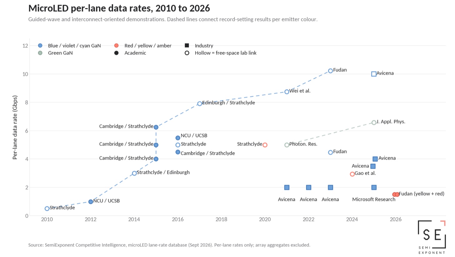
Avicena’s next gen microLEDs are still in the lab, but I got a chance to see it in action running at 8 Gbps. The important thing to understand is that this speed is not through fiber, but instead a very short free space link in a lab. Think about shining the microLED right into the detector kept a really short distance away. This approach removes the impact of the optical fiber and shows just the data rate of the microLED. Here are some pictures I took.
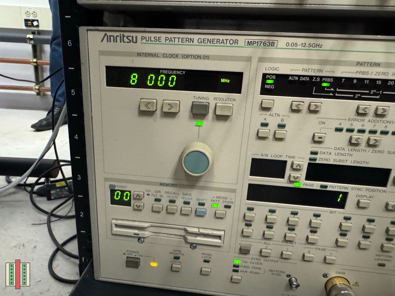
Here is the pulse pattern generator running at 8 GHz.
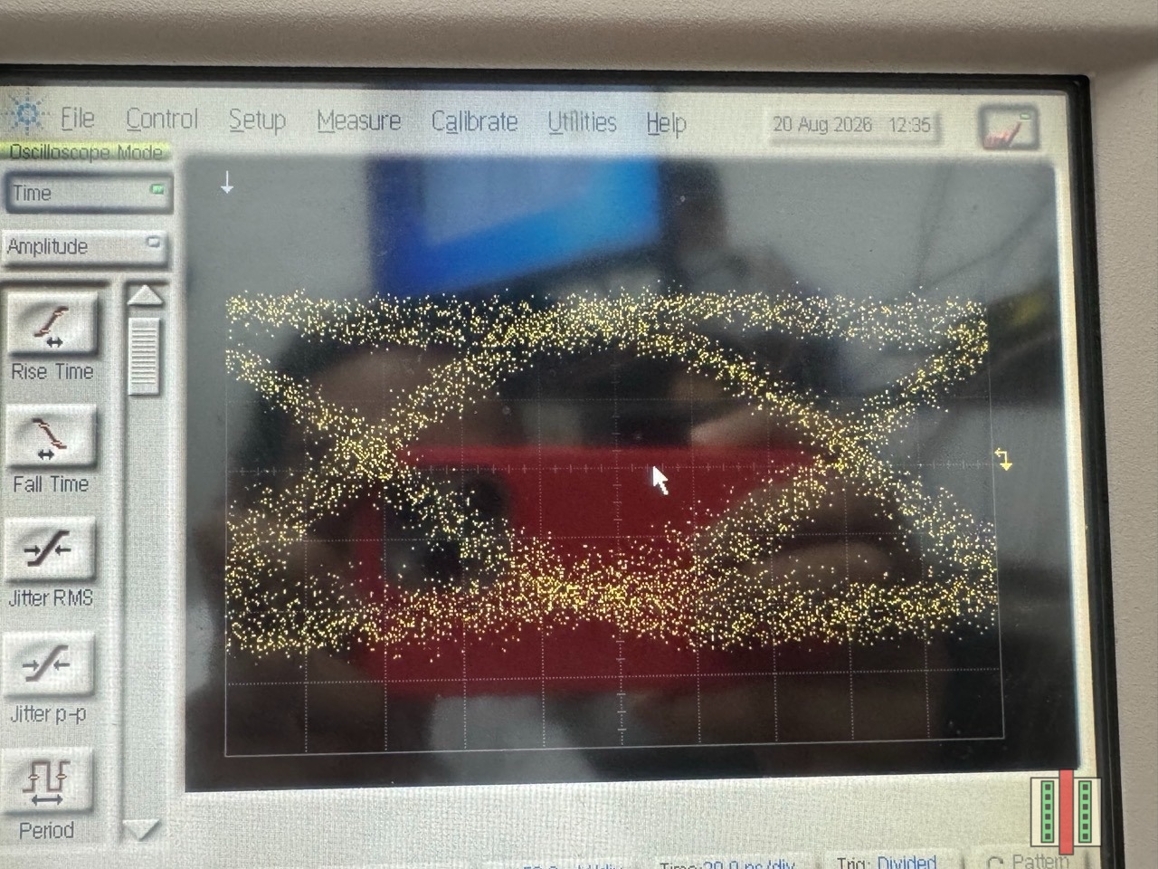
The eye-diagram from the scope runs an NRZ TX-RX short link over free space, which looks pretty clean. Jitter is quite low, and the eye is wide open.
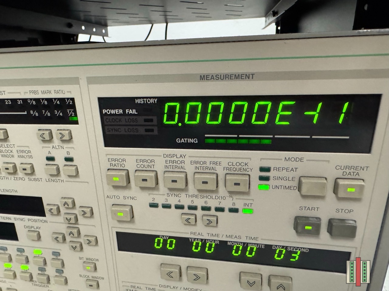
The BER measurement shows better than 1e-11, which signifies that the eye is clean. Again, there are no channel impairments here and the results are free of chromatic dispersion which will limit reach at good BER.
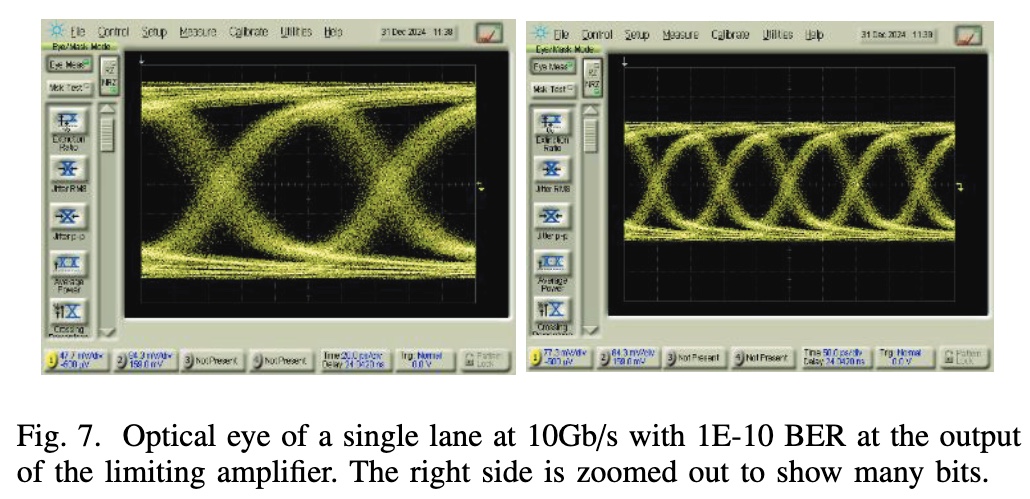
In the chart above, the Avicena data point showing 10 Gbps is an interesting one (doi: 10.1109/LPT.2025.3552708). In this work, they drove the microLEDs with an external driver circuit instead of an integrated one, and were able to show bit rates of 10 Gbps per lane, with 1-e10 BER. Avicena also stated that they’re developing a next generation optical engine that will support 8 Gbps links with LEDs and PDs integrated onto a new ASIC.
The landscape of microLEDs says that lane rates will stay in the few Gbps range for a long time. There are companies who are trying to optimize microLEDs to be suited to communications; one example is Palomino Labs, who are trying to engineer the device structure to produce a narrower cone of light from a microLED. The key takeaway is that there is no roadmap to become competitive with microVCSELs (which run quite easily at 50 Gbps) on per-lane speed alone and the focus is to deliver higher bandwidth density with more lanes at smaller microLED pitch sizes.
Reach
The linewidths of microLEDs are wider than those of lasers. This wide linewidth causes light pulses launched into an optical fiber to get wider as the light pulses travel down an optical fiber. This is called chromatic dispersion and it limits the reach of the optical link because the pulses start to overlap. Pulses from a narrow linewidth light source can go much farther down a fiber before bits start to overlap each other. A wide linewidth source like MicroLEDs have bits starting to overlap in a much shorter distance. Hence, the reach of MicroLEDs is inherently limited.
We’ve discussed this in quite some detail in the free article below if you need more background.
Too many people equate microLED interconnects to optics for scale-out applications where the reach is over 10m. This is partly a problem with companies developing this tech too, because they advertise 30-50m reach which draws comparison to laser-based optics. This is the wrong way to think about it and I wish companies would stop overpromising on technology that has not demoed on a showfloor yet.
The real high-value use cases for microLED interconnects today cover reaches up to 10m, until somebody shows solid technical measurements to prove otherwise (Credo at OCP: I will be there, bring your wares). The real competition is copper, not optics, as shown below.
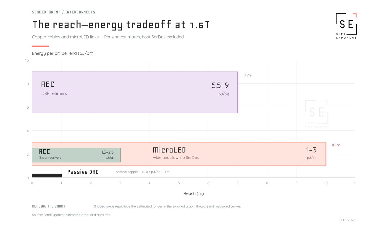
The reach of an active electrical cable (max 10m), at the power consumption of a DSP-less active copper cable (1-3 pJ/bit).
It is clear how microLED occupies an important and attractive tier in the close-reach interconnect space. Especially as the scale-up domain is going multi-rack in the Rubin Ultra and beyond, MicroLEDs provide a solution to connect GPUs both in-rack and across-racks, at an energy-efficiency that is attractive as world-sizes go up.
The setup below shows Avicena’s LightBundle™ which they sample to potential customers along with their software platform shown on their screens. The boxes have transmit and receive circuits, and are used to test the microLED link between them. They have internal waveform generators if you want to use data patterns out of the box, or the front panel has connectors through which customers can provide their own waveforms for testing the optical link.
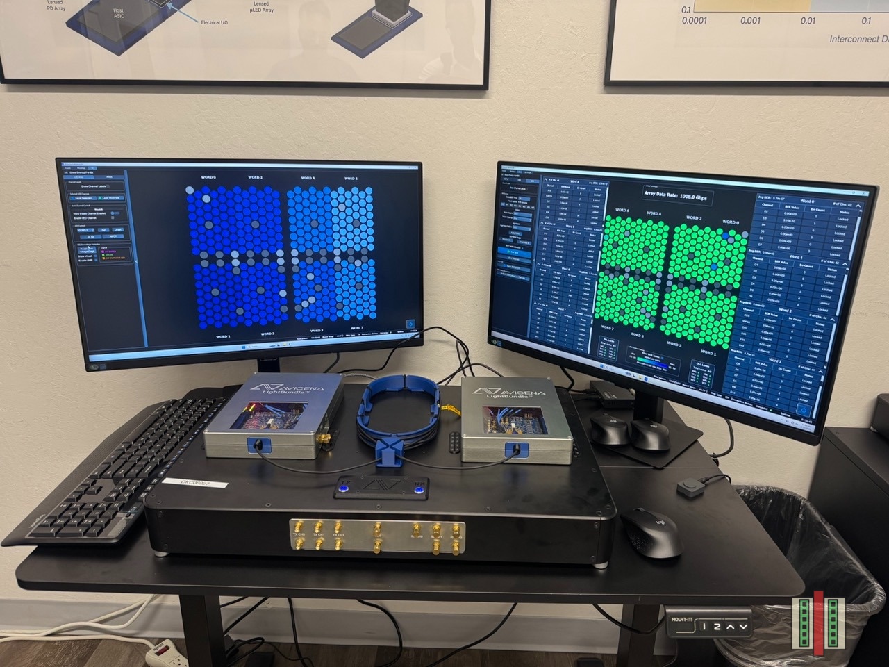
The length of the cable in the middle is approximately 5m in this test, and the diameter of the cable having 300+ parallel links is 3mm. The idea that a bundle of fibers makes the actual cable unwieldy is untrue.
The screens show transmitter data on the left, and receiver data on the right. Each of those hexagons on the screen represent a microLED lane carrying ~3 Gbps of data. You notice there are some blue dots on the grid – those are the points where the link is performing poorly, where the BER is higher than some threshold. The bottom of the screen shows a color scale from green to blue: green = good BER, blue = bad BER. We will see some measurements with this setup next.
第二部分:中文深度解读
一、一句话定位
这不是论文,也不是新闻稿,而是一次实地探访(field trip)后的第一手观察报告——作者在 Hot Chips 之后去 Avicena 待了几个小时,进实验室看 MicroLED 光互连,然后把自己进去之前列好的「质疑清单」逐条对着实物过一遍。
它的价值不在于给出新技术结论,而在于修正了一个常见的认知错位:MicroLED 互连不是「性能更差的光模块」,而是「能跑更远的铜缆」。作者的原话是:“The real competition is copper, not optics.”
同时要清楚本文的边界:免费段只覆盖对象清单、单通道速率(Lane Rates)、传输距离(Reach) 三节;而串扰与抖动、Gearbox、物理构造与制造、结论四节在付费墙后——按常识,后四节才是决定商业成败的部分。
二、作者的立场与利益关系(先读这个,再读结论)
| 项 | 内容 | 对读者意味着什么 |
|---|---|---|
| 赞助 | 明确声明无赞助,唯一「报酬」是现场喝的气泡水 | 无商业稿酬关系 |
| 厂商参与 | Avicena 审阅了本文草稿以核对事实,作者保留编辑独立权 | 文中涉及 Avicena 的事实性描述(波长、速率、通道数、器件结构)基本经厂商确认;但判断性内容(行业走向、对竞品的评价、对 30m 宣传的批评)仍属作者 |
| 现场证据 | 8 张照片,含仪器读数、示波器屏幕、误码仪屏幕、实测台架 | 这是本文最硬的部分,可独立交叉核对 |
| 图表来源 | 两张量化图(速率演进、距离-能耗权衡)均标注 SemiExponent,即作者自家公司的估算/数据库 | 不是第三方实测;图中还自注「阴影区为估计范围,而非实测曲线」 |
| 定位 | 作者同时公开批评厂商对 30m 距离的过度宣传 | 不是「软文」,但属同一信息生态内的行业分析,需分层采信 |
三、对象清单:作者自己立的靶子
作者的框架是「先穷举反对意见,再去现场逐条验证」。他列的六条:
- 单通道速率:MicroLED 太慢,且提速困难;
- 距离:线宽差 → 色散 → 距离受限,10 m 可信,30 m 在好 BER 下是勉强的;
- 光纤数量与对准:速率上不去就得堆通道数,光纤多了线缆笨重、几百根光纤对准 microLED 阵列在量产规模上很难;
- 抖动:MicroLED 噪声大,抖动大,劣化 BER;
- 串扰:几百根光纤捆在一起串扰大;
- Gearbox:IC 侧 SerDes 出的是 8×200G 这类高速通道,要变成 400×4G 需要齿轮箱芯片,很难做。
这里有一个值得单独拎出来的澄清:作者指出「没有多少批评者说清楚他们说的串扰是哪一种」——实际上是两种,①光纤之间的光域串扰,②线缆两端馈入几百条通道的电域通道间串扰。很多讨论把两者混为一谈。
但要注意作者自己的处理方式:他把串扰与抖动的实测结果(受害者/攻击者浴盆曲线、PRBS 同异码型对比)放进了付费段。也就是说,这个最有价值的澄清在免费段只提出了问题,没给答案。
四、Lane Rates:量产 3–3.5 Gbps,8 Gbps 仍是实验室
作者看到的事实
- 器件是 GaN 基,发蓝光,波长 420–440 nm;
- 当前量产工艺 3–3.5 Gbps 每通道;
- 下一代 8 Gbps 器件仍在实验室,且测的是自由空间的极短链路——作者特别强调这一点:把 microLED 几乎贴着探测器照过去,去掉光纤的影响,测出来的只是 microLED 本身的速率能力,不含光纤损耗与色散。
现场三张照片就是这条链路的证据:
- Anritsu MP1763B 脉冲码型发生器,频率 8.000 GHz;
- 示波器眼图:NRZ、收发短链路、自由空间,屏幕日期 2026-08-20,眼图张开、抖动低;
- 误码仪读数 0.0000E-11(优于 1e-11)。
另外,图中那个 10 Gbps 数据点来自 IEEE Photonics Technology Letters 论文(doi 10.1109/LPT.2025.3552708)的 Fig. 7:用外部驱动电路 + 限幅放大器,单通道 10 Gbps、BER 1E-10。作者原文写清楚了限定条件(”external driver circuit instead of an integrated one”),这个限定很容易在转述中丢掉——它不是产品能力,是「用外部仪器把器件推到极限」的演示。
我的独立核对
- 与厂商公开口径一致:Avicena 2026-08 宣布出货 1 Tbps LightBundle 评估套件,335 个 microLED 通道、单通道 3 Gbps;2026-03 OFC 首版是 320 通道(256 活跃 + 64 冗余)、单通道最高 3.5 Gbps、合计 896 Gbps。文中「量产 3–3.5 Gbps」站得住。
- 但有一个口径需要点明:厂商口径的 1 Tbps = 335 × 3 Gbps 的原始(raw)通道速率之和,而不是任何一条链路实际跑通的吞吐。厂商自己公开演示的链路是 512 Gbps(无 FEC 下 BER 优于 1e-10,光纤长度 5 m 或 10 m 可选)。本文免费段出现”1 Tbps”时没有交代这个差别,是最容易被误读的一处。
- “8 Gbps”与”10 Gbps”不能混用:前者是集成 ASIC 驱动的下一代器件,后者是外部驱动器+限幅放大器的论文演示。把 10 Gbps 当作路线图节点会高估进展。
- 作者的结论我认同:单通道速率没有追平 microVCSEL(后者轻松跑 50 Gbps)的路线,出路是「同面积堆更多通道」。
五、Reach:约 10 米是色散给的上限,而对手其实是铜
物理链条
microLED 线宽远宽于激光器(姊妹篇《MicroLED 与激光器之争》给出的量级是 约 40 nm vs 0.001 nm)→ 宽线宽在光纤中经色散导致脉冲展宽 → 码元重叠 → 距离受限。链条本身没有争议,本文的贡献是把它换算成「能不能用」。
两个关键判断
判断一:拿 microLED 去和 >10 m 的 scale-out 光模块比是错的。 作者用词很重:厂商宣传 30–50 m 距离,「把这件事引向了与激光光学的对比,这是错误的思考方式」,并且「希望公司停止对尚未在展会展台上演示过的技术做过度承诺」。他划定的真实战场是 ≤10 m。
判断二:真正的竞争者是铜,不是光。
图 IMG_7 给出的 1.6T 距离-能耗权衡(SemiExponent 估算,主机侧 SerDes 已排除在外):
| 方案 | 能耗 | 距离 |
|---|---|---|
| 无源铜缆(Passive DAC) | 0–0.3 pJ/bit | 1 m |
| 有源铜缆 + 线性 redriver(ACC) | 1.3–2.5 pJ/bit | 约 3 m |
| 有源铜缆 + DSP retimer(AEC) | 5.5–9 pJ/bit | 7 m |
| MicroLED(宽而慢、无 SerDes) | 1–3 pJ/bit | 10 m |
作者的读法是:microLED 在接近线性有源铜缆的能耗水平上,提供了三倍于它的距离,且不需要 DSP。随着 scale-up 域走向多机柜(Rubin Ultra 及以后),microLED 在 10 m 以内提供了一个有吸引力的能效档位。
现场证据
LightBundle 评估套件实拍:两台收发盒子 + 中间约 5 m 的光纤束 + 两台监控屏幕。
- 该线缆承载 300+ 条并行链路,直径 3 mm;
- 左屏发端、右屏收端,屏幕上每个六边形 = 一个 microLED 通道,约 3 Gbps;
- 蓝点 = 该通道 BER 超过阈值的坏点;屏幕底部绿→蓝色标(绿=好 BER,蓝=差 BER)。
作者由此反驳「光纤一多线缆就笨重」的说法。
我的独立核对(这一段最能定性)
① 色散数量级自洽性检查。 用姊妹篇的公式 $\Delta T = D \cdot L \cdot \Delta\lambda$:取蓝光在石英中的色散 $D \approx 500\ \mathrm{ps/(nm\cdot km)}$、microLED 线宽 $\Delta\lambda \approx 20\ \mathrm{nm}$,
| 距离 L | 展宽 ΔT | 3 Gbps(UI = 333 ps)下的占比 |
|---|---|---|
| 10 m | ≈ 100 ps | ≈ 0.3 UI,勉强可用 |
| 30 m | ≈ 300 ps | ≈ 0.9 UI,基本不可用 |
→ 作者的「约 10 m 上限」在数量级上是自洽的,也正好解释了他为什么反对 30 m 的宣传。(注意这是量级核对,不是精确计算:$D$ 与 $\Delta\lambda$ 的取值会显著改变结果,最终应以厂商实测数据为准。)
② 铜侧的横向核对。 按业界公开口径(Marvell 的 AEC 曲线、SemiAnalysis、以及作者自己此前的 OCP APAC 报告):200G/lane 时无源铜 1–2 m、延长型 AEC 约 3 m;100G/lane 时 AEC 可到约 5 m;到 400G/lane,「铜墙」成真。
→ 这精确支撑了作者的判断:3 m(200G AEC 的极限)到 10 m 之间,确实存在一个当前没有好方案的带宽/能耗空档。microLED 的产业位置就在这个空档里。
③ 「300+ 芯 / 3 mm」的物理合理性。 335 根 125 µm 包层光纤六方密排,理论束径约 2.4–2.6 mm,加上护套与加强件到 3 mm 完全合理。→ 「光纤多了线缆就笨重」的质疑在这个通道量级下确实不成立,作者的现场反驳是有依据的。
六、外部补强:这家公司站在什么位置(可独立核对的时间线)
| 时间 | 事件 |
|---|---|
| 2019 | Avicena 成立,总部加州 Sunnyvale |
| 2022-01 | 收购 Nanosys 的 GaN microLED 晶圆厂与工程团队(该厂此前由 glo 投资逾 2 亿美元) |
| 2023-10 | 在 16nm FinFET CMOS 上做出 1 Tbps microLED 收发 IC(ECOC) |
| 2023-11 | SC23 展示其称为「世界最小 1 Tbps 光收发器」 |
| 2024-03 | OFC 宣布 sub-pJ/bit、10 m 的 chiplet 互连平台 |
| 2024-09 | ECOC 展示 30 m 链路——这正是作者批评「过度承诺」的原始出处 |
| 2025-04 | 与台积电合作优化用于 LightBundle 的硅光电探测器阵列 |
| 2025-05 | 完成 Tiger Global 领投的 6500 万美元 B 轮,累计 1.2 亿美元(SK hynix、美光、三星、Lam Research 等参投) |
| 2025-09 | Marco Chisari(前三星晶圆代工美国 EVP)出任 CEO——即文中出面接待的那位 |
| 2025-11 | SC25 宣布 4 Gbps/通道、发射端 80 fJ/bit |
| 2026-03 | OFC 首发 LightBundle eKit(320 通道 / 896 Gbps / 512 Gbps 链路演示) |
| 2026-08 | 出货 1 Tbps eKit(335 × 3 Gbps) |
| 2026-09 | ECOC 展示连接器式 microLED 光互连(MPO 外形 + 为多芯光纤束优化的插芯,支持插拔与现场维护) |
这张时间线本身就是一条重要观察:
- 可达距离的公开记录是 10 m(2024-03)→ 30 m(2024-09)→ 回到 10 m 定位(本文 2026-09);
- 而单通道速率从 2023 年的 4 Gbps 到 2026 年量产的 3–3.5 Gbps,几乎原地踏步。
→ 作者「没有追平 microVCSEL 的路线」这个判断,从公司自己的公开记录看是成立的。这也解释了 Avicena 近两年的重心为什么明显地转向了可部署性与可维护性(评估套件、连接器化、MPO 外形)而不是速率——这恰恰是本文付费段「物理构造与制造」要讲的内容。
另一处值得注意:B 轮投资者里有 SK hynix、美光、三星——是存储厂商而非网络厂商。这与作者的叙事吻合:microLED 的早期买家,可能是要把「内存域」连起来的那批人(XPU↔内存、内存解耦)。
七、可采信度分层
| 内容 | 采信度 | 理由 |
|---|---|---|
| 现场仪器照片与读数(8 GHz PPG、眼图、1e-11 BER) | 强 | 第一手照片,且已由厂商核对事实 |
| 量产 3–3.5 Gbps、335 通道 / 1 Tbps eKit | 强 | 与厂商 2026-08 出货公告一致 |
| 300+ 链路、5 m、线径 3 mm | 强 | 现场实测照片,物理量级合理 |
| 8 Gbps 下一代器件 | 中 | 实验室自由空间短链路,非光纤、非产品;作者已注明条件 |
| 10 Gbps(IEEE PTL) | 中 | 有同行评议论文,但用外部驱动器 + 限幅放大器,不可外推为产品能力 |
| 「约 10 m 是色散上限」 | 中强 | 机制正确、量级自洽;但具体数字依赖 $D$、$\Delta\lambda$ 取值,免费段未给实测 |
| 两张量化图(速率演进 / 距离-能耗) | 中 | 来源为作者自家 SemiExponent 的估算与数据库,非第三方实测 |
| 「microLED 的对手是铜不是光」 | 中强(判断) | 与业界铜缆 reach 数据一致,属有依据的行业判断 |
| 「厂商 30–50 m 宣传是过度承诺」 | 中(判断) | 与 Avicena ECOC 2024 的 30 m 演示对得上;但免费段未给作者自己的反证数据 |
| 串扰/抖动、Gearbox、制造、结论 | 未含(付费墙后) | — |
八、付费墙缺口:为什么这个缺口是结构性的
缺失四节:串扰与抖动(受害者/攻击者浴盆曲线实测)、Gearbox(64:1 vs 4:1 的代价、时钟转发、去斜)、物理构造与制造(收发芯片、300 mm 晶圆上焊球集成 microLED、模压透镜阵列、光纤束对准与连接器、自建 Aixtron 反应腔、量产路径)、结论(30 m 问题、冗余与温度行为、客户 scale-in 需求、1.6 Tbps 下 microLED 的定位)。
为什么这四节的缺失不只是「少读一点」:
- 免费段论证的是「能不能用」,付费段论证的是「能不能大规模做出来」。 而决定商业成败的是后者。
- Gearbox 是「宽而慢」架构最大的隐藏税,而它的绝对值恰好在墙后。 3 Gbps/通道意味着相对 200G SerDes lane 约 64:1 的齿轮比(335 × 3 Gbps ≈ 1 Tbps)。这个数量级的串并转换要付出时钟转发与去斜的代价——免费段承认「gearbox 很难做」,却把成本放在了墙后,读者无法判断这笔税有多重。
- 可制造性这个最硬的证据被拿掉了。 用焊球把 microLED 集成到 300 mm 晶圆,再在 300+ 通道上做光纤束对准——对准公差与良率是这类方案历史上最常见的死因。作者本人在别的文章里就用「混合键合良率导致不切实际的乐观」批评过 CPO,现在轮到他自己把这部分放在墙后。
- 作者反对 30 m 宣传,但没在免费段给出他自己的实测反证。 结论节里的「30 m 问题」才是正面回答。
- 一个关键的单位口径问题也没有在免费段交代:图 IMG_7 的能耗 1–3 pJ/bit 明确标注 host SerDes excluded(主机侧 SerDes 不算在内)。而 64:1 齿轮箱的开销恰恰更可能落在 SerDes/驱动这一侧。拿「1–3 pJ/bit」与「AEC 5.5–9 pJ/bit」直接对比,口径并不对等。
→ 所以结论是:本文(免费段)不足以支撑对 microLED 商业前景的最终判断。它完成的是「这个技术不是我原先以为的那样」这一认知修正,而不是「它必然会赢」的论证。
九、这篇文章(免费段)没有回答什么
- 能耗口径:1–3 pJ/bit 是 per-end 还是总额?含不含 gearbox 与驱动器?图注已排除 host SerDes,但没有把排除项的量级补回来。
- 成本:全文没有任何单链路成本或单位带宽成本的数字。”low cost”是主张,不是数据。
- 可靠性与老化:microLED 寿命、蓝光对光纤与胶材的长期辐照影响,免费段完全未触及(放在付费的结论节)。
- 良率与可制造性:全在墙后。
- 与 NPO/CPO 的正面比较:作者说对手是铜,但 Rubin Ultra NVL576 的跨机柜方案走的是 NPO/CPO。microLED 与 NPO 在同一段距离带上是否重叠、各自在什么条件下胜出——本文没有回答(作者把「1.6 Tbps 下 microLED 与铜的定位」也放在了墙后)。
- 客户侧进度:作者提到「客户的 scale-in 请求」在付费段,免费段没有任何客户名称或部署时间表。
- 一个容易被转述放大的口径问题:335 × 3 Gbps = 1.005 Tbps 是原始通道速率之和,而厂商公开演示的单条链路是 512 Gbps。把”1 Tbps”当成「能跑 1 Tbps 的链路」会高估。
十、与本站其他文章的连接
- 《MicroLED 与激光器之争:线宽如何锁死数据中心光互连的速率上限》——本文的直接姊妹篇。那一篇用第一性原理推出「线宽 → 色散 → 速率上限」,本文则把它落到现场:「10 m 以内、单通道几个 Gbps」是这条物理链条的自然结果。
- 《共封装光学(CPO)224Gbps+ 全栈图景》——那篇的核心结论是「瓶颈清单里几乎没有’光’,封装、良率、驱动电路才是」。microLED 把同一道题换了个形式重考:光域更简单(无激光、无调制器、无 WDM),但把复杂度推给了 gearbox 与 300+ 通道的制造。
- 《华为 OIF NPO 标准化:7.2T 模块》/《NPO 光电链路实验室》——跨机柜 scale-up 的既有答案。microLED 需要回答的是「我与 NPO 的分界线在哪」。
- 《中国 AI 超节点的供应链》——铜缆约 3 m 撞墙、正交背板、NPO 三条路线各赌一个约束。本文的「3–10 m 空档」与那篇的「铜缆撞墙」是同一件事的两个视角。
- 《HBM5 互连信号完整性》——XPU↔内存恰是 microLED 宣称的目标场景之一,可与该文的内存侧带宽/信号完整性约束对读。
十一、一句话结论
免费段完成的是一次认知校准:MicroLED 互连不是「更差的光」,而是「能跑更远的铜」——它在 3–10 m 这个「有源铜缆已到极限、NPO/CPO 又过剩」的区间里,用「宽而慢」的架构换取无激光、无 DSP、1–3 pJ/bit。
单通道速率追不上 VCSEL 已成定局,胜负手因此转移到 gearbox 的成本与 300+ 通道的制造良率上——而这两节恰好都在付费墙后面。所以这份证据能支持的是「值得认真对待」,还不足以支持「必然成功」。作者本人最诚实的一句话,是他反对厂商宣传 30 m 的那一段:一个技术如果真能跑 30 m,是不需要在展台上反复强调的。