The AI Bottleneck Is Moving to Advanced Packaging, Three Japanese Companies Hold the Keys — AI 瓶颈正移向先进封装,三家日本公司掌握钥匙
整理 Asia Next (X-RAY
本文整理自 Asia Next(asianext.substack.com,Substack 专栏),原文发布于 Aug 04, 2026(标题原文:The AI Bottleneck Is Moving to Advanced Packaging, Three Japanese Companies Hold the Keys.,编号 X-RAY #3)。 结构为 正文(英文原文)+ 解析(中文深度解读),方便中英对照阅读。 来源说明:内容经公开页面获取;本发布保留完整英文原文(免费框架全本)并附中文深度解读,仅作信息整理与学习用途,著作权归原作者所有,建议在原站支持作者订阅。 ⚠️ 付费墙提示:原文的付费部分为公司具体标的(Company 1 Nitto Boseki 的 lock 细节、Company 2、Company 3、第四支投机性标的及作者遗漏说明)位于付费墙之后,本发布仅含免费可读框架全本,未转载任何付费内容。文末已标注截断位置。
第一部分:正文(Original Article)
The AI Bottleneck Is Moving to Advanced Packaging, Three Japanese Companies Hold the Keys.
X-RAY #3
Prologue
If you are new here, welcome to Asia Next. We uncover Asia’s most overlooked investment opportunities: hidden world leaders quietly controlling a vital bottleneck of the global tech supply chain, companies whose world-first technologies no competitor can replicate, and strategic players no headline ever mentions. Undervalued today, indispensable tomorrow: that’s where the real upside hides.
Today, we talk about advanced packaging.
Not the chip. The thing that holds the chip together.
A few Days Ago, Nvidia Paid $1.5 Billion In Advance For Glue
Let me start with what happened last Thursday.
On July 23, 2026, Amkor Technology announced a multi year strategic partnership with Nvidia. Under the agreement, Nvidia provides a $1.5 billion prepayment to expand Amkor’s advanced packaging and test capacity in the United States, principally in Arizona. The two companies will align long term roadmaps on high density interconnects and next generation heterogeneous integration.
Amkor shares jumped 17% in extended trading. The stock is up 63% year to date.
Now read that first sentence again, slowly.
Nvidia did not sign a supply contract. Nvidia did not place an order. Nvidia handed a supplier one and a half billion dollars in cash, up front, before receiving anything at all.
Companies do not prepay for commodities. You do not wire money in advance for something you can buy from four vendors next quarter. You prepay when the thing you need is scarce, when the queue is long, and when losing your place in that queue would cost you far more than the prepayment.
The most valuable company in the history of capitalism just paid cash in advance to secure the ability to glue its own chips to memory.
This is not a partnership announcement. It is a hostage payment.
And here is the thing that turned a news item into nine days of research for me. I went looking for context, expecting to find that this was a one off, an aggressive move by an aggressive company.
It is not a one off.
Over the last fourteen months, four other major actors have each done their own version of this. One of them signed a decade long commitment. One of them committed the largest foreign direct investment in American history. One of them spent ten billion dollars building an alternative supply chain rather than keep depending on the one that exists. And one of them quietly deleted a million units from its own product plan, not because demand fell, but because it could not get a slot.
I will show you each of those in turn, at the point in the argument where it actually proves something, because dumping them all in an intro turns evidence into noise.
For now, hold one idea.
The most sophisticated buyers on Earth are not competing for chips.
They are competing for assembly.
And nobody can explain what any of it means
Which brings me to why I actually wrote this edition, and I want to be honest about the motivation because I think a lot of you feel the same way.
For the last eighteen months, every AI supply chain conversation has been drowning about advanced packaging and mysterious acronyms.
But what is even advanced packaging ?
Let me confess something mildly embarrassing.
When I started this research, some stubborn corner of my brain still pictured “packaging” as, you know, packaging. A chip. A little anti static bag. Some bubble wrap. A label with a barcode on it. Off to the post office, next day delivery, sign here please, mind the fragile sticker.
If you pictured anything remotely similar, congratulations, we were both spectacularly wrong.
There is no box. There is no parcel. Nobody is wrapping anything. No van is involved at any point.
The real definition :
Advanced packaging is what physically connects the GPU to its memory (HBM) . An AI accelerator isn’t one chip, it’s a compute die surrounded by stacks of high-bandwidth memory, and advanced packaging is the layer that wires them together into a single component. They have to be connected because the GPU can’t work from memory alone: every token it generates requires reading the model’s weights, so the chip spends most of its time waiting for data rather than calculating. Feeding it fast enough takes thousands of connections running in parallel, packed millimetres apart, far finer than a normal circuit board can route. Without that layer, the GPU and the memory are two separate parts that can’t talk to each other quickly enough, and the accelerator simply doesn’t work.
What actually happens is this. A machine picks up a piece of silicon thinner than a sheet of paper. It aligns that piece to another piece within two microns, which is roughly one thirty fifth of the width of a human hair. It presses them together with precisely controlled force while heating only the joint and not the surroundings, because heating the surroundings would ruin everything. Then it does that two dozen more times, on a structure the size of a dinner plate, which is actively bending while the work happens because its different materials expand at different rates.
Then the whole thing has to stay flat. Permanently. While dissipating enough heat to boil a kettle.
And one stray dust particle in the wrong place destroys a five figure assembly.
It is not shipping. It is surgery.
Honestly, “packaging” might be the single worst piece of branding in industrial history. The word tells you nothing, sounds like cardboard, and has probably cost more investors more money through sheer under-curiosity than any technical term in the sector. If this step had been christened “die integration” or “silicon assembly” back in the 1970s, I suspect half of you would already own these stocks.
Different packaging technologies exist : CoWoS. CoWoS-S. CoWoS-R. CoWoS-L. CoPoS. CoWoP. SoIC. SoW. SoW-X. EMIB. EMIB-M. EMIB-T. Foveros. Foveros Direct. FOPLP. FOCoS. FO-EB. S-Connect.
I count more than twenty five acronyms in regular circulation, most of which sound like the others, several of which are the same thing under different marketing names, and at least two of which are routinely confused with each other by people who write about this for a living.
And here is what I noticed when I started asking around. Nobody understands it. Genuinely nobody. Not retail investors, obviously. But also not most professional analysts, who nod along in earnings calls and then write “advanced packaging remains constrained” as if that sentence contains information.
I watched a well followed finance account confidently explain that CoPoS is the successor to CoWoS. It is not. I watched another confuse glass core substrates with glass interposers, which are two different products several years apart in maturity. I read a broker note that treated EMIB and CoWoS as competing on performance. They are not competing on performance at all.
So the situation, as of this month, is this. The single most important physical constraint on the entire AI buildout is buried under a mountain of jargon that almost nobody has bothered to decode, while the biggest companies in the world quietly wire billions of dollars in advance to secure access to it.
That is a mispricing engine. That is literally how mispricings are manufactured: make something critical, and make it incomprehensible.
So I decided I had to do something about it.
Nine days, one burned pan of rice
I spent the last nine days on this. I read Yole Group’s July 2026 packaging report. I read TSMC’s North America Technology Symposium roadmap. I read Intel Foundry’s material. I read a Mizuho Securities Asia supply chain note that I originally opened for a completely different reason, and which contains the single detail that started this whole investigation, which I will get to.
I built a spreadsheet with forty tickers and deleted thirty seven of them.
I also, on Sunday evening, burned a pan of rice because I was reading about coefficient of thermal expansion mismatch and forgot I was cooking. My partner was not impressed. Worth it.
Here is the stat that ended the research and started the writing.
CoWoS packaging lead times currently extend 52 to 78 weeks.
Fifty two to seventy eight weeks. One year to a year and a half. To **package** a chip that has already been manufactured.
Think about what that means. You can have the silicon. You can have the memory, the design, the software stack, the data centre, the power contract, the customers queued around the block. And you still cannot ship, because there is an eighteen month queue for the step that assembles it
That is not a supply chain that is slowing down.
That is a supply chain with a hard physical ceiling.
By the end of this edition, you will understand every one of those acronyms, you will know exactly where that ceiling sits, and you will know the names of three Asian companies that almost nobody covers and that the entire industry quietly depends on.
Let’s go.
What This Edition Covers
- Why Nvidia prepaid $1.5 billion in cash for packaging capacity, and why four other giants did versions of the same thing this year
- Every acronym in this industry, decoded in plain English, so you never have to nod along again
- The $265 billion embarrassment: America made the largest foreign direct investment in its history, and every AI chip made in Arizona still flies to Taiwan to be finished
- The packaging war splitting the industry into two armed camps, and why it is not a fight about performance atall
AND most of all:
- A full demonstration of what the real bottleneck in advanced packaging is
- The six simultaneous locks on packaging capacity and the recursive trap that means money cannot open them
- The three overlooked Japanese companies that own three of those locks, each holding above 90% share or global technology leadership in something nobody has heard of
- The real risks and friction and my honest opinion
1. The Blind Spot
What everybody is watching
Let’s start with the consensus, because the consensus is not stupid. It is just incomplete.
Right now the market watches three things. Nvidia’s revenue. Hyperscaler capex guidance from Microsoft, Google, Amazon and Meta. And TSMC’s leading edge node ramp: 3nm, 2nm, A16, A14.
That is a rational place to look. These are the visible surfaces of the AI buildout. And the underlying mental model is Moore’s Law: smaller transistors, more compute, better AI.
For fifty years that model was correct.
It is now wrong.
The reversal
Here is what actually happened over the last thirty six months, and almost nobody has updated their model for it.
Transistor scaling has slowed to a crawl. TSMC’s A14 node will deliver roughly 20% higher transistor density than N2 in 2028. Its optical shrink successor, A13, will add about 6% a year later.
Six percent. That is a rounding error wearing the costume of a generation.
Meanwhile AI compute demand is not growing at 6% per year. It is growing at a rate that makes 6% look like a typing error.
So where does performance come from now?
It comes from putting more silicon into one package. Not smaller silicon. More of it, stitched together.
This is the part the market has not internalised. The industry stopped scaling **down** and started scaling **out. And when you scale out, the limiting factor is no longer the lithography tool. It is the **assembly step: the interposer, the substrate, the bonder, the material underneath.
TSMC said it out loud in its own roadmap material: “AI compute scaling is driven by the combination of advanced logic, SoIC 3D stacking, and CoWoS technologies.”
Read that again. Logic is listed first, but it is one item of three. Two of the three are packaging.
It is not a chip problem anymore. It is an assembly problem.
The bottleneck, in one sentence
Here it is, without naming a single company:
Every frontier AI accelerator on Earth must pass through an advanced packaging line. There are only a handful of such lines in the world. All of them are booked out for more than a year. And all of them depend on a tiny number of machines and one near monopoly material.
That is the whole thesis.
The bottleneck is shifting.
It’s no longer just “can we design faster chips?”
It’s “can we package and ship thm fast enough?”
This is how bottlenecks quietly move through the system.
First design.
Then fabrication.
Now packaging.
Why nobody thinks about it
Five reasons, and they are all structural, which is exactly why the mispricing persists.
One: it is the back end. For forty years, packaging was where chips went after the interesting part was finished. It was called “assembly and test.” It was low margin, outsourced, moved to Malaysia and the Philippines because it was labour work. Careers were not made in packaging. Analysts did not cover packaging. The word itself sounds like cardboard boxes.
Two: it is invisible B2B. You cannot buy an interposer. There is no consumer product. These companies sell to five customers, sign NDAs, and never appear in a keynote.
Three: it is deliberately incomprehensible. Twenty five acronyms, several of them describing the same thing under rival marketing names. Complexity is a moat, and it is also a fog. Value hides in fog.
Four: it is filed under the wrong headings. The companies I will show you are classified as, variously, a textile manufacturer, an industrial machinery maker, and an electronics assembly company. None screens as AI. When a fund manager runs a semiconductor screen, these names do not appear. This is category misfiling at industrial scale.
Five: the numbers look small until they are not. Total back end equipment is a roughly $6.9 billion market. Next to a multi trillion dollar AI narrative, that reads as noise. But a $6.9 billion market that gates a multi hundred billion dollar market is not small.
It is a toll booth.
What happens if this link fails
Let me make this concrete, because abstractions do not build conviction.
If advanced packaging capacity disappeared tomorrow, here is what happens to the AI industry.
Not “it would be delayed.” Not “margins compress.”
It stops.
Not slows.
Stops.
Every Blackwell GPU requires CoWoS-L. Every Rubin GPU requires CoWoS-L plus SoIC. Every Google TPU, every AWS Trainium, every AMD Instinct, every Broadcom custom ASIC requires a 2.5D package. Without the package, a GPU die is a very expensive rectangle of sand that cannot talk to memory. It has no input or output path. It cannot be soldered to anything. It is inert.
You do not get a slow AI industry. You get no AI industry.
Exhibit A: the million units Google deleted
This is the first of the four data points I promised you in the intro, and it is the one that proves the constraint is already binding rather than theoretical.
In late 2025, Google cut its 2026 TPU production target by one million units.
Sit with that number. Not a slipped launch. Not a delayed quarter. A million accelerators, removed from a production plan, at a company that had already paid to design them.
And the reason was not demand. Google’s problem in 2025 was that it could not build TPUs fast enough to satisfy its own internal consumption, let alone external cloud customers. The reason was not the fab either. The wafers were available.
The reason was that TrendForce reported both CoWoS-L and CoWoS-S, TSMC’s chip assembly platform, fully booked, and Google could not get an allocation.
Google. One of the five most capitalised companies in human history, with effectively unlimited capital, a decade of custom silicon experience and one of the deepest engineering benches on Earth.
It could not get a slot.
That is not a supply chain constraint. That is a sovereignty constraint on compute itself.
And here is what I want you holding for the next twenty pages.
If a constraint is severe enough to make Google delete a million units of its own flagship product, then whoever sits on top of that constraint is not a supplier. They are a toll collector on the entire AI economy.
There are three of them. They are all listed. Two of them hold above 90% global share of something you have never heard of. All three are classified by the market as something they are not.
I will name them at the end, and I will show you exactly why they belong in a portfolio no matter which packaging technology eventually wins.
Hold that, because it explains almost everything that follows. Every architectural decision made by every hyperscaler since late 2025 has been made by people who watched that happen and decided it would not happen to them.
Exhibit B: the $265 billion embarrassment
If you want the single cleanest illustration of how badly the market has misjudged this, here it is.
TSMC has now committed $265 billion to Arizona: twelve fabs, four packaging facilities, the largest foreign direct investment in American history. Its Q2 2026 results were extraordinary. Revenue NT$1.27 trillion, roughly $40.2 billion, up 36%. Net income NT$706.56 billion, roughly $22 billion, up 77.4%. Gross margin 67.7%. High performance computing was 66% of quarterly revenue. Capex guidance raised to $60 to $64 billion.
And yet: every AI accelerator manufactured at TSMC’s Phoenix fab is still flown to Taiwan to be packaged. All of them. And that stays true for at least two more years.
The United States spent a quarter of a trillion dollars and still cannot finish its own AI chips at home.
Guys, that is kind of insane when you say it out loud. You can build the most advanced silicon on the planet in the Arizona desert, and then you have to put it on a plane to Taiwan so that someone can attach it to its memory.
The wafer is the easy part now. The attaching is the hard part.
And look at what TSMC actually did about it, because this is the detail the coverage skipped. Of the twelve planned facilities, four are packaging plants. C.C. Wei framed that component explicitly as serving multi year customer demand. A third of the largest industrial commitment in American history is being spent on the step everybody calls the back end.
Then, in June 2026, TSMC went further and signed a ten year agreement with Amkor for advanced packaging in Arizona.
Ten years. Not three. The largest and most vertically capable foundry on Earth, a company that has spent forty years insisting on doing things itself, locking a decade of outsourced assembly capacity at a third party.
You do not sign a decade unless you believe the scarcity lasts a decade.
Historically this reminds me of Britain and the Suez Canal. Britain built the world’s largest merchant fleet, controlled the ports, dominated the shipping lanes. And then discovered that a hundred mile ditch in Egypt decided whether any of it mattered. Owning the fleet is not the same as owning the chokepoint.
The market owns the fleet.
I want the ditch.
2. How We Got Here
Twenty years, compressed
Until roughly 2012, chips were monolithic. One die, one package. Packaging meant running a wire from the die to a pin. Moore’s Law did all the work and nobody thought about the back end.
2011 to 2012: the first crack. Xilinx shipped an FPGA that stitched four slices together on a passive silicon interposer. TSMC called the technique CoWoS. A niche solution to a niche problem. Almost nobody cared.
2016 to 2017: two things happened at once. HBM, high bandwidth memory, started shipping in volume, which forced memory to sit physically beside logic on a shared interposer. And Intel introduced EMIB, burying a small silicon bridge inside the package substrate instead of using a full interposer. Two rival philosophies were now on the board.
2017 to 2020: chiplets went mainstream. AMD proved you could beat a monolithic competitor by cutting your processor into pieces and reassembling it. This was an economic argument as much as a technical one, because smaller dies yield better, so a chiplet processor is cheaper to build than one giant one. The industry noticed.
2020 to 2022: transistor scaling visibly decelerated. Full node density gains fell to 15% to 20% every three years. The growth engine started coughing.
Late 2022: ChatGPT.
2023 to 2024: the crunch. AI accelerators outgrew the maximum printable chip size. Every hyperscaler simultaneously decided it needed custom silicon. CoWoS demand went from roughly 370,000 wafers in 2024 to about 670,000 in 2025. TSMC’s monthly capacity at end 2024 was around 35,000 wafers. Do the arithmetic. It did not work.
2025 to 2026: the scramble. TSMC quadruples capacity. Intel resurrects EMIB as a commercial weapon. AMD funds a separate Taiwanese packaging ecosystem with ten billion dollars. Nvidia explores a design that deletes the substrate entirely, then prepays Amkor $1.5 billion for capacity. Every OSAT in Taiwan builds panel lines.
And here we are.
Why now: the four things that changed
One, the size wall became binding. I will explain this properly in the next section, but the short version is that there is a hard physical maximum to how large a single chip can be printed. AI accelerators hit it. Once you hit it, packaging is the only way forward. This is physics, not strategy.
Two, the demand curve went vertical. Total CoWoS demand approaches 1.0 million wafers in 2026, up from about 370,000 in 2024. A tripling in two years. TSMC has been expanding capacity at roughly 80% per year: about 35,000 wafers per month at end 2024, about 75,000 at end 2025, targeting 120,000 to 140,000 by end 2026, with Mizuho now modelling 190,000 to 200,000 by 2027.
Here is the part that should stop you.
The lines are still fully booked.
Capacity quadrupled and the queue did not shorten. When supply quadruples and the waiting list does not move, that is not a cyclical shortage. That is structural, sustained, multi year demand that nobody can serve.
The thing almost nobody says out loud
AI demand is software. Supply is physical.
Demand compounds and deploys over a weekend. A model ships on a Friday and by Monday it is consuming compute in forty countries. Supply arrives in steps, and every step has a construction time you cannot pay to shorten.
These are not two curves running at different speeds. They are two curves of different kinds.
A model ships on a Friday. A cleanroom takes three years. A glass furnace ordered today produces in 2028.
That is why capital does not fix this, and it is worth sitting with, because it is counterintuitive in an industry where capital fixes almost everything. Nvidia can wire $1.5 billion in advance and concrete still cures at the speed of concrete. TSMC can spend $64 billion in a year and the drawing equipment for specialty glass still has a multi year queue.
And it gives us the rule that organises this entire edition:
The more physical the layer, the slower it responds, and the longer the bottleneck sits there.
Hold that rule. It is the reason the constraint travels in the order it does: assembly first, because a line can be built in two to three years. Substrates next, because a substrate fab takes longer and there are fewer of them. Materials last, and longest, because a glass composition and the craft of spinning it cannot be built at all. They have to be learned.
Keep that last sentence in mind, because it is the whole reason this edition ends where it ends. The slowest layer is the most valuable one to own, and almost nobody owns it, because almost nobody has bothered to work out where it is.
Three, concentration became a strategic emergency. Nvidia holds roughly 60% of CoWoS capacity. The top three customers have locked more than 85%. If you are customer number four, and here “customer number four” means a company like Google or Amazon, you are structurally starved. This is what forced the packaging war. It was not a technology decision. It was a procurement decision.
Four, geopolitics arrived. Concentration is not only corporate, it is geographic. Yole Group put it precisely in its July 2026 report: TSMC’s CoWoS capacity, Ajinomoto’s ABF substrates and one Japanese producer’s dominance in specialty glass cloth make Japan and Taiwan the critical chokepoints for AI packaging.
The “why now” in one line
Because the industry’s growth mechanism physically relocated, from the front end to the back end, while the market’s attention did not move at all.
This is not a story about a shortage. It is a story about a relocation.
The gap between where the value moved and where the attention stayed is the opportunity. And it has a shelf life. The window is narrowing
The size of the prize
Quickly, before we go into the physics, so you know what is being fought over.
Yole Group’s July 2026 assessment puts the advanced packaging market at $55 billion in 2025, exceeding $120 billion by 2031. More telling than the number is the structural claim attached: advanced packaging is overtaking traditional packaging to become the dominant segment, and should be the majority of all packaging revenue by 2031.
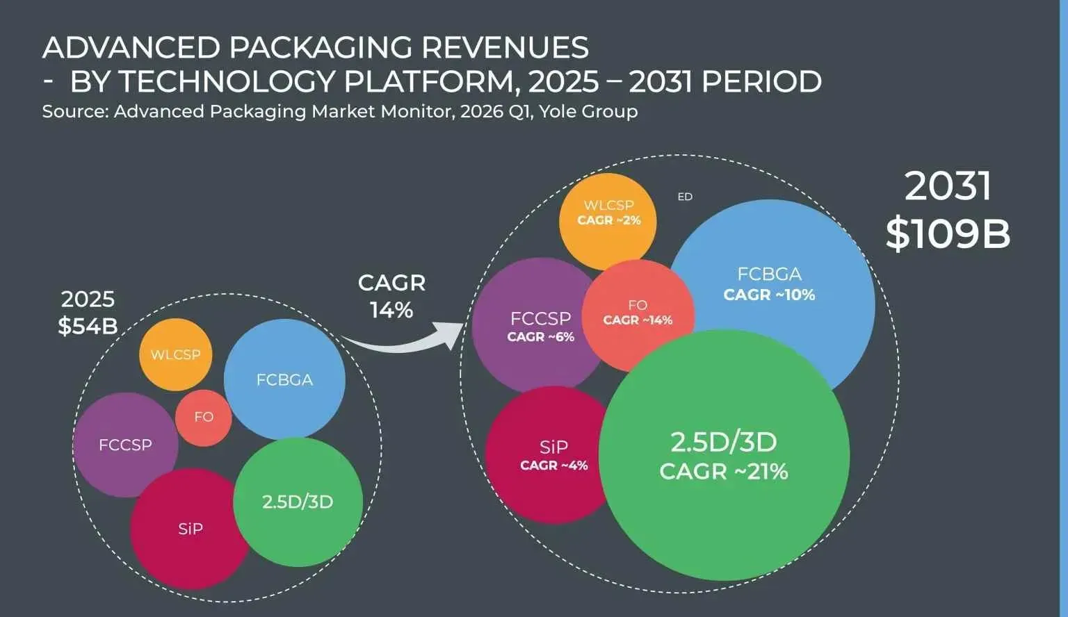
The high value core compounds much faster. High end performance packaging, the chiplet integration segment serving AI, reaches $28.5 billion by 2030 at 23% annual growth. Advanced IC substrates add another $31 billion by 2030.
Yole’s Bilal Hachemi put it in a sentence that deserves pinning above every semiconductor analyst’s desk:
“Advanced packaging is no longer a backend afterthought. It has become the physical layer that decides AI-compute availability, memory bandwidth, power delivery, and system cost. That is a structural shift, not just a growth cycle.”
A structural shift. Not a cycle.
And there is a second demand wave that almost nobody has priced. AI server CPUs. Mizuho expects AI application server CPU demand to grow more than 50% year over year in 2027, with ARM based server CPUs more than doubling: Nvidia’s Vera above 7 million units, AMD’s Venice at 5 million, Google above 4 million, AWS above 3 million.
These need advanced packaging too. The market has modelled the GPU wave. It has not modelled the CPU wave stacked on top of it.
3. The Technology, Decoded
3.1 What a package is, and the wall it hit
The baseline
A chip is a rectangle of silicon a few centimetres across. It cannot connect to anything by itself. The package is the structure that carries it. It takes the thousands of microscopic contacts on the underside of the die and fans them out to contacts big enough to solder onto a circuit board.
The standard method is flip chip on organic substrate. The die is flipped upside down and its bumps are soldered onto a multilayer resin board called the substrate. That substrate is built from ABF, meaning Ajinomoto Build up Film.
Yes, that Ajinomoto. The Japanese company that makes MSG seasoning. A by product of their amino acid chemistry turned out to be the best insulating film in the world for chip substrates, and they have dominated it ever since. Modern AI substrates use fifteen or more routing layers of the stuff.
Pause on that for a second, because it sets the tone for everything that follows. The most advanced computers ever built sit on a film invented by a seasoning company. This industry is full of that. Keep it in mind.
Open up the substrate, because it comes back later
Before we move on, cut one of these substrates in half and look at what it is actually made of. This takes ninety seconds and it is the single most useful thing in this section, because in Part 4 every one of these four items turns out to be a global chokepoint.
A substrate is a laminate. Four physical inputs, each doing a different job:
- Woven glass cloth. The skeleton. Fabric, literally woven on looms, that gives the board its dimensional stability and stops it deforming under heat.
- Resin and build up film. The insulation between layers. This is where ABF lives.
- Copper foil. The conductor. Etched into traces that carry signal and power across every layer.
- Drilled microvias. The vertical connections. Tens of thousands of holes, bored mechanically through the stack to join the layers.
Skeleton, insulation, conductor, hole. That is a substrate.
Now hold two things in your head as you read the rest of Part 3.
First: every packaging architecture I am about to describe still lands on one of these. CoWoS, EMIB, panel packaging, all of it. The interposer, the bridge and the 3D stack are what sit above** the substrate. They do not remove it. Chip on wafer **on substrate is right there in the name.
Second: everything the roadmap does makes the substrate harder. Bigger packages mean more area to keep flat. More chiplets mean more input and output pins, which means more routing layers and more holes. Faster signalling means the copper has to be smoother. Each step on the roadmap is also a step up in what the four materials underneath must survive.
Remember the four. We come back to them.
And I will be blunt about where this is going, because I would rather you read the technical section knowing what it is for. Three of those four inputs are effectively controlled by single companies. Not oligopolies. Single companies, with shares above 90%, that no AI index contains and no semiconductor screen returns
The wall: what a reticle actually is
Now the single most important number in this entire industry, and I want to explain the concept properly because it gets thrown around constantly without definition.
Chips are not drawn. They are printed, photographically. A machine called a scanner shines light through a patterned mask and projects that pattern onto a silicon wafer coated in light sensitive chemicals. Think of a cinema projector, except the image is a circuit and the screen is silicon.
The reticle is that mask. And like any projector, there is a maximum image size the optics can project in a single shot, cleanly and in focus, everywhere.
That maximum is 26 millimetres by 33 millimetres.
858 square millimetres. Slightly smaller than a credit card.
When you read “one reticle” in this industry, that is what it means: one full exposure, the biggest single continuous piece of circuitry the machine can print in one go. When you read “5.5 reticle,” it means an assembled structure with the area of five and a half of those exposures stitched together.
And this limit is not a cost constraint or an engineering preference you can negotiate around. It is the optical geometry of the lithography tool. It is as fixed as the focal length of a lens.
AI accelerators wanted to be bigger than a credit card. So the industry did the only thing available. It stopped trying to print one big chip and started assembling several smaller ones, called chiplets, into a single package that behaves like one enormous chip.
Which gives us the question that defines the entire sector:
How do you make separate pieces of silicon talk to each other fast enough that they pretend to be one chip?
Answer that and you have advanced packaging.
The analogy
Think of a chip as a city and transistors as buildings.
For fifty years, progress meant making buildings smaller so you could fit more inside the city limits. That worked until the buildings got so small that shrinking them further stopped helping.
So the industry built satellite cities, which are chiplets. And now the entire challenge is the transport network between them. Not the buildings. The roads.
Advanced packaging is the road network. And right now every road building crew on Earth is booked out for eighteen months.
The four axes, and the dimensional vocabulary
Every technology in this sector varies along four independent dimensions. Hold these and nothing that follows will confuse you.
And the dimensions:
Almost everything that follows is 2.5D. The war I am about to describe is a civil war inside 2.5D, two ways of doing the same job.
Three more definitions you need:
RDL means Redistribution Layer. Thin metal wiring layers built directly onto the package, finer than a substrate but coarser than silicon.
TSV means Through Silicon Via. A vertical copper tube drilled straight through a piece of silicon to carry signal or power from top to bottom.
Interposer means a slab of silicon with wiring on it and no transistors. It is a circuit board made of silicon, at lithography pitch instead of PCB pitch.
3.2 The incumbent: CoWoS
CoWoS means Chip on Wafer on Substrate. TSMC’s platform. The de facto standard for essentially every AI and HPC processor in production.
The name is the sequence. Chips (GPU or CPU + HBM) go on a wafer, meaning a carrier that holds the interconnect layer, and that assembled module goes on a substrate. Chip, on wafer, on substrate.
Three variants, and the only difference between them is how much silicon is used to do the connecting.
CoWoS-S, full silicon interposer. A large slab of silicon sits under all the chips, carrying fine pitch wiring plus TSVs to route down to the substrate. Maximum density, maximum cost, because you are burning real wafer area on wiring. And crucially the interposer itself must be printed, so it is capped by the same reticle limit, reaching roughly 3.3 reticles with stitching. This packaged the H100 and H200 generation, and Google’s TPUs.
CoWoS-R, RDL only. No silicon interposer at all. Connection is redistribution layers. Cheapest of the three, lowest density. Good where you need many chips together but not maximum bandwidth between them. Broadcom’s networking and ASIC products lean here.
CoWoS-L, local silicon bridges. The current champion, and the reason this generation exists. Instead of one giant silicon slab, you embed small silicon bridges, called LSI for Local Silicon Interconnect, only where two chips need to exchange enormous bandwidth. Everywhere else you use cheap RDL.
It is the difference between paving an entire county in asphalt and building motorways only where the traffic actually is.
This solves three problems at once. You use far less silicon, so cost falls. You are no longer bounded by the reticle size of a single interposer, so packages get bigger. And you put density exactly where the design needs it.
Blackwell uses CoWoS-L. Rubin uses CoWoS-L. AMD’s Instinct line is moving there. When people say “the CoWoS shortage,” they overwhelmingly mean CoWoS-L.
And note what all three variants share, because it matters later. All of them finish on an organic substrate. The S, R and L refer only to how the chips are wired to each other laterally. Underneath that, in every case, sits the same laminate of glass cloth, resin, copper foil and drilled holes. Every CoWoS wafer TSMC produces creates demand for one of the largest, highest layer count substrates in the industry.
CoWoS capacity going from 35,000 to 200,000 wafers per month is therefore also a substrate demand forecast. And a glass cloth forecast. And a copper foil forecast.
Read TSMC’s roadmap that way and it stops being a technology announcement. It becomes an order book for four companies whose names are not in it.
Where it is now, and where it goes
TSMC is in mass production on 5.5 reticle CoWoS with yields above 98%. Five and a half times the maximum printable chip size, at a yield that would have been considered fantasy five years ago.
The published roadmap from the 2026 North America Technology Symposium:
Let me convert that last row into something human, because “14 reticle” means nothing to a normal person.
A 14 reticle interposer measures 12,020 square millimetres. That is roughly the size of a compact disc. Slightly larger, actually. A small dinner plate.
We are going to build a single computer chip the size of a CD, assembled from two dozen separate pieces of silicon, each manufactured to tolerances measured in atoms, all of it bonded flat to within a few microns, which is about one twentieth the width of a human hair, and it has to stay flat while dissipating multiple kilowatts of heat.
TSMC projects that a 2029 package carries 48 times more compute transistors and 34 times more memory bandwidth than a high end 2024 package.
Forty eight times, in five years. Moore’s Law never did that.
But notice where the gain comes from. Only about four times comes from transistor scaling. The overwhelming majority comes from packaging more silicon together.
It is not Moore’s Law anymore. It is Packaging’s Law.
Who actually makes this possible
Here is something you will not find in the TSMC press release, and it is the thread I want you to follow through the rest of this section.
TSMC does not manufacture the tools that place those chiplets. It does not manufacture the glass cloth that reinforces the substrate. It does not manufacture the film that insulates it, or the compound that encapsulates it, or the polishing systems that prepare surfaces for bonding.
Those come from a very short list of suppliers, mostly Japanese, one Singaporean, several of whom have market shares that would trigger antitrust review in any industry the public understood.
Every time you read “TSMC achieved 98% yield,” what actually happened is that a dozen specialised suppliers, most of whom you have never heard of, each solved an extremely narrow physics problem, and TSMC integrated the results.
Hold that thought.
3.3 The challenger: EMIB and EMIB-T
Now the other camp.
The architectural difference
Intel’s EMIB means Embedded Multi die Interconnect Bridge. It solves the identical problem with one structural change.
CoWoS-L puts the silicon bridge above the substrate, inside an RDL layer built at wafer level.
EMIB buries the silicon bridge inside the substrate itself.
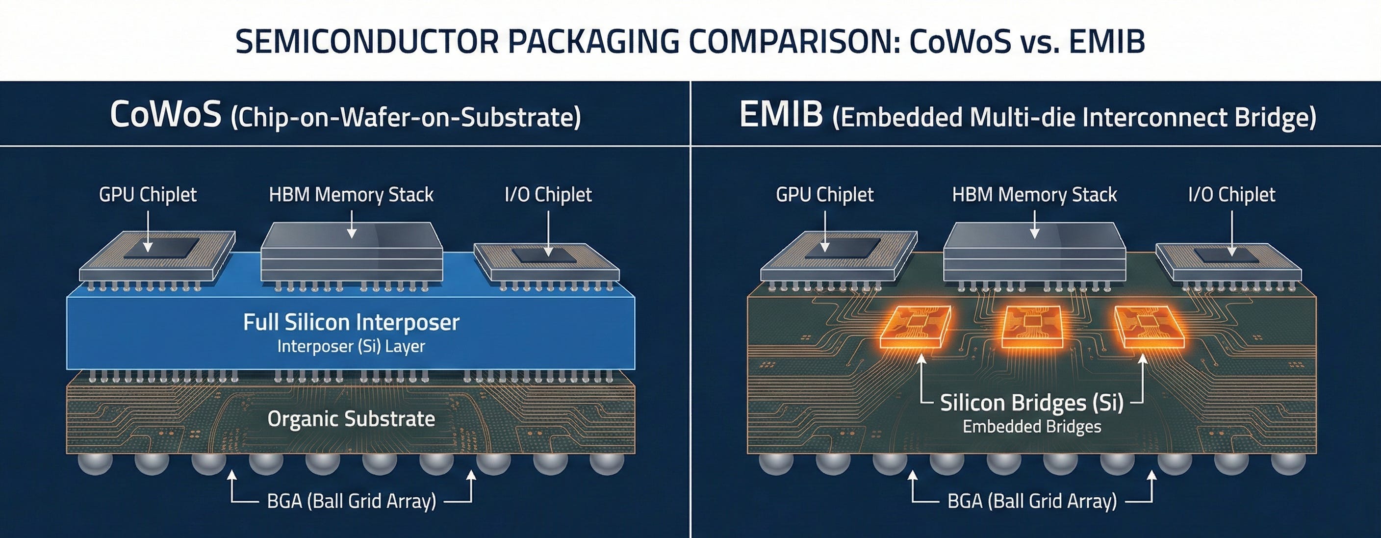
Same concept. Different location. And that one difference cascades through the whole manufacturing flow.
Because the bridge sits inside the substrate, EMIB eliminates the wafer level assembly step that CoWoS requires. No interposer to build, no carrier wafer, no chip on wafer stage. You make a substrate with a bridge in it, and you mount chips on it.
Which has a consequence almost nobody draws out, and it will matter a great deal in Part 4. EMIB does not reduce demand on the substrate. It increases it. CoWoS keeps the hard interconnect work in a separate silicon layer above the laminate. EMIB pushes that work down into the laminate, embedding a silicon component inside a structure made of woven cloth and resin, which must then survive thermal cycling without cracking or delaminating around it.
So the two rival architectures are not rival sources of demand for the materials underneath. One needs an excellent substrate. The other needs a more excellent substrate.
Start noticing this pattern, the packaging war has two possible winners at the architecture level and the same handful of guaranteed winners underneath it. You do not have to pick a side. You have to work out who supplies both sides.
It also means the package has no reticle derived size ceiling, because nothing package sized has to be printed by a scanner.
The family, classified by what is inside the bridge
- EMIB, bare bridge, in mass production since 2017
- EMIB-M, adds MIM capacitors inside the bridge, improving power integrity
- EMIB-T, adds TSVs to the bridge
EMIB-T is the one that matters. A plain EMIB bridge only carries signals sideways. It cannot pass power vertically. On a modest package that is fine. On a multi kilowatt AI accelerator drawing enormous current, it is disqualifying, because you cannot get enough power up to the dies.
Adding TSVs turns the bridge into a vertical power conduit as well as a horizontal data road.
There is a nice technical irony here. The strict definition of 2.5D requires through vias in the interconnect layer, which classic EMIB lacks, so some taxonomists file it as “2.3D.” EMIB-T is the version that makes Intel’s approach fully 2.5D, and it becomes commercially viable at exactly the same moment. The technical fix and the commercial unlock are the same event.
Do not settle it on performance
You will read a lot of noise about whether CoWoS or EMIB is “better.” Ignore all of it.
Intel argues EMIB removes wafer level steps, shortens cycle time, cuts cost and has no reticle based size limit. TSMC argues it delivers the largest package in the industry by reticle size.
Both are true. They measure different things.
The war is not being decided on microns. It is being decided on availability.
Exhibit C: the customers voting with their tape-outs
This is the third data point, and it is where the abstract argument becomes a set of dated, named commitments.
Mizuho reports that EMIB-T interconnect yield has passed 95%, with Intel in active discussions with MediaTek, Ampere Computing, AWS and Tesla.
Then it got concrete:
- MediaTek, at Goldman Sachs Taiwan Day, stated its next generation program adopts only EMIB-T, tape out targeted 4Q26, mass production 4Q27. Not “evaluating.” Not “dual sourcing.” Only.
- Google is reported to be using EMIB-T for its next generation TPU, and has reportedly booked Intel to package more than three million TPUs in 2028.
- SK hynix, a memory company rather than a logic company, is testing Intel’s 2.5D EMIB for memory integration.
- Taiwanese suppliers Powerchip and AP Memory have been pulled into the EMIB-T orbit around Google’s TPU program.
- Intel has begun outsourcing EMIB assembly to Amkor in Korea, with further sites planned in Portugal and Arizona.
Intel Foundry generated just $307 million in external revenue not long ago. CFO David Zinsner has called advanced packaging the “brightest spot” for Intel Foundry, with engagements crossing from hundreds of millions into the billions.
So why is this happening? Did Intel suddenly out engineer TSMC?
No.
Look at the second bullet again and connect it to Exhibit A. The company booking Intel for three million units in 2028 is the same company that deleted a million units from its 2026 plan for lack of a CoWoS slot.
That is not a coincidence. That is cause and effect, printed in a supply chain report.
It is happening because Nvidia holds roughly 60% of CoWoS capacity, the top three hold more than 85%, and everyone else got tired of being customer number four.
It is not a technology win. It is a second source decision.
That is the most important sentence in this section. Every hyperscaler learned the same lesson in late 2025: single sourcing your packaging means a competitor can starve you. Google made the lesson expensive and public, and everybody else took notes.
They are not buying EMIB because it is better.
They are buying it because it is not TSMC.
3.4 The second front: SoIC, Foveros, hybrid bonding
First, where we are on the map
Stop for a moment, because we are about to change axis and it is worth being explicit about it. Otherwise the next set of acronyms will feel like more of the same, and they are not.
Go back to the four axes from section 3.1.
Everything in 3.2 and 3.3 lived on axis one, lateral interconnect. CoWoS-S, CoWoS-R, CoWoS-L, EMIB, EMIB-T. Every one of them is an answer to the same question: how do chips sitting side by side talk to each other? They are genuine competitors, they solve the identical problem, and a designer picks one.
We are now moving to axis two, vertical stacking. Different question entirely: how do chips sitting on top of each other talk to each other?
And this is the single most common misunderstanding in the sector, so let me be blunt about it.
SoIC and Foveros are not competitors to CoWoS. They are not alternatives to EMIB. They are a different axis, and they get added on top.
What gets stacked, and what for
Before any of the acronyms, the two questions you should be asking: which chips actually go on top of each other, and why bother?
What gets stacked. Logic on logic. A compute die on another compute die, or a slab of cache memory directly on top of a processor die. AMD’s 3D V-Cache is the consumer example: a layer of cache sitting on the processor rather than beside it. Inside TSMC’s SoIC, it is compute chiplets stacked on compute chiplets.
And here is the part almost everyone gets backwards, so let me kill it immediately:
Vertical stacking is not how the processor talks to its memory. That link is lateral, and it is exactly what CoWoS and EMIB are for. The memory sits beside the compute stack, not under it.
What it is for. Three things, and the third is the one that decides modern designs.
Density. More silicon per square millimetre of package footprint, at a moment when footprint is the binding constraint.
Bandwidth. Two functions that need to exchange enormous amounts of data no longer sit millimetres apart. They sit microns apart. Connection count goes up by orders of magnitude.
Energy. Moving a bit of data across a package costs power in direct proportion to the distance it travels. Shorten the path and the energy per bit falls. On a machine drawing multiple kilowatts, that is not a refinement, it is the difference between a product and a space heater.
Picture a finished AI package as an office block. The vertical stack is floors of the same building, joined by staircases. The memory is the building next door, reached by a walkway. The substrate is the ground both stand on, with the roads leading out to the rest of the city.
3.5D is simply the moment the industry started building upward instead of only spreading outward.
And note what that does to the layer underneath, because it matters later: a taller building on the same footprint needs more power delivered up through the ground it stands on, and more connections down into it. Every floor you add makes the substrate work harder.
Neither camp is selling a 2.5D product anymore. TSMC’s offer is not CoWoS-L, it is CoWoS-L plus SoIC. Intel’s offer is not EMIB-T, it is EMIB-T plus Foveros Direct. Any comparison of the two that stops at the lateral axis is describing a duel while ignoring both combatants’ main weapon.
Hybrid bonding, explained simply
Conventional 3D stacking connects two stacked chips with microbumps, which are tiny solder balls tens of microns apart.
Hybrid bonding removes the solder entirely. You polish both surfaces to atomic flatness, align them, and press them together so the copper pads fuse directly, copper to copper, while the surrounding oxide bonds at the same time.
No bumps. No solder. Direct metal contact.
The gain is not incremental. Connection density rises by orders of magnitude, electrical resistance collapses, and the vertical distance between two chips becomes almost nothing.
The cost is that it demands cleanliness and flatness at a level that is genuinely hard to describe. Surface variation is measured in nanometres. A single particle ruins the bond. This is why the global tool count is so small, and I will come back to that number because it is central to the investment case.
The two camps, again
TSMC’s SoIC means System on Integrated Chips. Two flavours: SoIC-P uses microbumps, SoIC-X is bumpless hybrid bonding. Bond pitch sits at 6 microns today, with a roadmap to 4.5 microns by 2029.
Six microns. A human hair is roughly 70 microns across. So the connections between stacked chips are spaced about twelve times finer than a hair, and the roadmap takes that to sixteen times finer.
TSMC claims 56 times higher interconnect density and five times better energy efficiency versus its 2015 era CoWoS.
Intel’s Foveros covers the same axis. Foveros-S uses a silicon interposer, Foveros-R uses RDL, Foveros-B uses a bridge. Notice they map exactly onto the lateral interconnect axis from our four axis grid, which is a nice confirmation that the framework holds across both ecosystems. Foveros Direct is Intel’s hybrid bonding implementation.
Intel’s stated ambition: Foveros 3D combined with EMIB-T scaling to 12 times reticle size, with sixteen compute dies in a single package.
The number that reveals the real trend
TSMC plans to expand SoIC capacity at Chiayi from roughly 10,000 wafers per month today to 50,000 by 2027.
Five times, in about eighteen months. TSMC guides CoWoS capacity growth at an 80% compound annual rate from 2022 to 2027, and SoIC at 90%.
The vertical axis is growing faster than the horizontal one. Nvidia is expected to absorb most of that expansion.
So when you model this sector, do not model “2.5D packaging.” Model the stack: lateral interconnect plus vertical stacking, as one product.
3.5 The other belligerents: OSATs and hyperscalers
Two groups decide how this war ends, and neither is TSMC or Intel.
The OSATs, arms dealers to both sides
OSAT means Outsourced Semiconductor Assembly and Test, the independent packaging houses: ASE, SPIL, Amkor, Powertech.
For years they were the low margin end of the industry. Not anymore. And the delicious detail is that the same subcontractor now arms both armies:
- TSMC is outsourcing 240,000 to 270,000 CoWoS wafers per year, primarily to Amkor and SPIL, and signed a ten year Arizona agreement with Amkor in June 2026.
- Intel is outsourcing EMIB assembly to Amkor in Korea.
- And on July 23, 2026, Nvidia prepaid Amkor $1.5 billion.
Amkor builds for all of them. When every side of a war buys rifles from the same factory, the factory has a rather good business model. That is why the stock is up 63% year to date and jumped 17% on the Nvidia news.
Mizuho models ASE’s CoWoS capacity at 20,000 wafers per month by 2026 and 40,000 to 45,000 by 2027, with Amkor expanding to 20,000 to 25,000 by end 2027, serving Nvidia’s Vera CPU, GB10, Broadcom’s switch and Microsoft’s CPU via GUC.
The OSATs also have their own bridge architectures, which proves the local bridge concept belongs to nobody:
- FOCoS and FOCoS-Bridge, meaning Fan Out Chip on Substrate, from ASE
- FO-EB, Fan Out Embedded Bridge, from SPIL
- S-Connect and S-SWIFT from Amkor
- EFB, Elevated Fanout Bridge, AMD’s own design, assembled at an OSAT
Exhibit D: the ten billion dollar escape plan
Here is the fourth and final data point, and it is the most extreme of the four.
In May 2026, AMD announced it would invest more than $10 billion in Taiwan’s technology ecosystem, explicitly centred on building out an EFB packaging ecosystem. Elevated Fanout Bridge. AMD’s own bridge architecture, assembled at Taiwanese OSATs.
Strip away the diplomatic language and read what that actually is. A customer is spending ten billion dollars of its own money to construct a supply chain whose entire purpose is to reduce its dependence on its own primary supplier.
Not to get a better price. Not to get better performance. To get out.
Companies do not do this casually. Ten billion dollars is a nuclear option, and you only reach for it when the alternative is worse. AMD looked at a world in which its main competitor holds roughly 60% of the packaging capacity they both need, did the arithmetic, and concluded that funding an entirely parallel ecosystem was the cheaper risk.
It is not a supply agreement. It is a declaration of independence.
Now line up all four exhibits, because this is the moment the picture resolves.
Google deleted a million units and then booked a rival supplier for three million. TSMC committed a third of the largest foreign investment in American history to packaging plants and signed a decade with an outsourcer. AMD spent ten billion dollars building an escape route. And Nvidia, four days ago, wired one and a half billion dollars in advance.
Four of the most sophisticated buyers on Earth. Four completely different strategies. One identical underlying problem.
None of them can get their chips assembled fast enough.
The hyperscalers, the actual judges
Google, Amazon, Microsoft, Meta. They design the custom silicon, they write the cheques, and they decide which package wins.
Their criterion is not benchmarks. It is allocation certainty.
3.6 Tomorrow’s bets: format and material
Everything so far changes the interconnect. Now we change what sits underneath it.
FOPLP, the format change
FOPLP means Fan Out Panel Level Packaging. The reasoning is beautifully simple.
You are cutting square packages out of a round wafer. On a small package that is fine. But when packages reach 100mm by 100mm, the wasted crescents at the wafer edge become enormous. It is like cutting square biscuits from a circular sheet of dough. The bigger the biscuit, the more dough you throw away.
So: use a rectangle instead.
Panel sizes in production or development span 310 by 310mm at ASE, 515 by 510mm, 600 by 600mm at Nepes, 650 by 650mm at Amkor, and SpaceX targeting 700 by 700mm for its own line.
Yole estimates 20% to 30% cost savings versus wafer level fan out at high throughput.
And there is a precise threshold that tells you when this switches on. Below about 3.5 reticles, wafer and panel utilisation are similar. Above 3.5 reticles, panel utilisation improves significantly, and interposer quality on a 300mm panel becomes better than on a 300mm wafer.
That threshold matters because production is already at 5.5 reticles and heading to 14. We are past the crossover. The economics have flipped.
CoPoS, TSMC’s entry
CoPoS means Chip on Panel on Substrate. TSMC’s panel version.
Say this clearly, because nearly every article gets it wrong: CoPoS is not the successor to CoWoS. It is CoWoS moved onto a different carrier. The interconnect architecture, meaning silicon bridges and RDL, is unchanged. Only the format changes.
The target format is 515 by 510mm, offering roughly three times the usable area of a 300mm wafer.
Note what a panel is, physically. It is a very large rectangular sheet that has to stay flat through the entire process. Which means the format transition is, among other things, an enormous escalation in demand for low expansion reinforcement, because holding a 515 by 510 millimetre sheet flat is a materially harder problem than holding a 100 millimetre square one.
Official timeline: an R&D line at TSMC subsidiary VisEra established in 2025, materials and equipment qualification targeted around June 2026, pilot production mid 2027, with Nvidia’s Feynman platform as expected first customer.
But the sources genuinely disagree. An April 2026 report states CoPoS mass production has been pushed to the fourth quarter of 2030, roughly two years later than expected, due to technical bottlenecks in uniformity and warpage. Other sources maintain 2028 to 2029.
I am not going to pretend to resolve that. What I will tell you is what the disagreement means: if CoPoS slips, CoWoS’s lifecycle extends, and every supplier feeding the existing CoWoS ecosystem gets more years of revenue than the market currently models.
The delayed future is a gift to the present.
And note the reason for the delay. Uniformity and warpage. Remember that word.
There is also a status asymmetry worth knowing. On panel format, the OSATs are ahead of the foundries. ASE already runs a 300 by 300mm panel line in mass production at Kaohsiung. Powertech has produced panel level fan out in volume since 2019 under the name PiFO. TSMC is not entering virgin territory, it is entering a format others already industrialised on easier products. The gap between “easy panel” and “hard panel” is precisely uniformity and warpage.
TSMC itself has pushed back on the hype, stating publicly that panel packaging will not replace CoWoS anytime soon for the largest future AI processors, noting wafer level technology can scale to 58 large dies in a single package.
SoW, the whole wafer
SoW means System on Wafer, taking format logic to its endpoint: do not cut the wafer at all.
SoW-P, for logic only, entered production in 2024. SoW-X is targeted for 2029 at a 40 reticle format, integrating up to sixteen compute chips.
Forty reticles. That is not a chip. That is a silicon tabletop.
Wafer scale is not theoretical, by the way. Cerebras has shipped wafer scale processors commercially for years. SoW is the industrialisation of a proven idea, not an invention.
As Dr. Moh Kolbehdari of Socionext put it in EDN, wafer scale integration does not remove complexity, it relocates it: wafer scale expands silicon until the system must adapt around it.
Glass, the material change
Two completely different products get called “glass substrates,” and conflating them is the single most common error in the press:
- Glass core substrate, replacing the organic core of the package substrate. Nearer term.
- Glass interposer, replacing the silicon interposer. Samsung targets around 2028.
Why glass? Because of warpage. Again.
AI packages now exceed 100mm by 100mm and organic substrates cannot hold flatness at that size. Glass can be matched in thermal expansion to silicon, has an order of magnitude lower dielectric loss, and processes in large panels. On paper it is the correct material.
Status in 2026: this is the first year glass crosses from R&D into pilot and qualification, with volume ramp expected 2027 to 2030. Intel showed the first sample combining EMIB with a glass core substrate at NEPCON Japan in January 2026, with no micro cracking. SK Absolics has a Georgia facility targeting production. Samsung Electro-Mechanics targets glass core commercialisation 2026 to 2027.
Obstacles are real: a two to three times cost premium, yields around 75% to 85%, and brittleness. A sober forecast puts commercial penetration above 20% at 2028 at the earliest.
And an important caveat from the EDN analysis: glass changes the package problem, it does not eliminate it. In most glass core designs the glass is only the core, the build up layers remain, and the hardest high speed routing challenges stay concentrated in the top build up structure.
Translate that into materials. A glass core substrate still needs build up film, still needs copper foil for the high speed layers, and still needs to be drilled. It replaces the middle of the sandwich, not the sandwich.
Also worth noting who makes this glass. Not Intel. Not TSMC. It comes from AGC, Nippon Electric Glass, Corning and SK Absolics. Once again the enabling layer sits with a handful of specialist materials companies, and once again most of them are Asian.
CoWoP, deleting the substrate
The most radical bet, and it is Nvidia’s.
CoWoP means Chip on Wafer on PCB, sometimes Chip on Wafer on Platform. Eliminate the ABF substrate entirely and mount the interposer module directly onto a high precision PCB, typically an SLP, meaning Substrate Like PCB, built with mSAP, meaning modified semi additive process.
Claimed prizes: shorter signal paths, better thermals through direct heat spreader contact, and 40% to 50% packaging cost reduction from removing ABF and BT substrates.
Why does Nvidia care so much? Strategy, not physics. ABF is a known bottleneck with no domestic US source. Escaping ABF is a supply chain and geopolitical move as much as a technical one. It is the same logic that produced the $1.5 billion Amkor prepayment: reduce dependency, at almost any cost.
Obstacles are severe. The PCB must take over high density routing at 15 to 20 micron line and space or finer while holding strict flatness.
And here is the irony that should stop anyone treating CoWoP as a threat to the materials layer. Deleting the substrate does not delete the materials. It moves them one level down and asks for more of them, because a PCB doing substrate grade routing needs finer copper, more layers, more holes and better dimensional control than the substrate it replaced. CoWoP is bearish for substrate manufacturers. It is not bearish for the four things a substrate is made of. Engineering samples are under verification with Zhen Ding, Unimicron, Compeq, WUS and Victory Giant. PCB makers remain openly sceptical.
And the principal identified risk?
Warpage.
3.7 The physics problem that decides who keeps their margin
I have now said “warpage” four times in this section without properly explaining it. Let me fix that, because this is the single most important concept in the entire article, and it is what leads directly to the companies in Part 4.
What warpage actually is
Different materials expand at different rates when heated. This is measured by the coefficient of thermal expansion, abbreviated CTE.
Silicon has one CTE. Organic substrate has a much higher one. Copper has a third. Glass cloth has a fourth.
Now bond them together. Heat the assembly to bonding temperature, which is a few hundred degrees. Cool it down. The layers shrink by different amounts and fight each other.
The whole thing bends.
That is warpage. Take a piece of paper, glue it to a piece of cling film, and put it in the oven. That is your AI package.
Why it decides what is buildable
On a small package, warpage is trivial. On a package the size of a dinner plate, with tens of thousands of solder connections that each need to land within microns, it is the difference between a working product and expensive scrap.
The literature is blunt about the mechanics. Standard flip chip bonding cannot be used below about 100 micron connection pitch, mainly because the large CTE difference between silicon and organic substrates produces large stresses and warpage after the mass reflow process, and these problems get worse with thin dies and die stacks. Measured warpage on a free standing organic substrate during chip attach can run 40 to 100 microns. Die pinning during heating can open gaps of 15 microns in the bonding plane and produce 10 micron misalignment between contacts.
Ten microns of misalignment when your connection pitch is heading toward six microns means the connection simply does not happen.
Now recall the roadmap. Package area goes from 858 square millimetres to over 12,000 square millimetres by 2029. Warpage scales brutally with area. Every step on that roadmap makes this problem harder, not easier.
Note carefully what that does and does not mean. It does not mean packages cannot be built today. Clearly they can, at above 98% yield. It means the cost of keeping them buildable rises at every step, and that cost is paid to a very small number of suppliers.
The evidence that it is already expensive
Look at what warpage has already done:
- It cost Blackwell yield in early production, through CTE mismatch causing warping at temperature.
- It is one of the two named reasons for the CoPoS delay, alongside uniformity.
- It is the principal identified risk for CoWoP.
- CTE matching to silicon is the central argument for glass substrates.
- It is described by TrendForce as the defining challenge as panel level packaging scales toward advanced AI chip packaging.
One physical problem explains a past failure, a present delay, a future bet and an entire materials transition.
This is why I keep insisting that advanced packaging is not an engineering discipline that gets optimised away. It is a materials physics problem. You do not solve materials physics with capital expenditure. You solve it with decades of accumulated process knowledge, and with a very small number of specialised materials and machines.
The four ways the industry is trying to beat it
And here, finally, is the part that matters for your portfolio. There are exactly four approaches to solving warpage, and each one maps onto a specific supplier layer.
Approach one: fix it at the source, with materials. Change the skeleton so it stops fighting the silicon. This means low CTE reinforcement in the substrate, specifically specialty glass cloth engineered to expand at nearly the same rate as silicon. It also means CTE tuned molding compounds and underfills, and eventually glass cores. This is the cleanest fix because it removes the cause rather than managing the symptom.
Approach two: fix it during assembly, with the bonding process. Replace mass reflow, where you heat the whole assembly in an oven and hope, with thermal compression bonding, abbreviated TCB, where a machine holds the die, applies controlled force, and heats only locally. The literature states it directly: thermocompression bonding resolves these issues by minimising the temperature the organic substrate is exposed to and much more closely controlling the bond line. Related variants include reverse laser assisted bonding and reverse thermocompression bonding, plus flat reflow systems that clamp the substrate physically flat through the thermal cycle.
Approach three: eliminate the thermal event entirely, with hybrid bonding. No solder means no reflow, and no reflow means the biggest single warpage inducing thermal excursion disappears. This is the endgame fix, and it is why hybrid bonding matters far beyond its density benefits.
Approach four: compensate with process tricks. Temporary carriers, balance films applied to counteract known warpage, low temperature photosensitive polyimide, chip last process flows using glass carriers. Clever, effective, and a growing niche in its own right.
Why this is an Asian story
Now look at who actually supplies those four approaches.
The specialty low CTE glass cloth: a Japanese company holding over 90% global share. The molding compounds and underfills: Japanese. The build up film: Japanese. The glass for glass cores: Japanese and Korean. The thermal compression bonders: Japanese and Singaporean. The hybrid bonders: European and Japanese. The flat reflow systems, the carriers, the balance films: overwhelmingly Japanese, Korean and Taiwanese.
Not one of them is American. Very few of them are covered by more than a handful of analysts. Several of them are classified in indices as industrial or materials companies with no AI exposure whatsoever.
The physics problem that sets the ceiling on how large a package can be built is being solved, right now, almost entirely by Asian suppliers that the market has filed under the wrong headings.
Keep that list in mind. Section 4 is going to explain why it matters far more than it looks.
4. The real bottleneck: the full demonstration
We now have every piece needed to answer the question this edition exists for, so let me build the argument properly, one step at a time.
Warpage is not the bottleneck, and I need to say so plainly
Now I have to deal with an objection, because if you have been reading carefully you should already have raised it, and if I dodge it the rest of this article is worth nothing.
Everything I showed you in Parts 1 and 2 describes a quantity problem. Fifty two to seventy eight week lead times. Nvidia holding 60% of capacity. Google unable to get a slot. A supply demand gap of 20%. None of that is caused by warpage.
And there is a fact that appears to contradict me outright. TSMC reports above 98% yield on 5.5 reticle CoWoS.
Above 98%. If warpage were the binding constraint today, yield would be the problem. It is not. At current package sizes, warpage is a solved problem.
So let me be precise, because getting this wrong is how people build bad theses.
Warpage is not the bottleneck. Capacity is the bottleneck.
And while I am being precise, let me correct something the press gets wrong every single week. There is no packaging shortage.
Supply chain reporting this year is blunt about it: wafer bumping is running at full load, while utilisation on traditional wire bond packaging lines is still gradually recovering. Recovering. Those lines were underused while headlines announced a global packaging crisis. Conventional flip chip has capacity. EMIB has capacity, which is Intel’s entire commercial pitch.
So say it accurately:
There is not a shortage of packaging. There is a shortage of one process, at one supplier, roughly 60% of which is reserved by one customer.
That is a much narrower claim, and it is the true one.
And I am going to resist the temptation to be clever about why capacity is scarce, because the honest answer is boring. Capacity is scarce because cleanrooms take two to three years to build and because the tools that go inside them have long lead times. That is it. Yole’s own data says so: completions across ASE, PTI, Amkor, TSMC, SK hynix, Ibiden and Unimicron cluster in 2027 and 2028, which is simply how long these projects take. I told you in section 4.4 that fewer than a hundred hybrid bonders exist on Earth and that a delivery delay becomes an immediate constraint on global AI output. That was the real answer, and I am not going to walk past it now because a more interesting one is available.
Difficulty plays a secondary role, and I want to size it honestly rather than inflate it. Usable capacity is capacity that yields, and yield on very large packages is bought with years of process learning against dimensional stability under thermal load. Those 98% at 5.5 reticles were not free. Blackwell paid part of the tuition in 2024. At 9.5 reticles, then 14, part of that learning restarts. That is a real effect. It is not the main one.
So why have I spent this entire section on warpage?
Because warpage is not my diagnosis. It is my selection criterion. Those are different jobs, and conflating them is exactly the error I would be making if I told you the shortage is caused by physics.
Here is the bridge, and it is the most important paragraph in this edition.
The capacity shortage triggers an enormous, indiscriminate buying cycle. Everybody who touches this industry gets paid: tool makers, materials suppliers, moulding compound vendors, cleanroom contractors, the people who sell deionised water systems. In the middle of the largest back end capex wave in history, it is genuinely difficult to be a packaging supplier and not grow.
Which means the capacity thesis explains why the sector goes up. It does not tell you which company to own. A story that makes everyone a winner has selected nobody.
So you need a second question, and only one matters:
When the build finishes, who is still hard to replace?
That question is not answered by capacity, which is temporary and escapable. It is answered by the difficulty curve, which keeps rising for as long as the roadmap does. Package area goes from 858 to over 12,000 square millimetres whatever happens to capex. And the difficulty curve, in this industry, is warpage.
That gives us two clocks running at different speeds.
Say it as a single line and keep it for the rest of the article:
Volume makes the revenue. Difficulty protects the margin.
Clock 1 ends. It has to. Capacity gets built, the gap closes, the capex cycle normalises, and every supplier riding pure volume gets de-rated on schedule. That is not a risk I am hedging, it is arithmetic, and Part 6 deals with it directly.
The answer to what survives is: whoever’s product gets harder to replace as packages get bigger. Not whoever shipped the most units during the build.
So the question worth asking is not who benefits from the build. Almost everybody does.
The question is who owns a lock. Let me now show you where the locks are.
The CoWoS shortage will be solved, and that is the point
Now the question that should be bothering you.
If the shortage is narrow, and the escape routes exist, why has it not already been fixed? Customers can migrate to EMIB-T. OSATs can build bridge architectures. TSMC can add lines. Nobody is short of money.
The honest answer is that it is being fixed, and the fix is roughly on schedule. The supply demand gap narrows from around 20% to roughly 10% by the end of 2026. TrendForce expects the severe 2.5D shortage to begin moderating in 2027. I am not going to pretend otherwise to make my thesis look better.
Four frictions set the pace, and none of them is permanent.
Qualification. Requalifying a design onto a different packaging platform takes twelve to eighteen months, and the redesign risk sits with the customer. You cannot re-platform a chip that has already taped out. Blackwell will never become an EMIB product.
Design lock-in. The package is co-designed with the chip, years ahead. Migration happens at the next generation, not the current one. Look at MediaTek’s own timeline: tape out 4Q26, mass production 4Q27. The first real relief from that decision arrives eighteen months from now.
The gap is capability, not just quantity. OSAT bridges are not drop-in equivalents at the very top end. TSMC is running 5.5 reticles at above 98% yield. The escape route works well for a networking ASIC and much less well for a frontier GPU.
Concrete and steel. Cleanrooms take two to three years, which is why Yole shows completions clustering in 2027 and 2028 across ASE, PTI, Amkor, TSMC, SK hynix, Ibiden and Unimicron.
So: two to three years, and then it clears.
And here is what almost nobody is modelling.
Every single one of those escape routes consumes exactly the same four inputs.
An EMIB-T package needs a substrate, and a more demanding one, since the bridge sits inside it. A FOCoS-Bridge line at ASE needs glass cloth and copper foil. A new CoWoS fab at Chiayi needs both. A CoPoS panel needs more of both per unit than the wafer it replaces.
Escaping CoWoS does not reduce material demand. It multiplies it, because you are now building several parallel supply chains where there used to be one.
That is the whole argument in one sentence, and it explains the divergence I will show you at the end of this section: the CoWoS gap closing to 10% while the substrate gap widens to minus 42%.
The market is watching a shortage that is repairing itself.
It is not watching the one the repair creates.
Which brings us to what those four inputs actually are, and who makes them.
The chain, and what it actually requires
Track what has to exist before an AI accelerator can ship.
The die is fabricated. It is bonded onto an interposer. The interposer module is mounted on a substrate. The substrate is what carries power and signal out to the board. Without it, the package is unshippable.
Reminder : the four separate inputs:
- Glass cloth, the woven skeleton that gives it dimensional stability
- Resin and build up film, the insulating layers
- Copper foil, the conductor carrying signal at 112 and 224 gigabits per second
- Microdrills, which physically bore the tens of thousands of holes connecting the layers
Every single one of those four is currently constrained. Not one of them. All four.
Connecting this to every technology in Part 3
Before the numbers, let me close the loop with everything in this Part, because this is the join that most coverage of the sector simply never makes.
Part 3 was about how chips are wired to each other: interposers, bridges, stacking, formats. Part 4 is about what those structures are physically made of. They are the same story told at two different altitudes, and the roadmap in Part 3 is, read correctly, a materials demand forecast.
That is the point I want to land before the numbers:
Every single architectural path the industry can take from here increases consumption of the same four inputs. The packaging war has two possible winners and four guaranteed ones.
And it explains why the shortage did not arrive gradually. Reticle counts, chiplet counts, layer counts and signalling speeds all stepped up at once, between 2023 and 2026, and each of them independently increases demand on the same four materials. Four multipliers hit four already concentrated supply chains in the same three year window.
The six locks
Here is the full picture, ranked by the size of the measured gap.
Look at the concentration column. Above 90%. Above 95%. Above 90%. Global technology leader. Fewer than a hundred machines. One dominant source.
There is not a single competitive market in that table.
Why six locks are not six times one lock
A single shortage is a nuisance. You wait, you pay more, you qualify a second vendor, you move on.
Six simultaneous shortages are a different animal, and the reason is specific:
Each lock prevents the obvious workaround for the others.
Cannot get T-glass? You cannot substitute standard E-glass, because its thermal expansion is too far from silicon and your package will warp. Cannot get HVLP-4 foil? You cannot fall back to standard foil, because the surface roughness destroys signal integrity at 224 gigabits. Cannot get ABF? There is no alternative build up film qualified for these layer counts. Cannot get coated microdrills? You cannot drill a hundred thousand holes with uncoated ones without destroying the board.
Each escape route is blocked by the physics of the next constraint.
And notice what all four of those blocked escape routes have in common. They are blocked by the same underlying problem: dimensional stability, signal integrity at extreme frequency, and structural integrity on very large packages. The physics I spent Part 3 on is not a separate story from the capacity shortage.
It is the reason the substitutes do not work.
That is the honest, precise link between warpage and capacity, and I want to state it cleanly because I got close to overstating it earlier:
Warpage does not cause the shortage. Warpage is why the shortage cannot be routed around. It restricts the usable material set to a handful of specialty grades, and specialty grades are made by one or two companies each.
How long does this actually last?
Now the question that decides everything, and I am going to answer it against my own interests.
If T-glass is 40% short and prices are up 40% in eight months, why does nobody just build more capacity?
Because expansion is slow, and it is slow for reasons that are real but temporary. The precision drawing equipment needed to expand electronic grade glass capacity is itself on multi year lead times. The threefold Fukushima expansion begins coming online only from late 2026, with full impact in 2028. New entrant Taiwan Glass has hit yield problems that delayed deliveries.
In copper foil, converting an HVLP3 line to HVLP4 or HVLP5 costs 10% to 20% of capacity during changeover, so the industry loses output in the act of modernising.
Definition : HVLP means High Volume Low Profile, and despite the name the parameter being described is surface roughness: lower profile means smoother copper. The higher the number, the smoother the foil. Each step up in interconnect speed forces a step up in foil generation, and you cannot substitute downward at any price.
Capacity scales with the slowest tool in the chain, and the slowest tool is upstream of the upstream.
But I want to be very precise about what that does and does not mean, because this is where a lot of commodity theses go wrong.
The physics protects against substitution. It does not protect against duplication.
Warpage explains why you cannot replace T-glass with ordinary E-glass. It says nothing whatsoever about why a competitor could not eventually build more T-glass capacity. What limits expansion is equipment lead time and process know how, and both of those erode with time and money.
Anyone telling you these are permanent monopolies is selling you something.
The honest counter-case: remember ABF
And there is a precedent that should worry you, because it is almost identical.
In 2020 to 2022, ABF build up film was described in exactly the language people now use for T-glass. Ajinomoto held above 95%. Lead times blew out. Prices rose. Everybody wrote that substrates were the permanent structural bottleneck of the semiconductor industry.
Then it resolved. Substrate makers added capacity, demand softened, and by late 2023 the market was in oversupply.
That pattern repeats with boring regularity in semiconductor materials: two to four years of tightness, then normalisation, often followed by excess. And a 90% share in a tripling market, defended with 40% to 50% price increases inside eight months, is precisely the signal that summons entrants. These companies are funding their own competition right now.
So here is my honest resolution schedule, layer by layer:
Read that honestly. The materials squeeze does not last a decade. It lasts roughly two to three years longer than the assembly squeeze, which is a very different claim and a much easier one to defend.
Two things make this cycle harder than the ABF one, and one thing does not.
It is harder because demand rises in intensity, not just volume. Previous cycles were volume cycles. This one stacks volume growth on top of rising content per unit: area from 858 to over 12,000 square millimetres, more layers, and a forced migration from HVLP-3 to HVLP-4 and then HVLP-5. Adding capacity in tonnes does not help if the grade required keeps moving upward.
It is harder because qualification cycles on AI grades are longer, and Taiwan Glass is demonstrating the barrier in real time by failing at it.
And it is not harder because of the equipment recursion. That is a delay, not a barrier. Delays clear.
The correct claim is not that this shortage is permanent. It is that it lasts materially longer than the market is pricing, and the market is pricing a normal cyclical.
That is a smaller claim. It is also true, and it is enough.
The proof that this is binding, not theoretical
Three pieces of evidence, all from this year.
Allocation has replaced purchasing. CCL suppliers have imposed a rare quota system, requiring substrate and PCB makers to take delivery strictly in line with actual usage. Most of the world’s high end fabric capacity is already reserved by Nvidia and other GPU makers, forcing ASIC developers to queue behind them. When a market moves from price rationing to quota rationing, price has stopped clearing it.
Customers are climbing the chain. Nvidia led customer groups are now bypassing copper clad laminate manufacturers to engage fibreglass cloth and copper foil suppliers directly. Apple has intervened personally to coordinate glass cloth allocation. When the world’s largest buyers go two tiers upstream to negotiate for woven cloth and metal foil, the constraint is no longer at the level everyone is watching.
Pricing power has returned, but only in specific places. Yole’s Yik Yee Tan:
“Pricing power has returned, but not everywhere. The players sitting behind qualification and capacity moats, AI packaging, HBM, high-end substrates, are the ones setting prices.”
Note the mechanism precisely, because it is the whole reason this section matters. Pricing power accrues to whoever sits behind a qualification moat. Not whoever has the best technology. Whoever is hardest to replace. And requalifying a material costs a customer twelve to eighteen months with the redesign risk on their side, so once you are designed in, you are in for the life of the product.
Pricing has gone vertical, and stayed there. The dominant glass cloth supplier raised prices 20% in August 2025 and a further 20% to 30% in April 2026. Ajinomoto raised ABF 30%. The leading copper foil producer raised prices 12%, Mitsubishi Gas Chemical 30% on resin coated foil. Chinese fabric makers pushed through four successive hikes between October 2025 and February 2026, cumulative increases above 50%.
That is not cyclical tightness. That is what a market looks like when demand is inelastic and supply is physically fixed.
The three levels of solution, and why only one of them is real
We have established the disease. Now let me go through the cures, because the industry is genuinely trying all of them and the differences between them decide everything that follows.
There are exactly three levels at which you can attack this problem.
Level 1: reduce demand for the constrained process. Change architecture or format so you need less CoWoS per unit of compute.
Level 2: add supply of the constrained process. Build more assembly capacity, faster, in more places.
Level 3: open the material locks. Make more of the cloth, the film, the foil and the drills.
Take them in order.
Level 1: change the architecture
This is working, and it is working now.
Designs are migrating to EMIB-T, which has passed 95% interconnect yield, with MediaTek adopting it exclusively for its next generation programme and Google reportedly booking Intel for more than three million TPUs in 2028. The OSATs offer their own bridge architectures, FOCoS-Bridge, FO-EB, S-Connect and EFB, and AMD has put more than $10 billion into Taiwan explicitly to build a non CoWoS path. Designers can drop from CoWoS-L to CoWoS-R where bandwidth allows. Stacking vertically with SoIC delivers more compute per unit of lateral area, and TSMC is quintupling SoIC capacity to 50,000 wafers per month by 2027.
Every design that migrates frees a CoWoS slot. This is real relief and it arrives fastest of the three.
Level 2: add assembly capacity
Also working, also real.
TSMC is outsourcing 240,000 to 270,000 wafers a year to Amkor and SPIL. ASE is heading for 40,000 to 45,000 wafers per month by 2027. TSMC has committed $265 billion to Arizona including four packaging plants. Amkor has signed a ten year agreement with TSMC. And Nvidia has invented the most elegant accelerator of all by prepaying $1.5 billion, which converts a balance sheet problem into a pure execution problem.
The panel format sits here too. CoPoS on a 515 by 510 millimetre carrier offers three times the usable area of a 300mm wafer. Although note what is blocking it: mass production reportedly pushed to the fourth quarter of 2030, for reasons of uniformity and warpage.
Level 2 is slower than level 1, because cleanrooms take two to three years, but it is certain. The capacity is being built. The gap narrows from around 20% to roughly 10% by the end of 2026.
And now the problem
Here is the question almost nobody asks, and it is the question this entire edition turns on.
Do levels 1 and 2 do anything at all about the material locks?
Work it through.
You switch from CoWoS-L to EMIB-T. You still need a substrate. In fact you need a better one, because you are now burying a rigid silicon bridge inside a woven laminate that has to survive thermal cycling around it.
You move to a 515 by 510 millimetre panel. You now need to hold three times the area perfectly flat, which is the hardest low expansion reinforcement problem anyone has attempted.
You build four packaging plants in Arizona. They consume exactly the same reels of glass cloth and copper foil as the plants in Taiwan.
You prepay Amkor $1.5 billion. That buys buildings and tools. It does not buy fabric.
Levels 1 and 2 change where you assemble and how you assemble. Neither of them changes what the thing is made of.
And it is worse than neutral. Levels 1 and 2 do not leave the material problem untouched. They amplify it, through two separate mechanisms.
Mechanism one: throughput. Every line built at level 2 consumes materials for its entire operating life. Solving the assembly shortage is, definitionally, multiplying material demand.
Mechanism two: intensity per unit. Every direction level 1 pushes in, larger packages, more chiplets, more layers, faster signalling, increases material content per unit. Area goes from 858 to over 12,000 square millimetres. More pins means more layers and more drilled holes. Faster signalling means smoother copper.
The evidence is already in the numbers, and once you see it you cannot unsee it.
The two curves diverge. The assembly bottleneck closes at precisely the moment the material bottleneck reaches its worst point, and 2028 is exactly the year all that new capacity comes online.
That is not a coincidence. It is a causal relationship.
Solving the capacity problem is the catalyst for the materials problem. The bottleneck does not disappear. It moves one floor down.
Level 3: open the material locks : why it is the only coherent answer
Which leaves the third level, the only one that actually addresses the constraint rather than relocating it.
It is also, by a wide margin, the slowest. The threefold glass cloth expansion in Fukushima reaches full effect only in 2028. Copper foil capacity goes from 718 to 1,140 tonnes per month across 2026 to 2028, roughly 35% a year, against an effective shortfall of 28% to 39%. Ibiden’s ¥500 billion buys 2.5 times substrate capacity by 2028. Second sources are trying, and Taiwan Glass is currently demonstrating how hard it is by failing on yield.
And remember why it is slow: the expansion equipment for these materials is itself on multi year lead times. Level 3 cannot be accelerated with money, which is precisely what makes it the durable constraint.
So the three levels resolve on completely different clocks:
Two fast solutions that make the third problem worse, and one slow solution that is the only real fix.
And then the second engine starts
Which raises the obvious objection, and it is the one you should be holding by now. If capacity normalises around 2028 and the material squeeze clears by 2030, is this not simply a three year trade dressed up as a structural thesis?
It would be, except for one thing. Look at what the industry does the moment the capacity panic ends.
Nobody redesigns their manufacturing platform while sprinting to fill orders. Format and material transitions happen after the shortage, not during it. And the roadmap says exactly when.
Every one of those lands in the window where the capacity shortage resolves. That is not a coincidence. It is a sequence.
And what gates that second phase? Not capacity. Uniformity and warpage, which are the two reasons publicly given for CoPoS slipping, and the central argument for moving to glass.
So the two engines run back to back rather than in parallel:
Engine one, 2026 to 2028: they get paid by the shortage.
Engine two, 2028 to 2032: they get paid by the transition, because holding a 515 by 510 millimetre panel flat is a harder version of the exact problem they already solve.
That is the answer to the durability question, and it is why I did not build this basket around companies that help the industry use less packaging per chip. Those firms benefit from phase one and are structurally short phase two.
I want the opposite exposure.
What this means for choosing companies
Now the conclusion, and it falls straight out of the table above.
If you invest in levels 1 and 2, you are buying OSATs, substrate manufacturers and equipment makers. Look honestly at what that means. They are paid once, during construction. They carry the capital expenditure on their own balance sheets. They compete against each other for the same overflow work. And their cycle has a scheduled end date, 2027 to 2028, which everybody can read in the same completion schedules I have been quoting.
If you invest in level 3, you are buying materials. They are paid on every unit shipped, forever. They carry almost no capital risk relative to the cash they generate. Their competitive position is protected by chemistry and qualification rather than by scale. And critically, their demand is accelerated by the success of levels 1 and 2.
The people solving the capacity problem are building the market for the people who own the material locks.
That single sentence is why this edition ends where it does. It is not a preference for materials over equipment as a matter of taste. It is the observation that one group’s success is the other group’s demand curve.
So the filter for Part 4 writes itself. Three conditions, and a company has to clear all three.
One, it must own a named lock from the table in step 4. Not “exposure to advanced packaging.” A specific input, with a measured deficit, where its share is above 90% or it holds acknowledged technology leadership.
Two, the lock must be protected by physics, not by inertia. Thermal expansion, signal integrity, abrasion resistance. Inertia erodes over a qualification cycle. Physics does not erode at all.
Three, it must sell a consumable. A tool is bought once per line, so its revenue is the derivative of capacity and rolls over before the build even finishes. A consumable is embedded or destroyed in every unit that line will ever ship. Tool revenue tracks the building of capacity. Consumable revenue tracks the using of it. One of those stops in 2028. The other compounds.
Three conditions. Six locks. And it turns out that only a handful of listed companies clear all three, most of them are Japanese, and every one of them is filed by the market under the wrong heading.
And why nobody has arbitraged this away
One last question before the names, because you should be suspicious of any thesis this tidy. If these companies are so obviously critical, why are they cheap?
Four reasons, and every one of them is structural rather than temporary, which is what makes the mispricing durable.
Category misfiling. They are classified as textiles, mining and metals, precision machinery. They do not appear in semiconductor screens or AI indices. A quant model hunting AI exposure will never surface them.
The misclassification is not “obscure company nobody has found.” It is “critical infrastructure filed under the wrong heading.”
Consolidated figures mask the gem. Each of them runs a fast growing AI critical segment inside a slower legacy group. The consolidated line grows single digits or is even guided down. The segment that matters grows above 30%. The market prices the consolidated line, because that is the line the screen reads.
The boring label. Woven cloth. Metal foil. Drill bits. Nothing about any of those words attracts capital, and the vocabulary problem I complained about in the introduction works in exactly the same direction: what cannot be described does not get valued.
Wrong index, hard access. Tokyo and Taipei listings outside the major global indices, requiring international brokerage access. Passive money does not reach them.
Structural reasons produce structural mispricing. And structural mispricing is the only kind worth building a position around.
Now the names.
5. The Companies
Section 4 gave us the filter. Six locks, ranked by measured deficit, each held by one or two suppliers, each protected by physics that blocks the substitute and by expansion equipment that is itself queued. And the demonstration that levels 1 and 2 do not open a single one of them.
The question is no longer “who benefits from the AI buildout.” Everybody does, for now.
The question is who owns a lock.
Below the paywall: three companies, one per lock, plus a fourth speculative name and an honest explanation of what I left out and why.
The filter, stated once
Three conditions. A company has to clear all three.
One, it must own a named lock from step 4. Not “exposure to advanced packaging.” A specific input, with a measured supply deficit, where its share is above 90% or it is the acknowledged technology leader.
Two, the lock must be physics protected. The substitute has to be blocked by something real, meaning thermal expansion, signal integrity or structural integrity, rather than by inertia. Inertia erodes. Physics does not.
Three, and this is the one that changed my mind about which companies to own, it must sell a consumable.
Let me explain that third condition, because it is what reorganised this entire edition.
Why I moved from tools to consumables
I spent most of my research time on equipment. Bonders, moulding systems, the sub hundred global installed base of hybrid bonders. It is genuinely the most dramatic story in the sector.
Then I ran the two clock test on it properly and changed my mind.
A tool is bought once per line. When the line is built, the order stops. Equipment revenue is the derivative of capacity, not capacity itself, which means it peaks and rolls over before the build finishes. Clock 1 ends and the order book goes with it.
A consumable is destroyed or embedded in every single unit that line ever ships. Glass cloth is laminated permanently into the substrate. Copper foil is etched into the circuit. Microdrills wear out and are replaced continuously. None of these is a capex line item. All of them are cost of goods sold, forever, scaling with output rather than with construction.
Tool revenue tracks the building of capacity. Consumable revenue tracks the using of it.
One of those stops in 2028. The other one compounds.
That is why all three companies below sell something that gets consumed, and why the equipment names, which I still admire, have moved to the honourable mentions at the end of this section.
The lineup
Three locks. Three consumables. Three companies the market has filed as, respectively, a textile firm, a mining and smelting conglomerate, and a precision tooling maker.
Not one of them appears in an AI index.
I have left out lock 3, ABF film, deliberately. Ajinomoto holds above 95% of it and is the single most monopolistic position in this entire chain. But it is a very large food and amino acid conglomerate where the film is a small fraction of the business, so the exposure is heavily diluted. I would own it if it were a pure play. It is not.
Locks 5 and 6, bonding tools and PPE resin, are discussed at the end.
Company 1: Nitto Boseki (Nittobo)
Tokyo Stock Exchange: 3110, Japan
Founded 1923, with roots to 1898. Headquarters in Chiyoda-ku, Tokyo.
Sector classification: Textiles.
The lock
[content truncated — 原文此处进入付费墙:Nitto Boseki (Nittobo) 所持有的具体 lock 细节、Company 2、Company 3、第四支投机性标的及作者遗漏说明均未在免费部分公开,本发布未转载任何付费内容。]
⚠️ 以上英文正文为免费可读框架全本,至「Company 1: Nitto Boseki — ### The lock」处原文进入付费墙而截断。付费部分(三家公司逐一对应各 lock、第四支投机标的、遗漏说明)请至原站订阅后阅读。
第二部分:解析(深度解读)
一、这篇文章为什么重要
Asia Next 这篇 X-RAY #3 是 2026 年 AI 供应链叙事里信息密度最高、也最「反直觉」的一篇文章。它从「NVIDIA 预付 Amkor 15 亿美元」这一孤立新闻切入,层层推到结论:AI 瓶颈正从前道(设计/制造)移向后道(先进封装),并进一步沉到更底层的材料——玻璃布、铜箔、微钻——而这些锁大多被日本公司把持。
对站内读者,它把 先进封装 EMIB vs CoWoS 的架构之争,以及 AI 硬件入门 里「CoWoS fully allocated 到 2027」的判断,推到了一个更锋利、也更可投资的层面:封装战争的赢家可能有两个,但底层耗材的赢家是同一小撮「 guaranteed winners 」。
二、核心论点拆解
| 层级 | 原文要点 | 投资含义 |
|---|---|---|
| 触发事件 | NVIDIA 2026-07-23 预付 Amkor 15 亿美元扩美国先进封装产能;Amkor 盘后 +17%、YTD +63% | 最值钱的公司「预付现金换 glue(把芯片粘到内存)的能力」= 人质赎金,不是合作公告 |
| 瓶颈迁移 | 瓶颈顺序:设计 → 制造 → 封装;晶体管缩放放缓(A14 仅 +20%、A13 +6%),性能来自「更多硅塞进一个封装」 | 行业从 scaling down 转向 scaling out,限制因素不再是光刻机而是 assembly |
| 四大证据 | Google 删 100 万 TPU、TSMC 亚利桑那 2650 亿美元仍要飞台湾封装、AMD 投 100 亿建替代链、NVIDIA 预付 15 亿 | 最老练的买家都在「抢 assembly 而非抢 chips」 |
| 真正的瓶颈 | 不是 warpage(当前 5.5 reticle CoWoS 良率 >98%,warpage 已解);是 capacity(cleanroom 2–3 年、设备长交期) | 「没有封装短缺,只有一家供应商的一种工艺短缺,其中约 60% 被一家客户预定」 |
| 材料放大效应 | 逃逸 CoWoS(EMIB-T / FOPLP / CoPoS)不减少反而倍增对玻璃布、铜箔、微钻的消耗 | 解决产能问题 = 催化材料问题;瓶颈「下移一层」 |
| 六道锁 + 筛选器 | 四输入(玻璃布/ABF 膜/铜箔/微钻)全约束;六锁集中度 >90%;筛选三条件:拥有命名锁 + 物理护城河 + 卖耗材 | 工具收入追踪「建产能」(2028 停),耗材收入追踪「用产能」(复利);要的是后者 |
| 错误定价根源 | 分类错置(纺织/矿业/精密机械)、合并报表掩盖高增长 segment、无聊标签、错指数难接入 | 结构性误定价 = 唯一值得建仓的一类 |
一句话:Volume makes the revenue. Difficulty protects the margin.(量造营收,难度护毛利)——产能潮 2026–2028 退去后,活下来的是「封装越大越难被替代」的耗材锁,而非纯粹卷产能的 OSAT/设备。
三、关键概念 / 技术解读
1. 「胶水」与 assembly 的本质。 先进封装是把 GPU 与 HBM 物理连成一个组件的那一层;没有它,GPU die 只是一块昂贵的沙子,无法与内存对话。NVIDIA 预付 15 亿给 Amkor,本质是用现金锁定「把自家芯片粘到内存」的产能——作者称之为「人质赎金」。
2. 瓶颈顺序与 scaling out。 晶体管缩放放缓(A14 较 N2 仅 +20% 密度、A13 次年 +6%),行业停了 scaling down、开始 scaling out——把更多硅 stitch 进一个封装。限制因素从光刻机变成 assembly step(interposer、substrate、bonder、底层材料)。TSMC 自己说 AI 算力缩放 = 先进逻辑 + SoIC 3D + CoWoS 三者合力。
3. reticle 墙(858 mm² ≈ 信用卡)。 光刻单次曝光最大 26×33 mm;超过就必须 chiplet 化。AI 加速器已撞墙,封装是唯一出路。
4. CoWoS 三变体 vs EMIB(与 EMIB vs CoWoS 呼应)。 关键洞见:EMIB 不减少反而增加对基板的需求——把硅桥埋进 laminate,基板要扛热循环不开裂。两条架构路线在材料层是「同一小撮 guaranteed winners」,不用选边,只需找出供应双方的人。
5. warpage(翘曲)是筛选标准而非诊断。 作者诚实区分:当前 5.5 reticle CoWoS 良率 >98%,warpage 已被解决,所以今天的瓶颈是 capacity 不是 warpage;但 warpage 是「为什么短缺无法绕开」的物理原因——它把可用材料集限制到少数 specialty 等级,而这些等级各由一两家公司做。四种解法(材料改 CTE / TCB 局部热压 / 混合键合消除回流 / 工艺补偿)分别对应特定供应商层,且多为日本/新加坡公司。
6. 六锁与「耗材 > 工具」。 封装基板四输入(玻璃布/树脂ABF膜/铜箔/微钻)全约束;六锁集中度 >90%。作者最关键的转向:从设备(混合键合机全球 <100 台)转向耗材——工具收入是产能的导数(建完即停),耗材收入是产量的复利(每颗出货都消耗)。「解决产能问题的人,正在为持有材料锁的人建市场」。
7. 诚实的反方:ABF 前车之鉴。 2020–2022 年 ABF(味之素 >95%)被描述为永久瓶颈,随后产能释放、2023 年底过剩。作者据此把材料挤压的持续时间定为「比装配挤压长 2–3 年」,而非永久——这是比市场定价更久、但更小的可辩护论断。
四、与本站其他文章的链接
- 先进封装:Intel EMIB 对决台积电 CoWoS —— 本文架构之争的通俗总纲,且点出「EMIB 反而增加基板需求」这一关键反直觉。
- AI 硬件入门 —— 本文「CoWoS fully allocated、瓶颈下沉」的同源叙事。
- 台积电 CPO 领先、三星把第三颗芯片贴到 HBM 旁 —— HBM 与 compute die 同封装背景。
- MLCC 与硅电容:AI 服务器电源完整性 —— 同为「封装内物理问题」的延伸。
五、行业 / 投资意义
- AI 瓶颈正移向后道与材料层。 从设计/制造转向封装(CoWoS/EMIB),再沉到玻璃布、铜箔、微钻等耗材——这些锁多数由日本公司把持(>90% 份额),却被市场错分为纺织/矿业/精密机械,不在任何 AI 指数。
- 明确点名的方向性标的/事件:NVIDIA(预付 Amkor 15 亿)、Amkor(被 NVIDIA/TSMC/Intel 多方外包的 OSAT 军火商,YTD +63%)、TSMC(亚利桑那 2650 亿含 4 座封装厂 + 与 Amkor 十年协议)、AMD(投 100 亿建 EFB 替代链)、Intel(EMIB-T 良率 >95%、MediaTek 独家采用、Google reportedly 预订 300 万+ TPU 2028)、味之素(ABF >95%,但集团过大、纯曝光稀释,作者刻意排除)。
- 投资框架:耗材 > 工具 > OSAT。 工具/OSAT 收入在 2027–2028 建设期结束即见顶;耗材(玻璃布/铜箔/微钻)随每颗出货复利,且被「逃逸 CoWoS 反而倍增材料需求」放大。筛选三条件:拥有命名锁 + 物理护城河 + 卖耗材。
- ⚠️ 三家公司具体标的在付费墙后。 免费部分只给框架与筛选器;Company 1 Nitto Boseki(东京证交所 3110,纺织分类)的 lock 细节、Company 2/3、第四支投机标的均未公开,须原站订阅。
六、风险提示
- 付费墙限制。 本文最有「可交易性」的公司具体标的(三家 + 一支投机)在付费墙后,免费框架无法给出标的级结论;请勿据框架臆测具体代码。
- 材料挤压非永久。 作者诚实指出材料紧俏约比装配紧俏长 2–3 年(至 ~2030),非永久垄断;ABF 前车之鉴显示高份额会召唤进入者。
- 第二引擎依赖转型时点。 Engine 1(2026–2028 短缺)与 Engine 2(2028–2032 转型/glass)背靠背;若 CoPoS/glass 转型推迟(uniformity 与 warpage 是主因),时间线可能变化。
- 地缘政治与需求强度。 材料需求随单位 content(面积 858→12,000 mm²、HVLP-3→4→5)上升而强化,但若 AI 需求强度不及预期,材料挤压逻辑削弱。
- 非投资建议。 本文为研究性框架,作者明确「Below the paywall」才给具体标的;框架本身不构成个股推荐。
以上解读基于原文公开免费部分整理,不构成投资建议。