AMD MI400 GPU at Hot Chips 2026 — Helios 机架背后的硅引擎
ServeTheHome 现场报道 AMD MI400 架构:8 颗 N2 XCD + N3P fabric die、432GB HBM4、40 PFLOPS MXFP4,以及为 Helios 机架设计的内存层级与数据搬运革新。
来源:ServeTheHome — AMD MI400 GPU at Hot Chips 2026 原文链接:https://www.servethehome.com/amd-mi400-gpu-at-hot-chips-2026/ 原文发布日:2026-08-24 | 作者:Patrick Kennedy(ServeTheHome 创始人) 说明:本文为英文原文全文转载,附中文深度解读。解读部分为整理归纳,不代表原作者观点。
第一部分:正文(Original Article)
AMD is on stage at Hot Chips 2026 detailing the AMD Instinct MI400 series GPU architecture, the compute that will drive the Helios rack-scale systems the company has been showing around the industry. AMD’s talk covers the MI455X silicon, the cache, memory, and compute upgrades over the MI355X, and the ROCm software stack AMD is pushing to stay competitive with CUDA. If you have not seen it yet, Ryan did an awesome in-depth MI400 deep-dive that goes into tons of detail.
This one is running live, so please excuse any typos while AMD presents.
AMD MI400 GPU at Hot Chips 2026
AMD opens with the argument that AI work is broadening from single-model training into a mix of frontier training, enterprise fine-tuning, and always-on inference. This scale curve runs from the roughly 65 million parameter Transformer in 2017, through GPT-4 class models around a trillion parameters in 2023, and on to the 10 trillion-plus agentic and reasoning models AMD expects this year, with the takeaway that infrastructure has to move data as fast as models scale.
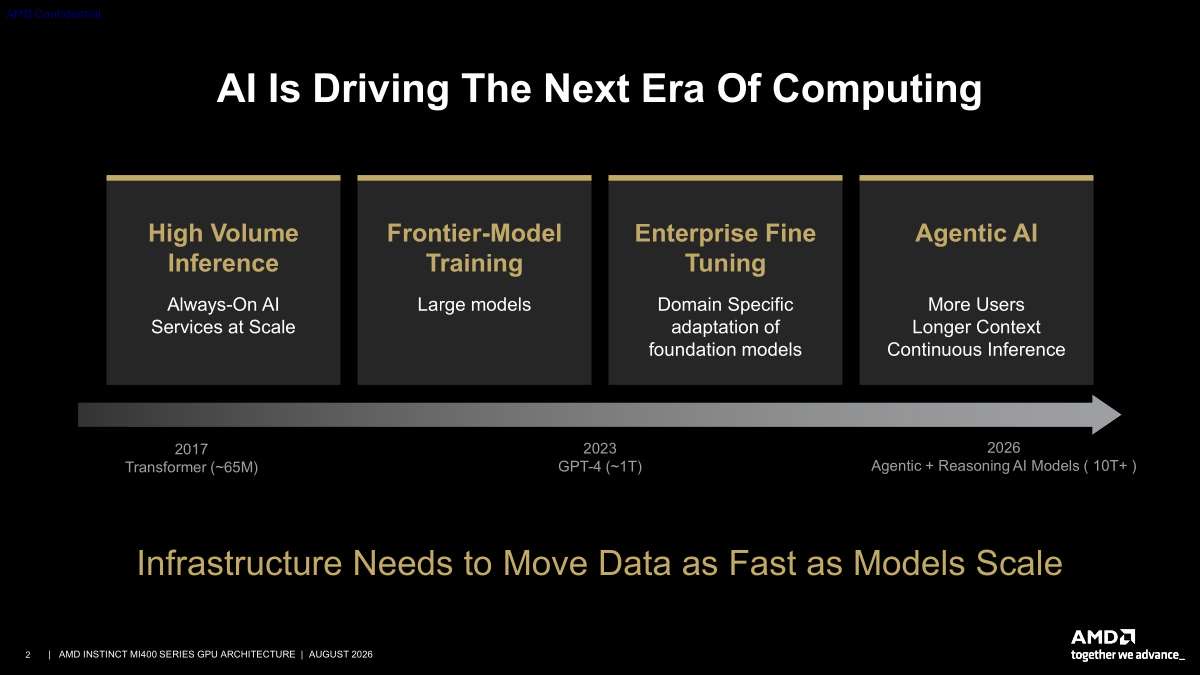 图01|Slide 2: AI Is Driving The Next Era Of Computing
AMD frames the MI400 family around Helios, the rack-scale AI infrastructure it expects to ship. Headline numbers are a 2.9 exaflop rack with 31 TB of HBM4 memory and 1.7 PB/s of HBM4 bandwidth across 72 GPUs, along with 260 TB/s of scale-up and 43 TB/s of scale-out bandwidth per rack. We have covered AMD’s double-wide Helios racks before, and this fills in the silicon behind them.
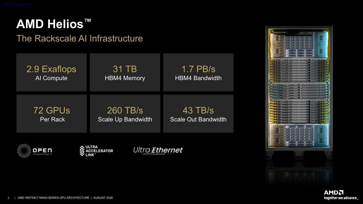 图02|Slide 3: AMD Helios — 2.9 EFLOPS、31TB HBM4、72 GPU
This basic building block is a compute tray that combines compute, host CPU, memory, and networking. Each tray holds four AMD Instinct MI455X EAMs fed by a single-socket AMD EPYC 9006 SP7 server CPU over Infinity Fabric, with UALoE links carrying scale-up traffic at 1.8 TB/s per direction per GPU and up to three AMD Pensando Vulcano 800 AI NICs per EAM handling scale-out.
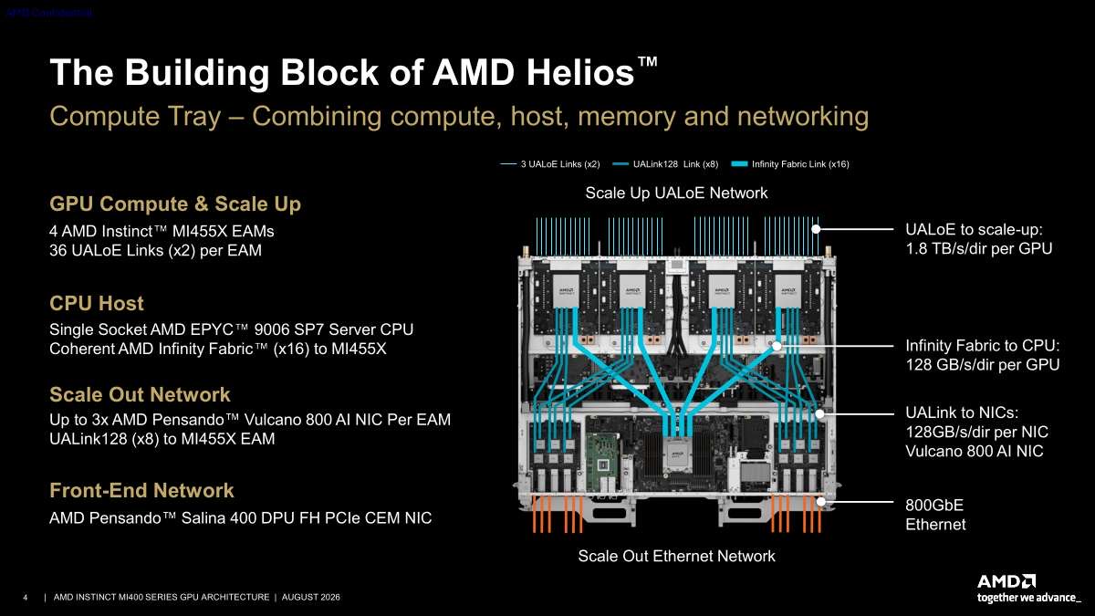 图03|Slide 4: The Building Block of AMD Helios
Here you can see the Helios node from Advancing AI 2026:
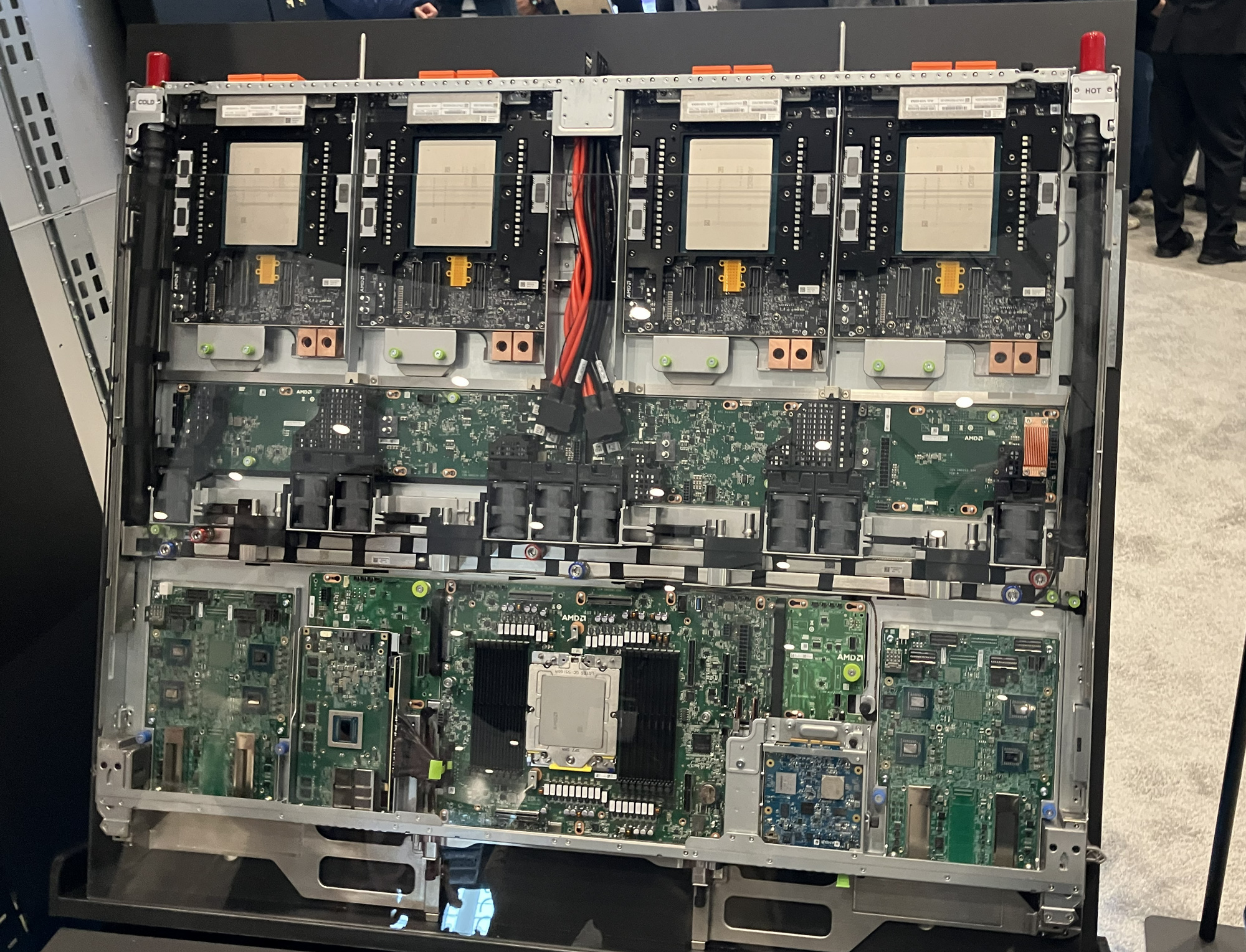 图04|Helios Compute Tray Uncapped
At the center of the tray is the AMD Instinct MI455X, an enhanced modular chiplet design built from eight accelerator complex dies on N2 flanked by fabric and cache dies plus I/O dies on N3P. It packages 256 total active work group processors with 192 MB of global L2 and 12x HBM4 stacks running 432GB at 23.3 TB/s, and it connects through PCIe Gen 6 as well as 72 UALoE lanes pushing 3.6 TB/s. We have a full AMD Instinct MI455X and CDNA 5 deep dive for more on the GPU.
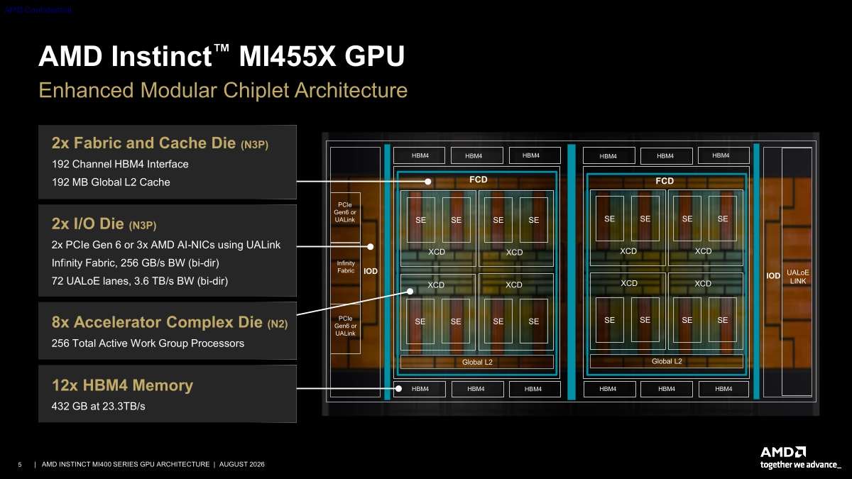 图05|Slide 5: AMD Instinct MI455X GPU — 8×N2 XCD + N3P fabric/IO die
This packaging split is notable because each die type moves to the node that best fits its job. Compute dies on N2 sit under 3D hybrid-bonded XCDs for higher density per watt, while the N3P fabric, cache, and I/O dies, plus CoWoS-L packaging, tie the whole package around the twelve HBM4 stacks.
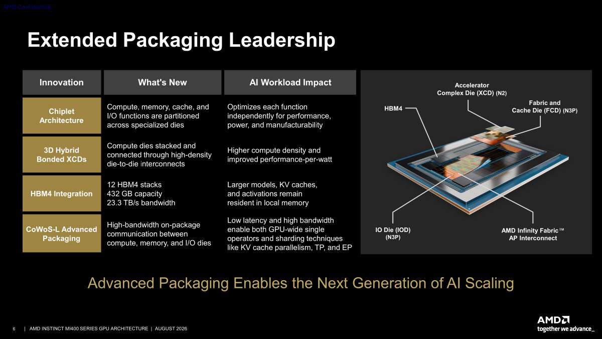 图06|Slide 6: Extended Packaging Leadership
AMD boils the MI400 changes into three buckets: bigger memory and cache, faster compute, and less data movement.
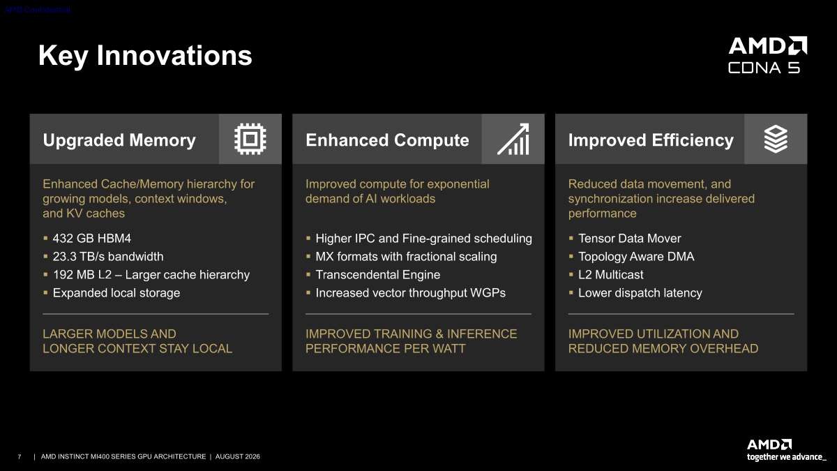 图07|Slide 7: Key Innovations
AMD has its conceptual block diagram. It is useful for keeping the XCDs, fabric and cache dies, I/O dies, and HBM4 stacks straight as AMD walks through how scale-up and scale-out attach to the package. One of the challenges with this approach is ensuring you can get power to all of the dies as well as just cooling them.
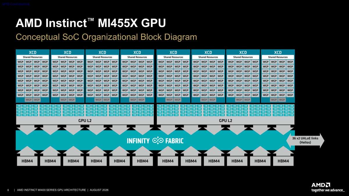 图08|Slide 8: AMD Instinct MI455X 概念框图
The new MI455X substantially expands the on-chip memory hierarchy compared to the MI355X. AMD doubles per-SIMD vector registers and per-WGP local data share, and a 4 MB L2 broadcast arbitrator can amplify bandwidth by up to 4x. Main memory jumps from 288 GB of HBM3E to 432 GB of HBM4, a 1.5x capacity increase, while AMD lists roughly 2.9x the total HBM bandwidth. The L2/Infinity Cache changes are a big one that AMD has focused on previously since that is an area that was re-architected in the SoC.
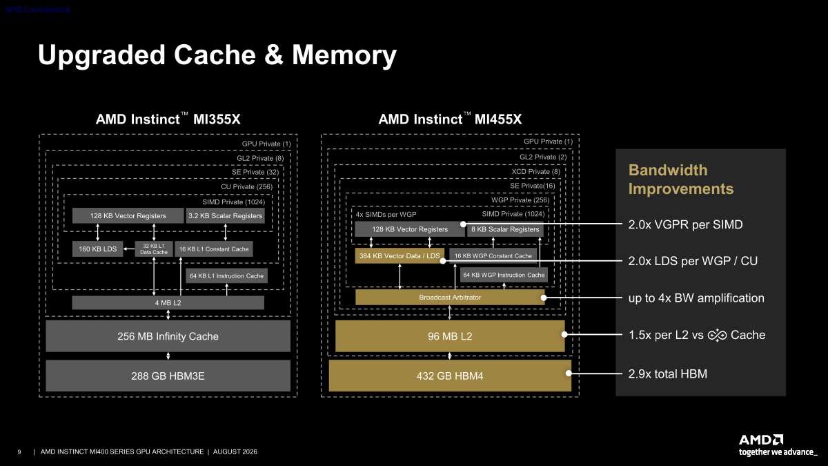 图09|Slide 9: Upgraded Cache & Memory
On the compute side, the headline is a peak MXFP4 figure of 40.26 petaflops, up to 4x the MI355X, with MXFP6 and MXFP8 each rated at 20.13 petaflops. Vector FP16 and matrix or vector FP32 both reach 315 TF, up to 2x, on a 256 WGP architecture. Native Wave32 execution and a new transcendental engine target lower dispatch latency and faster attention math.
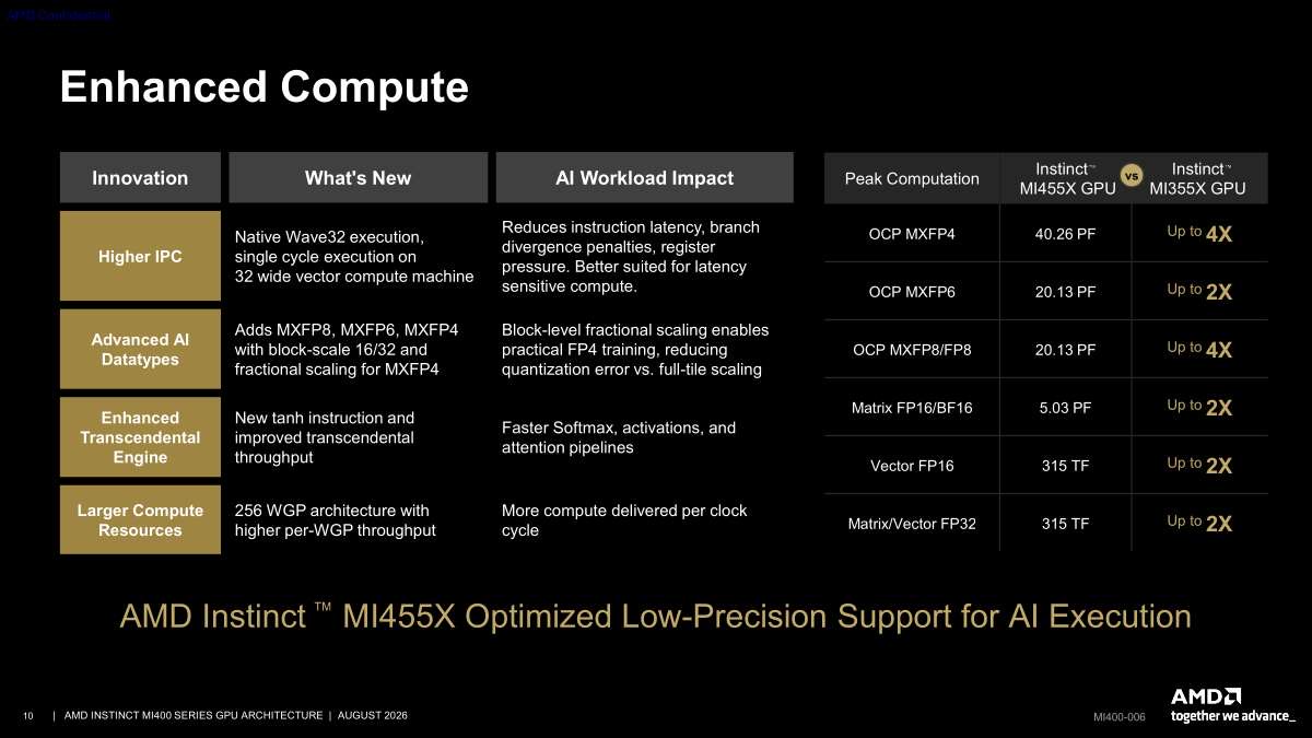 图10|Slide 10: Enhanced Compute
AMD walks through the MX data formats it is adopting across the stack. This table lays out exponent and mantissa layouts from float64 down through the MXFP family, with shared-scale blocks that can now span 16 or 32 elements and a new fractional scale for MXFP4. Four-bit tensor LUT instructions let data stay in 4-bit memory and convert to 4, 6, or 8-bit compute formats.
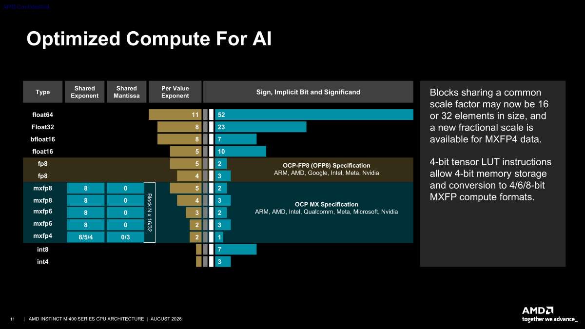 图11|Slide 11: Optimized Compute For AI — MX 格式全家桶
This efficiency push is about keeping work and data in place. A Tensor Data Mover copies data asynchronously into local LDS without staging through registers, work group clusters, and L2 multicast cuts redundant traffic for operators like GEMM and Flash Attention, and a reworked command processor lowers dispatch latency so short kernels stay fed.
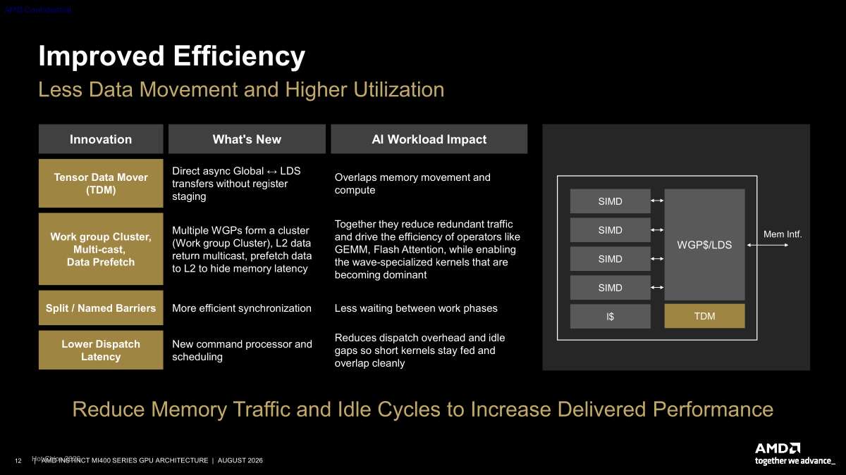 图12|Slide 12: Improved Efficiency
AMD moves data movement into dedicated DMA engines so transfers run in parallel with AI kernels instead of stealing compute cycles. Topology-aware HBM DMA automatically affinitizes traffic to UALoE links, which keeps software oblivious to data placement and spreads load across the 72-GPU fabric.
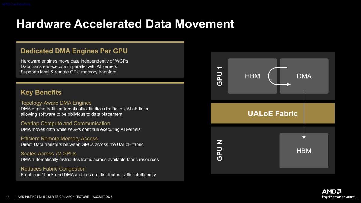 图13|Slide 13: Hardware Accelerated Data Movement
Software is where AMD is trying to narrow the ROCm gap. It positions the ROCm core framework as the integration point and is shipping AI Skills so popular agents such as Claude, Codex, Cursor, and Gemini become ROCm users, plus a Hyperloom tool for end-to-end workload optimization.
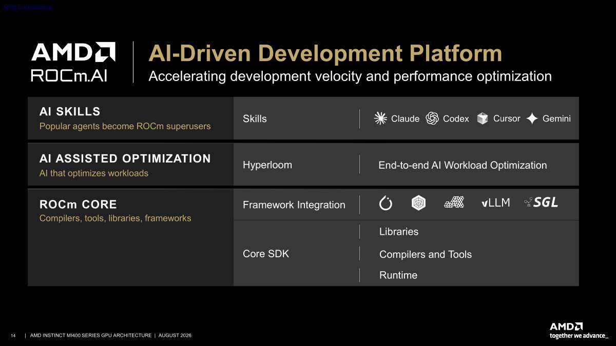 图14|Slide 14: AI-Driven Development Platform
AMD closes the architecture section with ROCm.AI performance comparisons of the MI455X against the MI355X. It reports 20 TB/s of measured MLA decode bandwidth in FP8 for 3.8x higher performance, 20 petaflops of measured FP4 compute for 3.3x higher AI compute, 3.2 TB/s of scale-up bandwidth for 3.5x higher bandwidth, and 190 GB/s of scale-out bandwidth for 2x higher bandwidth. AMD also estimates a 2.4x gain in AI energy efficiency on the way to its 2030 goal of a 20x improvement in rack-scale efficiency.
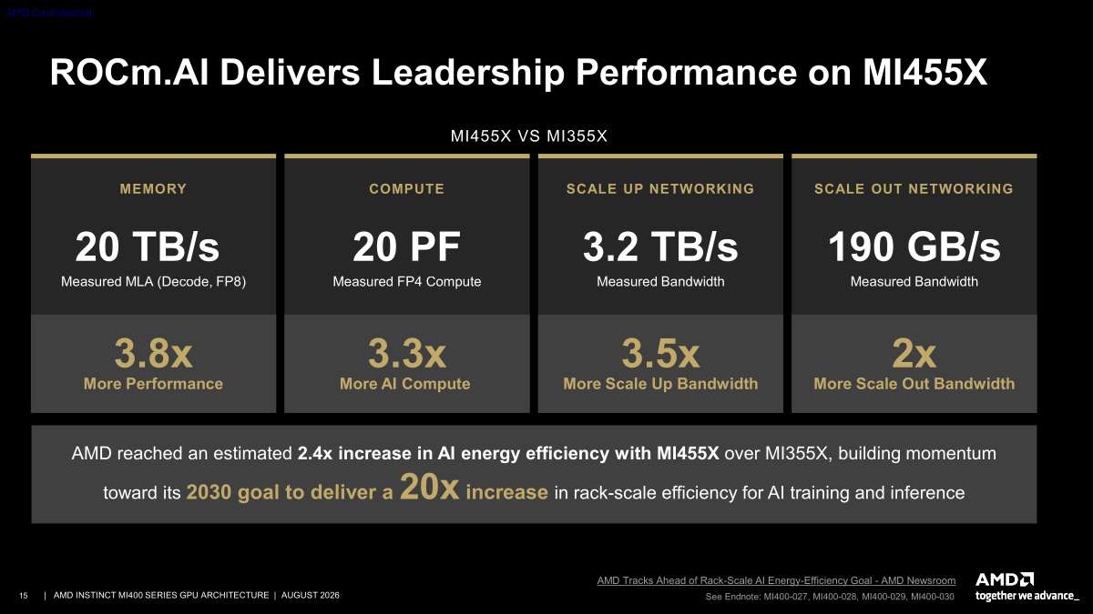 图15|Slide 15: ROCm.AI Delivers Leadership Performance on MI455X
AMD wraps up with the six threads it says carry the future of AI, from advanced packaging with SOIC, HBM4, and CoWoS-L, through fault-tolerant memory and confidential computing, to the 72-GPU rack-scale subsystem and a modular architecture built for frontier training and high-volume inference.
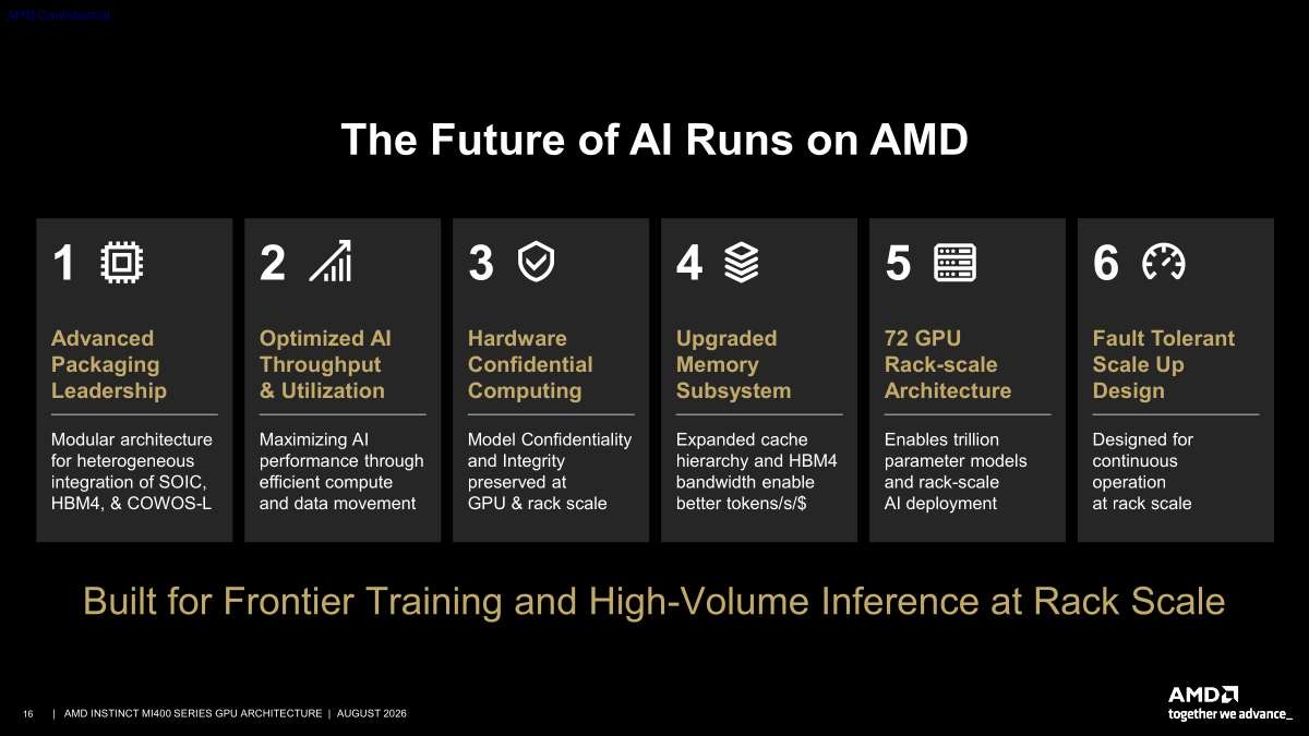 图16|Slide 16: The Future of AI Runs on AMD
It is a dense presentation, but the through-line is clear. AMD pairs a substantially larger memory and compute envelope in the MI455X with the Helios rack fabric and a software stack designed to ease the CUDA migration.
Final Words
Since we have Ryan’s deep-dive, that is probably still the best resource, but it was good to see at Hot Chips 2026 as well. A lot of folks in the room here are different than they were in San Francisco a few weeks ago. AMD has a big GPU for this generation in the Instinct MI455X.
第二部分:解析(深度解读)
核心论点摘要
AMD 在 Hot Chips 2026 上把 MI455X 定位为 Helios 机架的硅引擎,全场叙事围绕「为机架规模系统而生的巨型 GPU」:
- 芯片规格:8 颗 N2 计算 die(XCD,3D 混合键合堆叠)+ N3P fabric/缓存/IO die + CoWoS-L 封装 + 12 堆 HBM4(432GB @ 23.3TB/s);256 WGP、192MB 全局 L2、72 条 UALoE lane(3.6TB/s)、PCIe Gen6。
- 算力跃升:MXFP4 峰值 40.26 PFLOPS(对 MI355X 最高 4 倍);实测口径:MLA decode 带宽 20TB/s(3.8x)、FP4 计算 20 PFLOPS(3.3x)、scale-up 3.2TB/s(3.5x)。
- Helios 机架整体:72 GPU、2.9 EFLOPS、31TB HBM4、1.7PB/s HBM 带宽、260TB/s scale-up、43TB/s scale-out——AMD 明确以「机架」为单位与 NVIDIA 对垒。
- 数据搬运成为独立创新轴:Tensor Data Mover(绕过寄存器直写 LDS)、L2 多播、拓扑感知 HBM DMA(自动亲和 UALoE)——「让数据不动」与「让数据搬运硬件化」并举。
关键概念解读
- 按 die 功能选工艺节点:计算 die 用 N2(密度/能效优先),fabric/IO die 用 N3P(成本/成熟度优先)——chiplet 架构下「异构节点组合」已是标准打法,与 NVIDIA Rubin 的多 die 划分思路趋同。
- MXFP4 与 LUT 指令:4-bit 数据驻留内存,经查表转换成 4/6/8-bit 计算格式——低精度数据通路是 40 PFLOPS 数字的来源,实际收益取决于工作负载对精度的容忍度。
- ROCm 的 AI Skills 策略:让 Claude/Codex/Cursor/Gemini 等 AI agent 直接成为 ROCm 用户——用 AI agent 的采纳曲线弥补 CUDA 生态差距,是一个低成本高杠杆的软件叙事。
分层拆解表
| 维度 | MI355X(上一代) | MI455X(本代) | 倍数 |
|---|---|---|---|
| 显存容量 | 288GB HBM3E | 432GB HBM4 | 1.5x |
| HBM 带宽 | ~8TB/s | 23.3TB/s | ~2.9x |
| 峰值低精度算力 | ~10 PFLOPS | 40.26 PFLOPS (MXFP4) | 最高 4x |
| Scale-up 带宽/GPU | ~0.9TB/s | 3.2TB/s(UALoE 实测) | 3.5x |
| 机架口径 | — | 2.9 EFLOPS / 31TB / 1.7PB/s | 72 GPU Helios |
技术趋势判断
MI455X 与 NVIDIA Rubin(见本站《NVIDIA Vera Rubin NVL72 机架》)在同一届 Hot Chips 上分别交卷,竞争单位都已从「芯片」升格到「机架/工厂」:AMD 讲 2.9 EFLOPS 机架 + UALoE 以太网 scale-up,NVIDIA 讲 100MW AI Factory 口径的 2 ZFLOPS。两者的共同底座是 HBM4 × 12 堆 + 先进封装(CoWoS-L / SOIC)+ 3D 混合键合——先进封装与存储供应商是这场军备竞赛的确定性受益方。AMD 的差异化赌注在 UALoE 开放生态与 ROCm 迁移成本,短板仍是软件实测生态。
风险提示
AMD 提供的性能倍数多为理想口径(峰值/实测混合,实际部署受制于软件栈成熟度与整机功耗约束);Helios 72-GPU scale-up 域的良率与交付节奏未经第三方验证;ROCm 与 CUDA 的差距收敛速度存在不确定性。本文不构成投资建议。