Taiwan GTC (Computex 2026): CPO Just Entered Production, So Why Are Coherent and Lumentum, the Companies It Was Supposed to Kill, Still on the Supplier List? — 台湾、GTC 与 Computex 2026:CPO 已进入量产
整理 PhotonCap 关于 NVIDIA Spectrum-X 光电共封装(CPO)在 Computex 2026 进入量产的英文原文,并附中文深度解读,拆解 CPO 供应链、被吞噬与被新增的光学内容,以及投资含义。
本文整理自 PhotonCap(photoncap.net),原文发布于 Jun 04, 2026(标题原文:Taiwan GTC (Computex 2026): CPO Just Entered Production, So Why Are Coherent and Lumentum, the Companies It Was Supposed to Kill, Still on the Supplier List?)。 结构为 正文(英文原文)+ 解析(中文深度解读),方便中英对照阅读。 来源说明:内容经公开页面获取;本发布保留完整英文原文并附中文深度解读,仅作信息整理与学习用途,著作权归原作者所有,建议在原站支持作者订阅。 ⚠️ 本文含付费段落,以下仅发布公开可读部分;付费深解未包含。
第一部分:正文(Original Article)
Taiwan GTC (Computex 2026): CPO Just Entered Production, So Why Are Coherent and Lumentum, the Companies It Was Supposed to Kill, Still on the Supplier List?
$NVDA $COHR $LITE $GLW $FN $TSM | Spectrum-X Photonics Goes Production: The CPO Supply Chain
On May 31, 2026 (US press release date, Taiwan GTC Taipei keynote), NVIDIA called Spectrum-X Ethernet Photonics “now in production.” It is the world’s first co-packaged optics (CPO) Ethernet switch built on 200G SerDes, with CoreWeave, Lambda, and Oracle Cloud Infrastructure among the first adopters. One caveat up front: “now in production” marks the start of a manufacturing ramp, while broad availability is guided to the second half of 2026, so the two should be read separately. CPO pulls optical I/O right next to the switch silicon, so the market’s first reaction was pluggable transceiver cannibalization. Yet on the 11-partner supply chain list NVIDIA disclosed back in 2025, the very companies that build pluggables (Coherent, Lumentum) show up again as CPO suppliers. This piece looks at who actually builds what behind that one-line “production” claim, and how cannibalization and upside can happen inside the same company at once.
Contents
- Intro: NVIDIA Put Money Into the Companies It Was Supposed to Kill
- Where CPO Actually Landed: Scale-Out, Not Scale-Up
- The Three Physics Problems That Blocked Production
- The Question to Ask After “Production”
- Splitting the 11 Suppliers by Role
- Cannibalization vs Content, Inside One Company
- Fiber: The Second Set of Numbers CPO Creates
- Where the Real Chokepoint Is
- Scenarios, Monitoring Points, Close
- References & Sources
1. Intro: NVIDIA Put Money Into the Companies It Was Supposed to Kill
The market read CPO as the death of the pluggable transceiver. NVIDIA, instead, put money into the suppliers that were supposedly dying. In 2026 it invested $2B each into Coherent and Lumentum on March 2 [9], $2B into Marvell at the end of March [10], and tied Corning in directly in May [6]. The stranger part: on the Spectrum-X Ethernet Photonics supply chain list NVIDIA disclosed back in 2025, Coherent and Lumentum are already there. The supposed casualties are also suppliers to the new platform.
That contradiction is where this piece starts. CPO removes the pluggable form factor, not the optical content. It unbundles the economics that used to sit inside one transceiver module into three layers: the laser that makes the light, the fiber and connectors that move it, and the packaging that bonds the electronic and photonic chips. So the question for an investor is not “how much pluggable does CPO kill,” but where the dollars from the shrinking transceiver socket get captured again. I broke down which layer each of the four investments targeted in a prior piece, “Coherent, Lumentum, Marvell, and Now Corning”.
Now the event itself. On May 31, 2026 (US press release date), at the Taiwan GTC Taipei keynote, NVIDIA said the Vera Rubin platform had entered full production, and inside that was one line. Spectrum-X Ethernet Photonics is “now in production,” into its manufacturing ramp, with CoreWeave, Lambda, and Oracle Cloud Infrastructure among the first adopters [1][2]. The Ethernet version that was “expected in 2026” at GTC in March 2025 [3] has flipped to “in production.”
Takeaway: what changed is one word (”expected” to “in production”), but while the market asks “who dies,” NVIDIA had already lined up “who gets paid again in a different layer.”
2. Where CPO Actually Landed: Scale-Out, Not Scale-Up
Read CPO as nothing more than “swap all copper for optics” and the market’s read-through goes wrong. The first thing to pin down is exactly which links this product replaced.
Connections inside an AI rack come in two kinds: scale-up, which binds GPUs together inside a rack, and scale-out plus scale-across, which link rack to rack and site to site. In the Vera Rubin NVL72, scale-up runs on the sixth-generation NVLink Switch and stays copper [2], while the Spectrum-X Ethernet Photonics that just entered production handles the scale-out and scale-across Ethernet fabric alongside the ConnectX-9 SuperNIC [2]. CPO did not strip copper out of the rack interior. It went into the fabric leaving the rack first.
Why can scale-up stay copper while scale-out has to go optical? It comes down to distance and frequency. Copper loss climbs steeply as signal frequency rises. As lane rates climb toward 200G SerDes, the distance over which copper can still recover the signal shrinks. Inside a rack, GPU to GPU (scale-up) is typically within 1 to 2 meters, so copper still closes the link at these rates, and it beats optics on power, latency, and cost. But rack to rack and site to site (scale-out and scale-across) stretch from several meters to tens or hundreds of meters, and at those distances copper falls into a loss regime that equalization cannot rescue. Fiber, by contrast, is a medium whose loss is measured per kilometer, so it carries long distances at low loss. That is why scale-out is forced optical. And as lane rates rise, the distance copper can hold shrinks, pushing optics closer to the chip. CPO is where that push lands.
Why this distinction matters: “CPO kills NVLink copper” and “CPO replaces part of the scale-out Ethernet pluggable market” are claims of completely different size. What happened now is the latter. The former has not.
On the spec sheet, each port is 1.6 Tb/s, and depending on configuration the switch spans 102.4 Tb/s (128 ports of 800G) to 409.6 Tb/s (SN6800, 512 ports of 800G or 2,048 ports of 200G) [5][7]. (NVIDIA’s 2025 press release rounded these to 100/400 [3].) The efficiency figures use different baselines across announcements. The 2025 platform launch cited, versus traditional designs, 3.5x energy savings, 63x signal integrity, 4x fewer lasers, 10x resiliency, and 1.3x deployment [3], while the Spectrum-X Ethernet Photonics technical material cites, versus pluggables, 5x power per port, 5x AI uptime, and 10x resiliency [7]. Both are company figures with different baselines, and neither is independently verified.
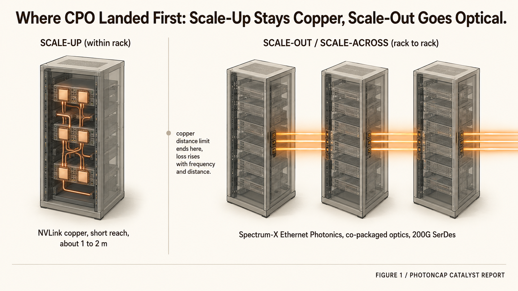
Takeaway: CPO did not “rip all copper out of the rack.” It “went into the fabric leaving the rack first.” That difference sets the boundary of cannibalization.
3. The Three Physics Problems That Blocked Production
CPO sat at “maybe” for years not because the idea was hard, but because three physics problems blocked production. That these three reached a level where they integrate within a production configuration is what “now in production” actually means. Yield, per-customer qualification, and long-term reliability are separate items to keep watching.
First, where to make the light. Silicon passes light well but cannot generate it, so the laser source sits outside the package (External Laser Source, ELS) and its light is fed into the silicon photonics engine. Put the laser right next to the chip and heat destroys it. Assembling, optically aligning, and testing this ELS is the first hard problem [4].
Second, how to couple that light in without loss. Light from the external laser has to be coupled into the silicon photonics engine while preserving polarization, and the processed signal has to exit through front-panel fiber. This is a precision problem for optical connectors and fiber assemblies [4].
Third, how to stack the electronic and photonic chips in one package. Long electrical paths cost efficiency, so the electronic IC (EIC) has to sit directly on top of the photonic IC (PIC) in 3D. That is what TSMC’s COUPE process does [4][5].
None of the three is the kind one company solves alone. The laser maker, the fiber-coupling specialist, and the 3D-stacking foundry are each different. That the layers have different owners is the starting point for the investment view.
Takeaway: CPO production = external laser (ELS) + fiber coupling + 3D packaging, with all three layers meshing together in a production configuration. Different owners per layer is where the investment view begins.
4. The Question to Ask After “Production”
Up to here is the range anyone can see by following the press release and the technical blog. What the public release tells you is that the switch exists. The investable part is next: splitting the 11 disclosed suppliers by role.
The question narrows to this. Among these 11, who gains new content and who gives up a socket? Do Coherent and Lumentum gain more from ELS lasers than they lose from pluggables, or less? Why does Corning have its own separate arithmetic? And which single spot, if it falls out, stops the line?
Production is a start signal, not a destination. Between the announcement, volume shipment, and a meaningful attach rate sit more gates of yield and qualification, and at each gate a different layer books revenue first. Below: the 11-supplier split, the net of cannibalization and upside, the chokepoint, and scenarios.
第二部分:解析(深度解读)
一、这篇文章为什么重要
这篇 PhotonCap 文章的价值,不在于又复述了一遍「NVIDIA 说 CPO 量产了」的新闻,而在于它用一条供应链的视角,戳破了市场最容易陷入的两个误读:
第一,把「CPO 量产」读成了「可插拔光模块死刑」。原文开宗明义:CPO 去掉的是 pluggable form factor(可插拔形态),不是 optical content(光学内容)。换句话说,光模块里原本打包在一起的经济价值,被拆成了三层——产生光的激光源、搬运光的光纤与连接器、把电芯片和光芯片键合在一起的封装。形态消失不等于需求消失,只是钱从「一个模块」流向了「三条供应链」。
第二,把「进入量产」读成了「全面可用、全面替代」。原文在开头就给了关键 caveat:「now in production」只是制造爬坡的起点,而「broad availability」被指引到 2026 年下半年。这是两个必须分开读的信号。对投资者而言,这意味着真正的营收兑现还要穿过良率(yield)、客户认证(per-customer qualification)与长期可靠性这几道仍未关闭的闸门。
文章的另一个稀缺点,是它把 NVIDIA 在 2026 年的几笔投资串成了一条逻辑线:3 月 2 日向 Coherent、Lumentum 各投 20 亿美元,3 月底向 Marvell 投 20 亿美元,5 月又把 Corning 直接绑进供应链。曾被市场判定为「被 CPO 杀死」的公司,恰恰是 NVIDIA 亲自下注、并早已列在 2025 年那份 11 家供应商名单上的对象。这个反差,正是全文的投资主线。
二、核心论点拆解
可以把文章的论证拆成如下几层:
| 层次 | 原文论点 | 投资含义 |
|---|---|---|
| 叙事反差 | 市场把 CPO 当可插拔模块的终结者;NVIDIA 反而重金投资 Coherent / Lumentum / Marvell / Corning | 「谁死」是错的问题;问题是「钱在哪一层的插座里被重新捕获」 |
| 形态 vs 内容 | CPO 取消的是模块形态,不是光学内容;价值被拆成 激光 / 光纤连接器 / 封装 三层 | 同一家公司可以同时「失去插座」又「获得内容」 |
| 落地位置 | CPO 落在 scale-out / scale-across(机柜间、站点间)的以太网 fabric,而非机柜内 scale-up 的 NVLink 铜线 | 被替代的是 scale-out 可插拔市场的一部分,NVLink 铜互连毫发无伤 |
| 量产真义 | 「量产」= ELS 外置激光 + 光纤耦合 + 3D 封装(TSMC COUPE)三者在同一生产配置中咬合 | 三层各有不同 owner,投资视角由此展开 |
| 后续追问 | 11 家供应商谁增内容、谁让出插座?Coherent/Lumentum 的 ELS 增益能否盖过可插拔损失?Corning 为何有独立算式?哪里是单点 chokepoint? | 这些问题落在付费部分(05–10 节),是本文被付费墙截断之处 |
一句话总结原文的骨架:「expected → in production」只改了一个词,但市场问「谁死」,NVIDIA 早已排好「谁在另一层再次收钱」。
三、关键概念 / 技术解读
1. CPO 与 200G SerDes。 Spectrum-X Ethernet Photonics 是全球首个基于 200G SerDes 的 CPO 以太网交换芯片。SerDes(串行器/解串器)的 lane rate 越高,铜线能「救回信号」的距离越短——这正是 CPO 被迫靠近芯片的物理根源。原文给的量化锚点是:机柜内 GPU 到 GPU(scale-up)通常 1–2 米,铜线仍能闭环且更省功耗、更低延迟、更便宜;而机柜间到站点间(scale-out / scale-across)从数米延伸到数十、上百米,铜线落入均衡(equalization)无法挽救的损耗区间,光纤则按每公里计量损耗、长距离低损。
2. Scale-up vs Scale-out(这是全文最重要的区分)。 在 Vera Rubin NVL72 里,scale-up 走第六代 NVLink Switch、仍然是铜;而刚刚量产的 Spectrum-X 光电方案,与 ConnectX-9 SuperNIC 一起,负责 scale-out / scale-across 的以太网 fabric。结论很清楚:CPO 没有把机柜内的铜「拔掉」,而是「先进入离开机柜的那张 fabric」。因此「CPO 杀死 NVLink 铜线」和「CPO 替代一部分 scale-out 以太网可插拔市场」是体量完全不同的两句话——现在发生的是后者,不是前者。
3. 三道挡住量产的物理题。(a)光从哪来:硅能传光但不能发光,激光源必须放在封装外(External Laser Source, ELS),再把光喂进硅光引擎;激光紧贴芯片会被热毁掉,ELS 的组装、光学校准与测试是第一道难题。(b)如何无损耦合:外置激光的光要在保持偏振的前提下耦合进硅光引擎,处理后信号还要从前面板光纤出射,这是光纤组件与连接器的精密难题。(c)如何 3D 堆叠:长电通路损耗效率,所以 EIC 必须 3D 直接叠在 PIC 之上——这正是 TSMC 的 COUPE 工艺干的事。这三层没有一家能单独解决,于是「不同层归不同 owner」成了投资视角的起点。关于 COUPE/3D 堆叠,可参考 TSMC 在 CPO 上领先、三星为第三芯片;关于外置激光源(ELS)的激光技术,可参考 CPO/NPO 激光(一):InP 与 (二):Lumentum 的技术与护城河。
4. 规格与效率数字(注意基线)。 每端口 1.6 Tb/s;按配置不同,交换容量从 102.4 Tb/s(128×800G)到 409.6 Tb/s(SN6800,512×800G 或 2048×200G);2025 年新闻稿曾舍入为 100/400 Tb/s。效率数字跨公告基线不一致:2025 平台发布称相对传统设计 3.5× 节能、63× 信号完整性、4× 更少激光、10× 弹性、1.3× 部署;Spectrum-X 技术材料则称相对可插拔 5× 单端口功耗、5× AI 在线时长、10× 弹性。两者都是公司口径、基线不同、均未独立验证——读的时候不能把两组数字直接相加或混用。
四、与本站其他 CPO / 硅光系列文章的链接
- CPO 最大的瓶颈:高良率测试 —— 直接对应原文「量产之后仍有 yield / 客户认证闸门」的提醒,是判断营收何时真正兑现的关键。
- TSMC 在 CPO 上领先、三星为第三芯片 —— 对应原文第三道物理题中的 TSMC COUPE 3D 堆叠工艺。
- CPO/NPO 激光(一):InP 与 (二):Lumentum 的技术与护城河 —— 对应原文的 ELS 外置激光源,以及 Coherent / Lumentum 为何仍是 CPO 供应商。
- CPO 的幻觉(CPO 特别篇终章) —— 与本文「CPO 不是可插拔模块的简单死刑」的叙事形成呼应。
五、投资意义
明确点名的标的(原文含 tickers): $NVDA、$COHR(Coherent)、$LITE(Lumentum)、$GLW(Corning)、$FN(Fabrinet?原文未展开)、$TSM(台积电)。
- Coherent / Lumentum($COHR / $LITE):被吞噬与被新增并存。 市场第一反应是「可插拔模块被 CPO 吃掉 → 这两家要完」。但原文指出它们早已在 2025 年的 11 家供应商名单上,且 NVIDIA 2026 年各投 20 亿美元。核心问题变成:它们在 ELS 激光上「新增的内容」能否盖过在可插拔上「失去的插座」?这正是付费部分(06 节)要算的账。对投资者,关键不是「CPO 利空 COHR/LITE」的线性故事,而是净敞口方向。
- Marvell($MRVL,原文以 $ 形式但列名): 3 月底获 20 亿美元投资,对应三层中「电芯片 / 交换 / 串行器」一侧。
- Corning($GLW): 5 月被直接绑进供应链,且原文强调它「有自己独立的一套算式」——指向光纤与连接器(三层中的第二层)在 CPO 下被放大的用量,这部分在付费部分(07 节「Fiber: The Second Set of Numbers」)展开。
- 台积电($TSM): COUPE 工艺是 3D 堆叠(EIC-on-PIC)的承载者,是「第三道物理题」的解决方,确定性相对高。
- 下游云厂: CoreWeave、Lambda、Oracle Cloud Infrastructure 被列为首批采用者,是需求侧验证信号。
一句话投资框架: CPO 不是「消灭一层、利好另一层」的零和,而是「形态消失、内容三层重分配」,在同一个公司内吞噬与增量可以同时发生。
六、风险提示
- 量产 ≠ 全面可用: 「now in production」只是爬坡起点,broad availability 指引到 2026 下半年;其间还有良率、客户认证、长期可靠性三道未关闭的闸门(原文明确列为需持续观察项)。
- 效率数字为公司口径、未独立验证: 3.5×/63×/5× 等数字跨公告基线不同,不能直接外推或相加。
- 付费部分含关键结论: 11 家供应商的角色拆分、吞噬与增量的净额、真正 chokepoint 与情景分析(05–10 节)均在付费墙之后,本文仅含公开免费部分,相关定量判断请以原站付费内容为准。
- 单点依赖风险: 原文点出「哪一个环节掉链子就会停线」是核心监控点,但结论在付费部分——任一层的供应集中(ELS 激光、光纤耦合、COUPE 封装)都可能成为瓶颈。
- 时间窗与定价: 原文附带了 6 月 3 日生效的订阅调价信息,属作者商业动作,与基本面无关,不应混入投资判断。
以上解读基于原文信息整理,不构成投资建议。