硅光代工层:谁真的能造出一颗 PIC —— PhotonCap × Crack The Market 深度报告精读
把 2026 年硅光代工层的六家玩家、三条错价、2028 年的产能碰撞与底下的衬底垄断画成一张地图;附英文原文全文与 20 张原图。
来源:PhotonCap × Crack The Market(Ozeco)联合深度报告,原文发布于 2026 年 9 月。 原文:The Silicon Photonics Foundry Layer: Who Can Actually Make a PIC — https://photoncap.net/p/the-silicon-photonics-foundry-layer 原文涉及的标的:Tower(TSEM)、GlobalFoundries(GFS)、TSMC(TSM)、STMicroelectronics(STM)、UMC、Soitec(SOI)——原文列举,非本站推荐。 转载说明:第一部分为英文原文完整转载,含原文全部 20 张配图(图注为本站所加中文说明),版权归原作者所有;本站仅调整排版与标题层级、将原文内嵌超链接转为纯文本,不改动任何文字表述。第二部分为本站独立撰写的中文结构化解读,其中的质疑与判断属解读者观点,不构成投资建议。
第一部分:英文原文(Original Article)
This piece puts together two perspectives that rarely sit side by side: Crack The Market’s top-down view of market structure and where the investment opportunity sits, and PhotonCap’s engineering-level view of how photonic chips are built, bonded and tested. Together we have mapped a layer of the optical stack that has received surprisingly little attention: the foundries that actually fabricate the PICs (photonic integrated circuits) running through every AI optical link.
Crack The Market owns the substrates, materials, the European layer and the demand side. PhotonCap owns the foundries, the Asian ecosystem and packaging. Put the two together and one argument runs through the entire piece: the optical transition is consensus, the scarce asset is the capacity to fabricate the PIC, and the scarcer asset is the wafer it is fabricated on.
Six companies sit on that map, and the merchant suppliers among them are being paid, or asked to be paid, before they build. Tower’s customer advances and deferred revenue stood at about $320m at the end of June, and STMicroelectronics says customers are asking for long-term agreements with cash advances, per Investing.com’s transcript.
Seen from the packaging bench, the step that paces co-packaged optics (CPO), where the optical engine sits inside the switch package, comes after the wafer is made. In TSMC’s flow the driver die is stacked onto the photonic die with SoIC-X, a solder-free bond made copper pad to copper pad that cannot be reworked, and Nvidia uses only known-good engines, so each engine is screened before it is mounted. TrendForce lists optical engine yield and advanced packaging capacity beside silicon photonics fabrication among the limits on the CPO ramp. That bond, and the optical test that follows it, is the step PhotonCap watches most closely.
Executive Summary
The market has spent 2026 pricing the lasers. It has not yet mapped the layer that turns those lasers into links: the six foundries that can fabricate a silicon photonics PIC at scale. The layer is not unknown, it is unmapped, and that has created mispricing.
Three mispricings fall out of the map. STMicroelectronics is a merchant PIC supplier at roughly Tower’s scale, yet it does not appear on most foundry maps. GlobalFoundries’ claim to be the largest pure-play photonics foundry has already been overtaken by Tower on revenue. TSMC is usually modelled as a merchant foundry, but sells photonics only through its own SoIC bonding line.
Scarcity has already turned into prepayments. Tower took $290m in a single quarter to reserve 2027 capacity. STMicroelectronics is signing long-term agreements with cash advances. Soitec is signing multi-year reservation agreements with eight of its roughly ten major Photonics-SOI customers.
The layer splits by form factor, not technology. Pluggables are a merchant market, with three suppliers taking prepayments. Co-packaged optics is a captive market, with one supplier allocating bonding slots. Near-packaged optics is the contested middle, and it will determine where much of the value lands from 2028.
2028 is when the capacity wave arrives. Four merchant 300mm expansions are due to come through around the same period. On our base-case arithmetic, Tower’s Japan programme alone exceeds the industry’s 2030 wafer requirement. The risk is therefore wafer pricing, not fab capacity, and Tower’s CFO identifies it as the largest variable in its model.
Every one of those fabs leads back to the same substrate supplier. Soitec holds roughly 95% of 300mm Photonics-SOI and has guided the business to 2.5-3x last year’s level. Every 300mm expansion in this piece is, ultimately, a Soitec order.
The bottlenecks are not equally scarce. Our ranking, from hardest to substitute to easiest, is the substrate, InP lasers, SoIC bonding, merchant wafer starts and finally the epitaxy tools.
The conclusion is simple: the scarce asset is the capacity to fabricate the PIC. The scarcer asset is the wafer it is fabricated on.
Before this deep dive, I recommend reading some of our other write ups on the AI & Technology megatrend, and PhotonCap’s pieces that this collaboration builds on:
The investment case for the substrate every foundry in this piece buys from, and why the Photonics-SOI monopoly is tighter than the layer it feeds. Soitec: The Photonics Monopoly, Now At A Price That Works
The laser layer, where capacity is revenue and Nvidia has bought the right to ration it. This piece covers the chips that make the light. Today’s piece covers the chips that carry it. Coherent & Lumentum: The Laser Duopoly That Rations the Supercycle
The IDM that turns out to be the third merchant PIC supplier at Tower’s scale, with its datacenter numbers raised twice since. STMicroelectronics: Photonics, Satellites and Silicon Carbide
The European and US photonics stacks mapped end to end: Europe owns the tools and substrates, America owns the lasers, the silicon and the systems. The European Photonics Supercycle and The US Photonics Supercycle
PhotonCap’s piece on the first pricing signal in this cycle, which appeared at the foundry before the laser, and the starting framework for today’s map. Everyone Saw a Laser Shortage. The Money Went to the Foundries First.
PhotonCap on the fabless PIC designer Credo bought for $750m, and the foundry that makes its chips. A $750M Fabless Chip Company, and the Foundry That Makes the Chips
Table of Contents
Before we start: the vocabulary, and why this layer matters
The thesis
The map: who can fabricate a PIC today
Tower: the merchant leader, from 200mm PH18 to 300mm Japan
GlobalFoundries: 300mm monolithic scale, and what it ceded to TSMC
TSMC COUPE: quasi-captive through SoIC bonding
STMicroelectronics: the merchant PIC supplier the maps leave out
UMC, Samsung, Intel and the entrants
The European specialty layer
The layer beneath: substrates, InP and epitaxy
Who designs into which fab
Capacity arithmetic 2026-2028
Merchant versus captive: where the value lands
Where the thesis breaks
Names by layer
Conclusion
1. Before we start: the vocabulary, and why this layer matters
Every dollar of AI capex terminates in a requirement to move photons. That was the line in Coherent & Lumentum: The Laser Duopoly, and it is the reason this piece exists. The market has learned the laser story, the transceiver story and the Nvidia co-packaged optics story. It has not learned who fabricates the chip that sits in the middle of all three. This section is the ten-minute primer so that the rest of the piece can move at full speed.
The chip: what a PIC is
A photonic integrated circuit (PIC) is a silicon die that routes, modulates and detects light instead of electrons. Inside a modern AI transceiver it does three jobs: a waveguide carries the light, a modulator imprints the electrical data stream onto the continuous light coming from the laser, and a photodetector (usually III-V and germanium on silicon) turns received light back into current. Building it on standard silicon tooling is what the industry calls silicon photonics (SiPh).
The PIC is never alone. It sits beside an electronic integrated circuit (EIC), the analog front end: a driver for the modulator and a transimpedance amplifier (TIA) for the detector. A 3nm digital signal processor (DSP) sits alongside, and some of the newest DSPs build the driver in. The PIC also needs a laser, because silicon does not emit light. That laser is built on indium phosphide (InP), with its layers grown as stacked crystal films (epitaxy). In SiPh it sits beside the PIC as an always-on (continuous-wave, CW) source, and in parallel designs one laser feeds two to four lanes. An electro-absorption modulated laser (EML) puts laser and modulator on one InP chip, one per lane, and still ships in 200G-per-lane 1.6T modules. Fewer lasers per module is the main reason SiPh keeps winning parallel sockets (section 11).
The PIC and the chips around it ask very different things of a fab. A 3nm DSP prints its finest layers with extreme ultraviolet (EUV) scanners. A silicon waveguide is about half a micron wide, and its finest details run to about 140nm, printed with 193nm deep-ultraviolet light. The analog SiGe chip in a pluggable stays on mature nodes such as ST’s 55nm B55X. What the PIC needs is uniformity rather than small features: a ring modulator drifts off its colour of light when its width is a few nanometres wrong, so each ring carries a small heater. Otherwise a PIC runs down an ordinary CMOS line with a few photonics-only steps added: modulator implants, germanium detectors, silicon nitride and trenches to hold the fibre. GlobalFoundries runs Fotonix on the 45nm process it uses for digital chips, and Tower is repurposing its Arai fab for 300mm SiPh. So PICs come off lines that are largely paid for, with no EUV. That is why mature-node foundries such as Tower, GlobalFoundries and UMC can lead the PIC layer, and why TSMC’s advantage in photonics is bonding and packaging rather than lithography.
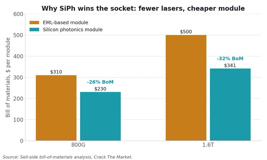
图 1|硅光为何赢得插槽:更少的激光器、更低的模块物料成本。800G 由 EML 方案的 310 美元降至 230 美元(−26%),1.6T 由 500 美元降至 341 美元(−32%)。
The wafer: what sits under the PIC
A SiPh PIC is not built on a plain silicon wafer. It needs a silicon-on-insulator (SOI) wafer with a thick buried oxide so that light stays confined in the top silicon layer. This grade of wafer is called Photonics-SOI, and as Ozeco set out in Soitec: The Photonics Monopoly and PhotonCap covered in The Wafer That Used to Roll Around My Lab Is Now an AI Data Center Bottleneck, it is made almost entirely by one company. Wafer size matters: 200mm lines are the legacy base of the industry, 300mm lines carry 2.25 times the die per wafer and are where every expansion in this piece is going.
The factory: foundry versus IDM, merchant versus captive
A foundry manufactures chips designed by other companies. A fabless company (InnoLight, Credo, Lightmatter, Ayar Labs) designs the PIC and buys wafers from a foundry. An IDM (STMicroelectronics, Intel, Samsung Electronics) designs and manufactures its own chips, and may also sell manufacturing to others. A process design kit (PDK) is the rulebook a foundry hands its customers, and it is the reason switching foundries is slow: a PIC designed for one PDK has to be redesigned for another, and requalified, which takes six to twelve months.
Merchant capacity is sold to any qualified customer. Captive capacity is reserved for one ecosystem, either because the foundry owns the design or because the chip only works inside that foundry’s packaging flow. The distinction is the spine of this piece, because the merchant foundries and the captive one are exposed to different customers, different form factors and different pricing.
The form factors: pluggable, NPO, CPO
Optics reach a switch or a GPU in one of three ways. A pluggable transceiver is a module the size of a USB stick that slots into the front of a switch, today at 800G and 1.6T, tomorrow at 3.2T. Near-packaged optics (NPO) moves the optical engine onto the board next to the switch chip but keeps it removable. Co-packaged optics (CPO) bonds the optical engine onto the same package as the switch or GPU, which saves power and reach but makes the engine part of the chip package rather than a component. The foundry that makes a pluggable PIC sells a wafer to a module maker. The foundry that makes a CPO engine sells a packaging slot to a chip designer. PhotonCap covered the different architectures in DSP, LPO, NPO, CPO
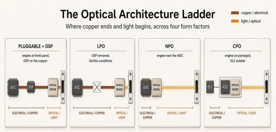
图 2|光互连架构阶梯:可插拔+DSP / LPO / NPO / CPO 四种形态,铜与光的边界逐级前移。
Image Source: DSP, LPO, NPO, CPO
The stack, top to bottom
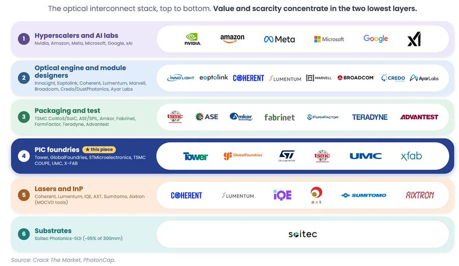
图 3|光互连栈自上而下六层:超大规模客户 → 光引擎与模块 → 封装测试 → PIC 代工 → 激光器与 InP → 衬底。价值与稀缺性集中在最下两层。
Why we are looking at this layer now
Three things changed in 2026 and none of them was about lasers:
Foundries started taking prepayments. Tower booked $290m of customer prepayments in a single quarter to reserve 2027 capacity. Soitec is signing multi-year capacity reservation agreements with eight of its roughly ten major Photonics-SOI customers. STMicroelectronics says a significant number of customers are asking for long-term agreements with cash advances. In semiconductors, customers only pay for capacity that does not yet exist when they believe it will not be there otherwise.
Silicon photonics became the majority platform. SiPh crossed half of AI optics units in 2026 and is headed to between roughly 73% and 84% by 2030, depending on which modulator wins at 400G per lane. Every one of those units needs a PIC, and a PIC needs a fab that can make one.
Every foundry announced a 300mm expansion at once. Tower in Japan, GlobalFoundries in New York and Singapore, STM at Crolles, UMC in Singapore, Samsung Electronics in South Korea. They all land in 2027 and 2028.
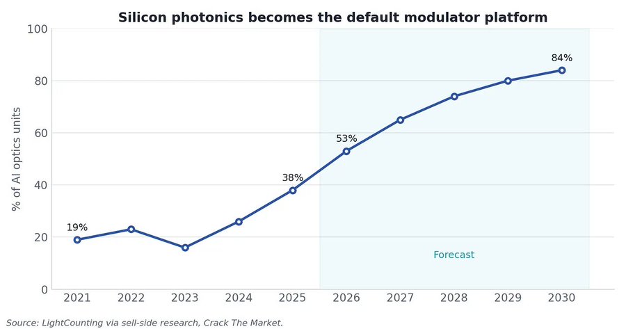
图 4|硅光成为主流调制器平台:占 AI 光器件单元份额 2021 年 19% → 2026 年过半 → 2030 年 84%(LightCounting)。
The layer is not unknown. Tower has tripled, Soitec has tripled, and PhotonCap wrote the first piece on the foundry pricing signal in June. What the layer is, is unmapped. Nobody has written down who can fabricate a PIC today, on which platform, at what wafer size, for which customers, with what capacity, and what sits underneath it. The consequence of a missing map is mispricing: an IDM that is a merchant PIC supplier at Tower’s scale is counted as a chipmaker, a foundry that calls itself the largest pure-play has been overtaken, and a foundry that is functionally captive is modelled as merchant. That is what this piece sets out to fix.
2. The thesis
The optical transition is becoming a consensus. The scarce asset is the capacity to fabricate the PIC, and that capacity sits in five fabs run by four merchant foundries and one quasi-captive one, all of which are expanding at once into 2028.
Five claims we intend to defend, each with a number behind it:
Merchant SiPh is a three-horse race, not a two-horse one. Tower runs at a SiPh run-rate above $680m (Q2 2026) heading to $1bn in Q4. GlobalFoundries guides to more than double its 2025 base of over $200m. STMicroelectronics, absent from every foundry map we have read, is modelled by the sell-side at roughly $800m of SiPh revenue in 2026 and $2bn in 2027. On the headline number STM out-earns both. On a wafer-comparable basis it sits at Tower’s scale and level with GlobalFoundries’ 2028 target. Either way it belongs on the map and is not on it.
The binding constraint is wafer starts today and packaging tomorrow. Tower’s Fab 7 runs above its 85% utilisation model. GlobalFoundries says it is “chasing supply”. STM says capacity is the only constraint. Once 300mm capacity lands in 2027 and 2028 the constraint moves to BiCMOS EICs, InP lasers, and optical wafer test and fibre attach.
CPO does not route through the merchant foundries. TSMC COUPE fabricates for Nvidia, Broadcom, Ayar Labs and Marvell (Celestial), and it only monetises inside TSMC’s own 3DFabric flow: SoIC bonding and optical test for today’s switch engines, CoWoS once optics move beside the GPU for scale-up from 2028. GlobalFoundries, Tower and UMC are betting on pluggables and NPO carrying the volume through 2028. GlobalFoundries itself says CPO is a relatively small contribution by 2028.
2028 will see four merchant 300mm expansions collide. Tower Arai (ready Q4 2027) and its second Japan fab (Q4 2028), GlobalFoundries Malta, STM quadrupling SiPh capacity by 2027, UMC’s Singapore shells, with Samsung’s foundry service arriving from 2027 on top. Demand has to absorb all of them or wafer pricing, which Tower’s CFO names as the single largest sensitivity in its model, gives back the margin it has just taken.
Everything above routes through one substrate supplier. Soitec holds roughly 95% of 300mm Photonics-SOI and sells to GlobalFoundries, TSMC, Tower, STM and imec. Every 300mm expansion in this piece is a Soitec order, and Soitec has just guided Photonics-SOI to 2.5 to 3 times last year’s level. The layer beneath is a tighter monopoly than the layer this piece maps.
What we are not claiming: that the foundry layer captures the most value in the stack (the laser layer’s pricing power is at least as strong), or that today’s contracted revenue survives a 2022-style capex reset intact.
3. The map: who can fabricate a PIC today
Six companies fabricate datacom PICs at production scale. Only three disclose SiPh revenue, and none disclose SiPh wafers per month. The table is what filings, transcripts and disclosed customer relationships support as of September 2026. Blanks are gaps, not zeros.
Table A. Platform and model
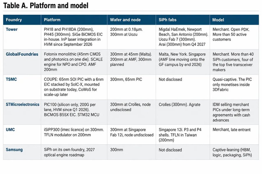
图 5|平台与商业模式(原文 Table A):六家代工厂的工艺平台、晶圆尺寸/节点、产线分布与 merchant/captive 属性。
Table B. Scale, capacity and customers
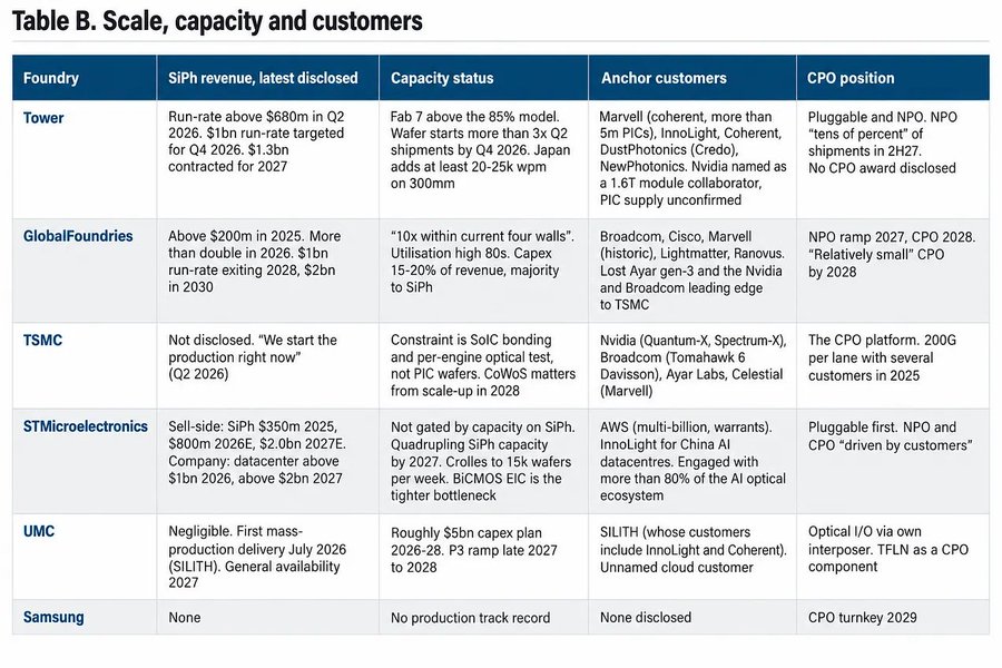
图 6|规模、产能与客户(原文 Table B):各家最新披露的硅光收入、产能状态、锚定客户与 CPO 定位。
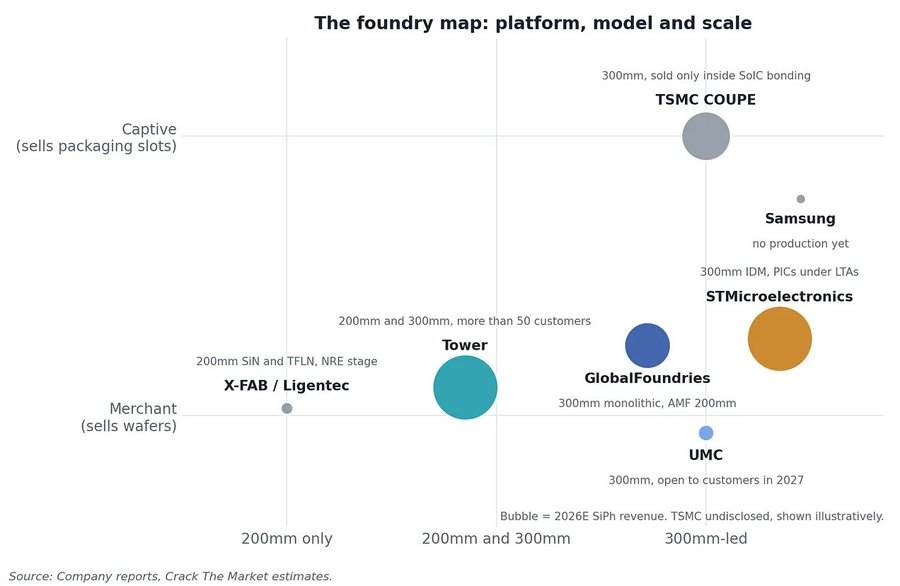
图 7|代工厂地图:横轴为晶圆尺寸(200mm→300mm 为主),纵轴为 merchant(卖晶圆)到 captive(卖封装槽位),气泡大小代表 2026E 硅光收入。
Below this tier sit X-FAB (200mm XPH90 with Ligentec SiN and TFLN, NRE stage, product revenue 2027-28), Silterra (Malaysia, 200mm), SMART Photonics (InP, Netherlands) and Intel (in-house, little merchant traction). Section 9 covers them.
Two things jump out:
First, GlobalFoundries’ “largest pure-play SiPh foundry” claim from the AMF acquisition no longer holds on revenue: Tower’s Q2 2026 run-rate is more than 1.5 times GlobalFoundries’ full-year 2026 guide.
Second, STM does not appear in any sell-side foundry map, and on its headline numbers it out-earns both merchant leaders in 2027.
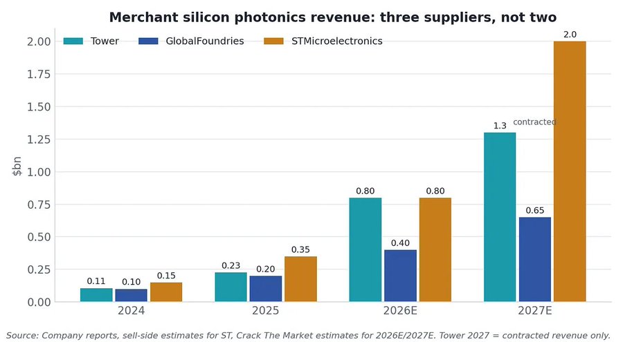
图 8|商用硅光收入是「三家而非两家」:Tower、GlobalFoundries、STMicroelectronics 的收入轨迹对比(2027 年 Tower 为已签约收入)。
4. Tower: the merchant leader, from 200mm PH18 to 300mm Japan
Tower is a merchant foundry, building silicon photonics (SiPh) chips that customers design. Its 200mm PH18 and 300mm PH45 platforms are both in high-volume production for 400G to 1.6T modules. PH18DA bonds indium phosphide (InP) onto the silicon for on-chip lasers and modulators, and NewPhotonics began volume shipments of these photonic ICs (PICs) on 17 September. Tower also makes SiGe drivers and TIAs, the fast analog chips on either side of the optics, in volume at 100G and 200G per lane.
At 100G and 200G per lane the driver and PIC are separate chips, so one foundry for both is mostly a supply convenience. At 400G per lane the driver has to sit on the modulator to cut parasitics, and Tower already offers wafer bonding to stack SiPh and SiGe wafers. Owning both processes and the bond then becomes, in PhotonCap’s view, a performance moat, though no stack customer is named yet.
Growth is moving to 300mm in Japan. By Q4 2027 Arai joins Fab 7 with 300mm SiPh and bonding, and CEO Russell Ellwanger expects “all of the growth” in SiGe and SiPh to be on 300mm from sometime between 2027 and mid-2028. We covered the expansion in The More Silicon Wins, the More InP Sells: Why UMC and Tower Both Expanded 300mm on the Same Day. PH18 to PH45 is a real port: new lithography and etch tools mean waveguides, couplers and doping are re-characterized and the module requalified. We expect most customers to move at the 3.2T, 400G per lane boundary, when they tape out a new PIC anyway. Moving a PH45 design from Fab 7 to Arai is close to a copy.
A bonded laser is patterned by lithography aligned to the waveguides, so it needs no active alignment and can be tested at wafer probe. A bad one cannot be swapped out, though, so laser yield, which is unpublished, multiplies into PIC yield. External CW lasers can be screened and replaced, so switch co-packaged optics (CPO) keeps them outside. We expect the two to coexist by application. Integration wins where an engine needs many lasers at moderate power, in DR8 pluggables and serviceable near-packaged optics (NPO) engines like NewPhotonics’. It also spares module makers a CW laser that has been short all year (see Everyone Saw a Laser Shortage. The Money Went to the Foundries First.). With no 300mm laser flow disclosed, that edge stays tied to 200mm PH18DA for now.
A silicon Mach-Zehnder modulator (MZM) passed 420 Gb/s per lane with Coherent in March. PhotonCap’s read is that in production it carries 400G only in pluggables with a DSP, the digital chip that cleans up the signal, and that is where we expect Tower’s first 400G volume. Above 200 GBd in PAM4 a carrier-depletion MZM runs short of bandwidth, so the link leans on DSP equalization and a high-swing SiGe driver. Linear-drive engines, including linear NPO and CPO, have no DSP, so they turn to PH18DA’s InP modulators, with TFLN, which Tower has in development, later in the decade.
DustPhotonics is covered in A $750M Fabless Chip Company, and the Foundry That Makes the Chips. Nvidia is a named 1.6T module collaborator, but no Tower release we checked says Tower makes its PICs. Nvidia’s switch engines are TSMC COUPE-based CPO for its own switches, while NPO engines like NewPhotonics’ serve other switches, ASICs and operators who want swappable engines, so today the two complement each other. At 400G per lane we expect them to compete for hyperscalers’ scale-out ports, CPO on power and NPO on serviceability (section 6).
SiPh reached a $680m annual run rate in Q2 2026, aiming for $1bn in Q4, and customer advances and deferred revenue rose to about $320m by June from under $30m at end-2025. Company gross margin, which Tower does not split out for SiPh, reached 30% from about 22% a year earlier. Contracts cover about $1.3bn of 2027 SiPh revenue, and Ellwanger said the capacity beyond them is not all booked, “but it’s spoken for”. Q3 results in November, against a $520m guide, are the next check.
5. GlobalFoundries: 300mm monolithic scale, and what it ceded to TSMC
GlobalFoundries builds silicon photonics in Malta on Fotonix, a 300mm process that puts 45nm-class SOI CMOS and photonic devices on one wafer, so the driver chip (EIC) and photonic chip (PIC) can share one flow, though GF also supports a bonded EIC. CEO Tim Breen says 200G per lane is in volume production and 400G has been demonstrated.
PhotonCap thinks the modulator type and the digital logic decide whether 45nm monolithic is good enough for a CPO engine. A silicon Mach-Zehnder modulator (MZM) needs a large swing: GF’s 200G MZM at OFC 2026 takes about 1.8 V·cm (voltage times length to fully switch it), several volts for a few-millimeter arm. That suits a 45nm SOI driver (the OFC paper itself used an off-chip one, as PhotonCap noted in [OFC 2026] Part 1 of 5: 300mm SiPh Foundry: Who Is Actually Ready?), and on the receive side monolithic removes the photodiode-to-TIA bond, where GF has shown a 100 GHz TIA. Micro-rings need less swing but a thermal lock loop per ring, logic that is cheap at an advanced node and costly at 45nm. TSMC’s COUPE hybrid-bonds an advanced-node EIC onto the PIC with little added capacitance (Section 6), erasing most of monolithic’s parasitic advantage. So Fotonix fits MZM pluggables and receivers, and COUPE fits ring-based CPO. The first switch engines went that way: Nvidia’s ring-based engines are built on COUPE (Section 6), and Broadcom’s Tomahawk 6 Davisson puts COUPE-based engines on the package substrate. Even GF’s own ring-based engine, SCALE, puts its EIC on “single-digit advanced nodes”.
SCALE, PhotonCap thinks, aims at a different market. Its 50G and 100G multi-wavelength rings fit scale-up, and GF calls it the first platform ready for the OCI MSA, the open scale-up optics spec. At those lane rates its microbump-class pads, below 45um pitch, are enough. Buyers of custom scale-up engines want a second source, and GF adds a detachable fiber plug and wafer-level optical test. So we see SCALE chasing those engines rather than TSMC’s switch engines.
With no disclosed in-house InP laser growth, GF relies on SMART Photonics laser dies flip-chipped into etched silicon pockets, a service generally available in 2H27. We read this as a process choice with a time cost. Flip-chip lets GF attach pretested lasers and the customer choose the InP vendor, at the cost of sub-micron alignment on every die. In CPO that matters less, since leading engines use external lasers, field-replaceable on Davisson. In pluggables Tower and NewPhotonics already ship laser-integrated PICs in volume (Section 4), about a year ahead of the SMART service.
For 400G per lane GF’s March blog names Pockels (field-driven) materials: thin-film lithium niobate (TFLN), barium titanate (BTO) and electro-optic polymers. We think TFLN reaches a 400G product first, even though BTO is already offered for today’s pluggables. Lithium niobate has the longest telecom reliability record, and AMF brought TFLN and polymer 400G modulator work into GF, per Gazettabyte (trade press), so we expect that product from AMF’s Singapore line.
Beyond switch CPO on the substrate, CoWoS-class integration beside a GPU or XPU arrives with scale-up optics, due on Nvidia’s NVLink in 2028 (Section 6). Breen put NPO in 2027 and CPO in 2028, which we read as matching that wave more than a GF-specific delay.
GF guides 2026 SiPh revenue to “more than double”, mostly from pluggables today, and a July letter of intent points to a $300m Commerce award for SiPh wafers, materials and packaging. Ozeco reads GF as a pluggable foundry with a government-funded materials roadmap, a business that lasts as long as pluggables do.
6. TSMC COUPE: quasi-captive through SoIC bonding
Public disclosures name one maker for the switch CPO engines shipping in 2026: TSMC. Its 2025 annual report says COUPE reached 200 Gbps “with several customers in 2025” and targets CPO volume production in 2026. COUPE uses SoIC-X, TSMC’s solder-free 3D stacking, to bond the electrical die (EIC) face-down onto the photonic die (PIC). Its modulator is a 200G micro-ring, a tiny resonant loop tuned to one wavelength. Nvidia’s Quantum-X Photonics and Broadcom’s Tomahawk 6 Davisson both use COUPE engines, with external lasers.
CoWoS places chips side by side on a silicon interposer, as GPUs sit next to HBM. TSMC’s 2024 plan put COUPE into CoWoS in 2026; by April 2026 the milestone read COUPE on substrate, with CoWoS-based CPO for ultra-high-end switches still in development. Today’s switches don’t need the interposer, since Broadcom uses substrate-level packaging and Nvidia solders its Spectrum-X engines onto the module substrate. CoWoS pays off when the engine sits beside a GPU or XPU for scale-up optics, the links inside one accelerator system; Nvidia plans CPO on NVLink ports in 2028. PhotonCap separated those two races in TSMC Is Ahead in CPO. Samsung Is Putting a Third Chip Next to HBM. The CoWoS queue belongs to a later generation, XPU scale-up and TSMC’s ultra-high-end switch package; today’s switch engines wait on SoIC bonding.
We see the PIC wafer as the least scarce input, since photonics runs on mature nodes with few mask layers. Downstream, a hybrid bond at a few microns of pitch cannot be reworked, so both dies are tested before bonding and each engine is probed optically, ring by ring. Engine yield multiplies EIC, PIC, bond and coupling yields, and only the first two are ordinary wafer-fab problems. TSMC’s K.C. Hsu likewise put the bigger challenge in lasers, fibers, connectors and testing. The bond stays in TSMC’s fab; assembly and test can go outside, as SPIL does for Nvidia. That split is what we mean by quasi-captive.
Pre-bond probing, done on one face of the wafer with electrical needles and optical fibers, is where we think most test revenue sits today. FormFactor expects 2026 CPO revenue to “significantly exceed the $20 million level”, per an Investing.com transcript of its Q2 call. Advantest is developing high-volume SiPh test with OpenLight. In a COUPE-style stack the electrical contacts end up on one face and the surface-coupled optical ports on the other, so confirming an engine works before it reaches a costly switch package means probing both faces. Teradyne introduced Photon 100 at OFC in March 2026, a year after a double-sided cell with ficonTEC for hybrid-bonded wafers, and PhotonCap’s read is that double-sided probing becomes a required step once engines ship in volume. SoIC bonding and engine-level optical test share third place in our chokepoint ranking for CPO because a bonded engine cannot be reworked and a bad one must be caught before it reaches the switch package.
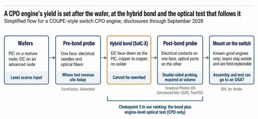
图 9|COUPE 式 CPO 引擎的良率在晶圆之后被决定:预键合探测 → SoIC-X 混合键合(不可返工)→ 键合后双面探测 → 上交换机。键合与引擎级光学测试并列我们的第三瓶颈。
TSMC says COUPE supports both grating couplers (light exits the chip surface) and edge couplers (light exits the die’s side), and can now test edge couplers at wafer level. In PhotonCap’s experience, edge couplers win on loss and bandwidth but were hard to test, since the facet exists only after dicing. With that fixed we read the two as splitting by application, edge coupling for TSMC’s next generation and gratings for Nvidia’s surface-normal engines.
Nvidia’s Quantum-X engines sit in sealed, socketed subassemblies, and in Nvidia’s 2025 launch description the lasers are the field-replaceable part. NPO, near-packaged optics, puts a swappable engine beside the ASIC instead, and NewPhotonics began volume shipments of laser-integrated Tower PICs for it on 17 September, with 6.4T NPO chipsets slated for the first half of 2027. At today’s 200G per lane we see the two as complementary: Nvidia’s CPO is tied to its own switches, while NPO serves other switches, custom ASICs and operators who want swappable engines. At 400G per lane we expect them to compete for scale-out ports, the switch network that links racks, CPO on power and NPO on serviceability. On pluggables TSMC is the least proven answer: the 2024 plan to qualify COUPE for pluggables in 2025 has produced no volume product, and nothing public shows TSMC selling bare SiPh wafers to module makers.
The money sits inside SoIC and packaging revenue, with no separate SiPh line. TSMC’s $60-64bn capex guide puts 10-20% in a bucket for “advanced packaging, testing, mask making, and others”.
7. STMicroelectronics: the merchant PIC supplier the maps leave out
STM is not in any foundry map we have read, and on its headline numbers it out-earns both merchant leaders in 2027. On a wafer basis it is a merchant PIC supplier at Tower’s scale. Ozeco covered the company in STMicroelectronics: Photonics, Satellites and Silicon Carbide and the datacenter numbers have moved twice since.
The numbers. Datacenter revenue was raised on 2 June 2026 to roughly $1bn for 2026 and roughly $2bn for 2027, from “nicely above $500m” and “well above $1bn” only months earlier. The CFO at a September conference put roughly 80% of 2027 datacenter revenue in the MDRF segment, which is the connectivity flow (SiPh PIC, BiCMOS EIC, STM32 MCU), and 20% in power and thermal. Optical was roughly $0.3bn in 2025 at above 40% gross margin.
Sell-side models put SiPh alone at $150m in 2024, $350m in 2025, $800m in 2026, $2.0bn in 2027 and $2.5bn in 2028, then flattening towards $3.5bn by 2030.
Orders above $1bn for 2026 and above $2bn for 2027 were secured before the June raise. Q2 book-to-bill was “significantly above 2” in Comms Equipment & Computer Peripherals, more than half of Q2 bookings were for 2027, and the backlog covers 4.5 to 5 quarters.
Comms Equipment & Computer Peripherals grew 50% year on year in Q2 and is guided to roughly 60% in Q3 and 90% in Q4.
The platform. PIC100 is a silicon-only 300mm platform at Crolles, 200G per lane, in high-volume manufacturing since Q1 2026 for 800G and 1.6T. STM has been investing in SiPh at Crolles since 2014 and is the only large European IDM with a 300mm SiPh line at scale. The EIC is STM’s own BiCMOS B55X, also at Crolles, where STM already holds more than 30% EIC share. The control-plane MCU is the STM32, where STM claims an oversized share in 800G and 1.6T. Three chips in every pluggable from one fab is impressive, and it is why the AWS agreement (multi-year, multi-billion, announced 19 February 2026, with warrants on up to 24.8m shares at $28.38 vesting on purchase volumes) covered PICs, EICs, MCUs and power together. The node is undisclosed in every document. Whether PIC100 sits on Soitec Photonics-SOI is not stated by STM, but STM is on Soitec’s customer list.
Capacity. “We are not right now gated by capacity expansion” on SiPh. SiPh capex is fungible with MCU on 300mm, “an increase in slicing” rather than a new shell, which is the structural advantage of running photonics inside a large 300mm logic fab.
Crolles will reach 15,000 wafers per week and go above it. Crolles plus Agrate can reach 20,000 300mm wafers per week at full build-out before 2028.
STM plans to quadruple SiPh capacity by 2027. 2026 net capex is at the high end of $2.0-2.2bn, explicitly rebalanced towards optical interconnect.
The tighter bottleneck is BiCMOS, with 12-18 month equipment lead times. 300mm lets STM add SiPh capacity without customer re-qualification. Management flags a pocket of OSAT constraint.
Contracting. A “significant number” of customers are asking for long-term agreements “locking capacity, volumes, pricing and cash advance for many”, running one to three years. This is the same prepayment mechanism PhotonCap identified at Tower, appearing at an IDM that no one classifies as a foundry.
Concentration. STM says datacenter revenue is “pretty consistent with market share distribution between hyperscalers”. Sell-side work puts AWS at no more than roughly 30% of datacenter revenue in 2027 and has STM engaged with more than 80% of the AI optical ecosystem. STM also supplies Chinese AI datacentres through InnoLight and other module makers. The 30% figure is a 2027 target, not today’s mix.
What is missing. No laser sourcing comment anywhere, which implies STM ships un-lasered PICs and the module maker attaches the CW laser. No CPO revenue or timing: “we have all the ingredients, including packaging, this will be driven by our customers.” No node. And one sell-side model already flags a moderation in photonics growth beyond 2027 that AI power has to offset. STM’s SiPh number is an IDM number, PIC plus EIC plus MCU at IDM pricing, and it has to be put on a wafer-revenue basis before it can be compared with Tower and GlobalFoundries. That is what we do later in the piece, in Section 12.
8. UMC, Samsung, Intel and the entrants
At UMC, silicon photonics starts with iSiPP300, a 300mm process licensed from imec in December 2025 and built around ring modulators and filters (small circular waveguides that resonate at one channel’s wavelength), GeSi electro-absorption modulators and 3D packaging modules. The first volume product on the Singapore 300mm line is a customer design, and the release doesn’t tie it to the imec process. On 14 July UMC and SILITH announced the first mass-production delivery of 300mm PICs for SILITH’s 1.6T platform at 200G per lane, qualified by a leading cloud infrastructure customer, and the two are now building a 400G-per-lane platform on silicon Mach-Zehnder modulators (MZMs).
Alongside it, UMC has thin-film lithium niobate (TFLN), a crystal film whose refractive index shifts directly with voltage, which gives high bandwidth at low drive voltage. HyperLight’s TFLN chiplet platform is qualified in volume at Wavetek, a UMC subsidiary, on 150mm wafers, with 200mm capability added. On the Q2 call, per Investing.com’s transcript, CEO Jason Wang said UMC is working on 400G per lane for a customer’s 3.2T design on TFLN, which could be combined with UMC’s silicon PIC through its advanced packaging.
PhotonCap expects silicon MZMs and TFLN to coexist at 400G per lane for a while. Silicon MZMs should keep the volume DSP pluggables on cost and CMOS manufacturability, as the Tower and Coherent 420 Gb/s demo suggests (Section 4), while TFLN gets in first as a chiplet next to the silicon PIC where low drive voltage and high bandwidth matter most.
From 2027, when its filing says the platform opens for general customer use, UMC joins GF, Tower and ST as a 300mm SiPh line for any customer’s designs, so wafer size alone doesn’t differentiate it. What it has on top is the combination of a 300mm SiPh line, a separate TFLN manufacturing line (on 150mm and 200mm wafers, not 300mm) and in-house packaging inside one group, which no other merchant foundry here offers today. Ozeco’s read is that UMC becomes the first real alternative source of 300mm PIC wafers once its P4 cleanroom in Singapore ramps in late 2027 to early 2028, and the sign to watch is a second named SiPh customer beyond SILITH before then. UMC raised 2026 capex from $1.5bn to $2.0bn in July with no SiPh split. SiPh wafer capacity and revenue are undisclosed, and UMC guides its Q3 dollar ASP to “remain firm”.
Samsung’s 300mm platform, per SemiVision Research’s summary of its OFC 2026 paper (secondary), uses a 305nm top silicon layer, a 400nm SiN layer, PN-doped modulators and germanium photodiodes. PhotonCap doesn’t see 305nm as a unique porting barrier, but it does mean more redesign for thickness-sensitive devices such as rings and grating couplers. The Elec reported in September that in-house PIC wafer test was still under way, with foundry service from 2027.
Intel has the longest SiPh volume record here, from a platform that integrates lasers on the die at wafer scale: over 8 million PICs and over 32 million on-chip lasers, mostly in its own pluggables.
In China, CanSemi has a 300mm 90nm SiPh platform at trial production and has not named a datacom module customer.
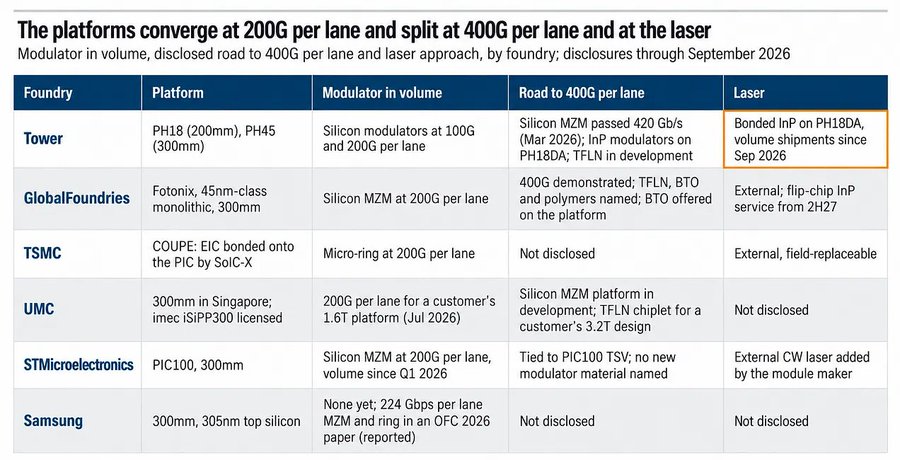
图 10|各厂在 200G/lane 汇聚,在 400G/lane 与激光方案上分叉:调制器在产状态、400G 路线与激光器策略对照。
9. The European specialty layer
Europe has one volume SiPh fab (STM’s Crolles), one volume substrate supplier (Soitec), and a set of 200mm specialty platforms that serve a different market: low-loss silicon nitride, heterogeneous integration, InP, high-mix. Though Europe has no pluggable PIC foundry today. This is consistent with Ozeco’s framing in The European Photonics Supercycle and The US Photonics Supercycle: Europe owns the tools and substrates upstream, America owns the lasers, the silicon and the systems.
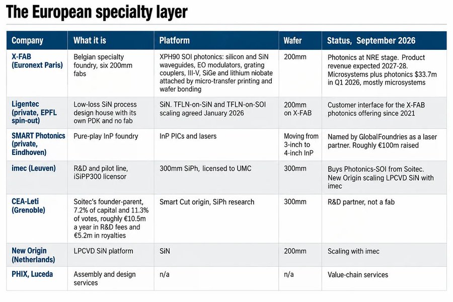
图 11|欧洲特色工艺层:X-FAB、Ligentec、SMART Photonics、imec、CEA-Leti、New Origin、PHIX/Luceda 的平台与 2026 年 9 月状态。
Three observations on Europe’s positioning:
X-FAB is the only listed European specialty name with a credible volume path, and its photonics is optionality for 2027-28 rather than pricing power today. The share price moved on the silicon carbide and SiPh narratives before the revenue.
SiN and TFLN are the next curve, not the current one. LightCounting has TFLN barely visible in 2026 and appearing from 2027 in DWDM. That is where Ligentec with X-FAB and UMC’s TFLN line compete, not where Tower and GlobalFoundries earn today.
The European layer’s real weight is upstream. Soitec substrates and Aixtron epitaxy tools, which the next section covers, and STM, which is the only European name in the volume tier.
10. The layer beneath: substrates, InP and epitaxy
A foundry’s capacity build is only realised on top of its materials supply, and the materials layer is more concentrated than the foundry layer it feeds.
Soitec: the wafer under every 300mm expansion
Soitec does not make chips. It makes the engineered substrates that other people build chips on, and in photonics that makes it the single point every foundry in this piece passes through.
Smart Cut is roughly the entire SOI market. Soitec holds roughly 80% of SOI overall and roughly 95% of 300mm Photonics-SOI, on which the industry is standardising.
Every major SiPh foundry, GlobalFoundries, TSMC, Tower, STM and imec, buys Photonics-SOI from Soitec. The company now talks about “around ten major Photonics-SOI customers”, up from the five it referred to earlier this year.
Photonics-SOI was slightly above $100m in FY26 (March 2026). On 2 September 2026 Soitec raised the FY27 Photonics-SOI outlook to 2.5 to 3 times the FY26 level, so $250-300m, with Q2 FY27 at roughly three times last year’s quarter (about $75m) and the first half at roughly 2.3 times. Group Q2 revenue growth was raised to around 50% from “more than 30%”. Soitec expects multi-year capacity reservation agreements to be in place with eight of its roughly ten major Photonics-SOI customers within weeks, on top of the prepaid reservations already in the commitment book (up to €1.1bn of future sales at 31 March 2026).
The 300mm Photonics-SOI line in Singapore qualified for high-volume manufacturing six months early. As of the FY26 results management said no expansion was needed and fab loading was around 50% against the 60-70% needed for leverage. The September update did not change that, which means the 2027-28 foundry ramps are being absorbed by existing Soitec capacity for now.
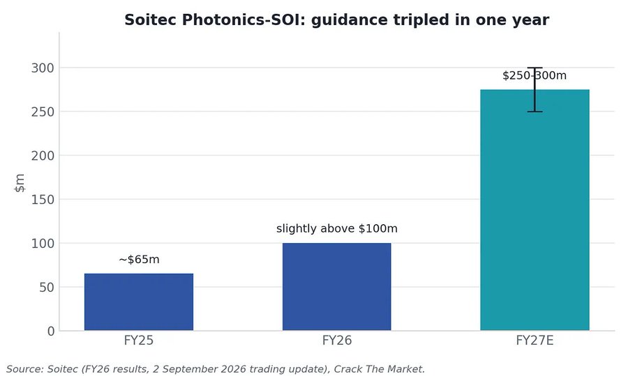
图 12|Soitec Photonics-SOI 指引一年翻几倍:FY25 约 6,500 万美元 → FY26 略超 1 亿美元 → FY27E 2.5–3 亿美元。
In Soitec: The Photonics Monopoly Ozeco built the TAM on $1,300 per 8-inch-equivalent wafer held flat and 8-inch-equivalent Photonics-SOI wafers rising from 65k in 2025 to 406k in 2030, a 44% CAGR, for roughly $528m of datacenter Photonics-SOI revenue by 2030. The September guidance says wafer volumes roughly triple in a single year. At that pace the 2030 endpoint of the framework arrives in 2028, which is the same year the four foundry expansions land. The two series are consistent, and both say the substrate order book leads the fab order book by about a year.
Second-source risk is the one thing to keep watching. Shin-Etsu (licensee since 1997, shareholder), Siltronic (licensee 2004) and GlobalWafers (licence terminated 2025, shipping 300mm SOI, stated intent to serve photonics) are the candidates. Ozeco’s model drifts Soitec’s share from 95% to 80% by 2030 with six to twelve month qualification cycles. Lithium-niobate-on-insulator for beyond-1.6T modulation is in development at Soitec, which is the bridge to the TFLN layer.
InP: the laser’s bottleneck, and now the foundry’s
200G per lane EML supply and most of the CW laser and photodetector chain run on InP substrates and epitaxy. In Coherent & Lumentum Ozeco argued that in this layer capacity is revenue, and the numbers since have followed the capacity ramps exactly.
Coherent grew InP output 80% year on year in the June quarter, doubles capacity by the end of the September quarter and again by end 2027, almost entirely on 6-inch, which gives more than four times the die per wafer at roughly half the cost per device. Four InP fabs: Fremont, Sherman (first 6-inch, ultra-high-power CPO lasers), Järfälla and Zurich.
Lumentum’s two Japanese 4-inch fabs are fully allocated, capacity is up roughly 40% in three quarters, Greensboro is native 6-inch with first revenue early 2028, and the company holds more than 50% EML share at 100G and 200G.
Nvidia put $2bn of equity into each in March 2026 with multi-year purchase commitments and capacity rights. Lumentum’s CEO said Nvidia could take all remaining capacity.
Substrates: Sumitomo Electric (targets more than double capacity 2023-28), AXT (not yet on 6-inch, China-domiciled manufacturing), JX, Freiberger. Epiwafers: IQE, now under a multi-year minimum-commitment agreement with Tower, and VPEC.
Industry consensus has light sources tight through 2027 and balanced in 2H28.
The point for the foundry map: Tower’s integrated-InP strategy, now in high-volume production with NewPhotonics, pulls the laser bottleneck inside the foundry gate, while GlobalFoundries, STM and UMC leave it with the module maker.
Aixtron: the tool under the epi
Aixtron holds roughly 90% of MOCVD for optoelectronic epitaxy and is the only commercial platform for InP CW and EML layers, with an 18-24 month switching cost. Epitaxy is 40-60% of laser wafer cost. After the Nvidia deals management guided 60-120 InP tools a year at €3-3.5m each, €180-420m against a roughly €100m 2025 base. The G10 tool on 6-inch raises output per run 1.5-2.5 times plus a 33% yield gain, which means fewer units for the same capacity, and that is the risk in the tool count.
Chokepoint ranking
Ranked by substitutability and lead time:
Soitec Photonics-SOI. No qualified 300mm second source, six to twelve month qualification, order book leading the fabs by a year.
InP epi and 6-inch substrates. Tight to 2027, balanced in 2H28, and now being locked by foundries as well as laser makers.
SoIC hybrid bonding and engine-level optical test (CPO only). Cannot be reworked, single supplier, and the step that gates switch engines today.
Merchant SiPh wafer starts. Tight today, four expansions landing 2027-28.
MOCVD tools. Constrained by unit count, not by share, and eased by the 6-inch productivity gain.
11. Who designs into which fab
The foundry map only matters if we can say who is designing into each fab. This is the table that does not exist anywhere else, and it is assembled from disclosures where they exist and attributions where they do not. Each row carries its evidence grade: D disclosed by one of the parties, A attributed by industry research or trade press, I our inference.
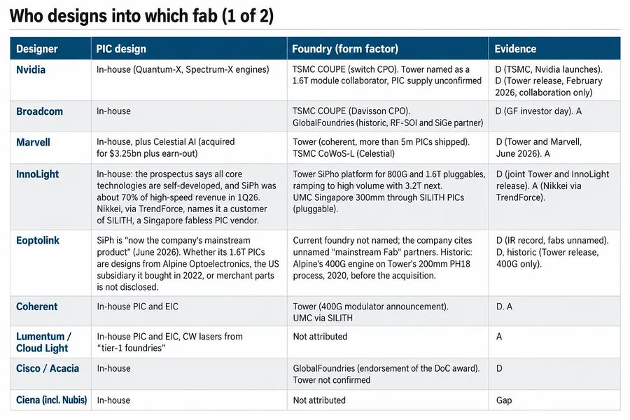
图 13|谁在设计进哪家 fab(1/2):设计方、PIC 设计归属、代工厂与形态、证据等级(D 披露 / A 转述 / I 推断)。
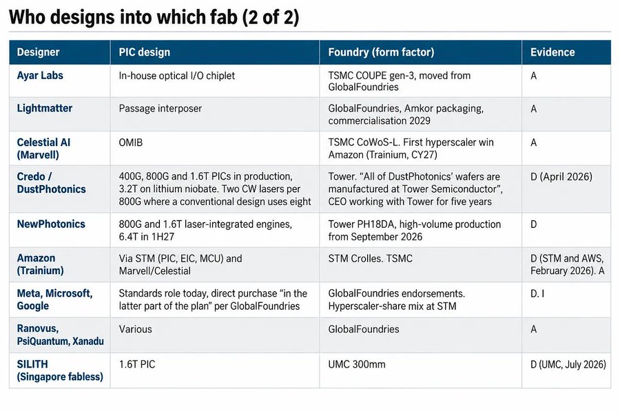
图 14|谁在设计进哪家 fab(2/2)。
Three observations:
Tower’s customer list is the broadest and the best confirmed, and it got two more confirmed names in the last five months (DustPhotonics through PhotonCap’s April piece, NewPhotonics through Tower’s own release). That is why its contracted revenue is the cleanest signal in the layer.
The CPO customers are all at TSMC, and the ones that started at GlobalFoundries (Ayar Labs, and the Nvidia and Broadcom leading edge) left. GlobalFoundries’ customer list is now a pluggable and quantum list.
Credo matters more than its size suggests. In Credo: When a De-Rating Is a Gift Ozeco set out the FY27 optical target above $600m across DSPs, PICs and ZeroFlap transceivers, with ZeroFlap at 100k units a month exiting the year and two merchant 1.6T PIC design wins for FY28. All of that PIC volume now lands on Tower’s 200mm lines, which is a second reason to read Tower’s “spoken for” capacity as real.
Only silicon photonics modules need a SiPh wafer; EML modules (laser and modulator on one indium phosphide chip) and VCSEL modules do not. LightCounting’s forecast has AI optical modules growing from about 36m units in 2025 to about 130m in 2030, with the SiPh share rising from 38% to 84%. That takes SiPh modules from about 14m to about 110m, twice the market’s growth.
The reason is mostly the laser. An EML-based 1.6T DR8 (eight parallel 200G fiber lanes each way) needs eight 200G EMLs, while a SiPh DR8 can run off as few as two high-power CW (always-on) lasers, each shared by four lanes. Some designs use four. In PhotonCap’s view, the 200G EML has been the tightest part of the optics supply chain through the 1.6T ramp, on yield and capacity. The saving holds only in parallel designs like DR8. A 2xFR4 module, four wavelengths on each of two fibers, still needs one laser per wavelength, and there EML holds on.
PhotonCap reads 84% as an upper bound that needs silicon to hold the next lane speed. The public series is lower: CIC, in InnoLight’s prospectus, ends at 73% of datacom optical revenue in 2030. Tower and Coherent have run 400G per lane through a silicon modulator, but Coherent also showed a 400G differential EML and InnoLight a 200G per lane TFLN modulator, a candidate for the next speed. If 400G per lane goes to EML, unit share likely stalls near 73% or below. TFLN bonded onto a silicon PIC still starts on a SiPh wafer, though.
PICs per module and good die per wafer are not disclosed, so as an explicit assumption we use two PICs per 1.6T module (transmit and receive) and about 1,000 known-good dies per 300mm wafer, as section 12 does. Then 110m modules in 2030 need about 220k wafers a year, roughly 18k wafers per month (wpm). One die per module, as in some 1.6T designs, halves that; 500 good dies per wafer, plausible for a larger die, doubles it to about 37k wpm. These two inputs decide whether 2027-28 capacity looks tight or oversupplied; section 12 makes that comparison.
CIC puts InnoLight at about a fifth of the 2025 optical interconnect market, with an unnamed 14% player that matches Eoptolink by our reading. Both are Chinese, yet every PIC foundry named for them is outside China. If a US rule ever targets suppliers by nationality, module share would shift to non-Chinese makers, and the PIC wafer would move only if those makers use a different foundry.
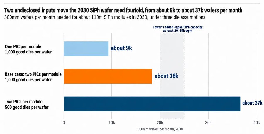
图 15|两个未披露输入让 2030 年硅光晶圆需求放大四倍:约 9k → 约 37k wpm(每模块 PIC 颗数 × 每片良品 die 数)。
12. Capacity arithmetic 2026-2028
No foundry discloses SiPh wafers per month, so the arithmetic has to be done in revenue run-rates and the few physical numbers that exist. Treat the numbers as orders of magnitude.
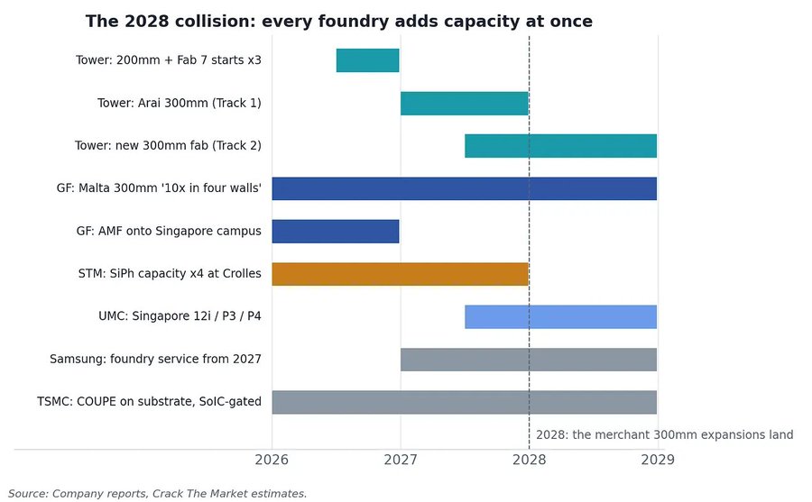
图 16|2028 年碰撞:所有代工厂同时加产能,四家商用 300mm 扩产在 2027–2028 集中落地。
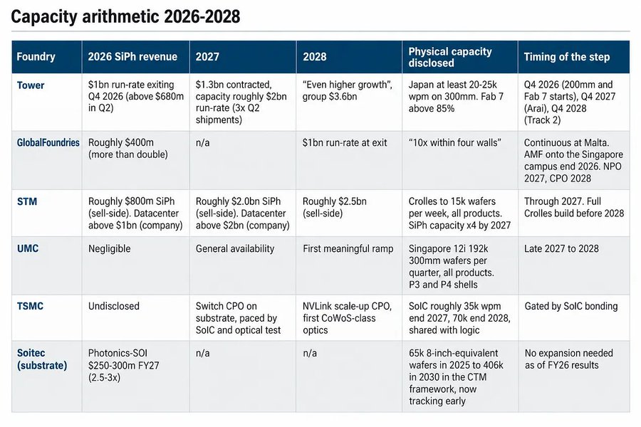
图 17|2026–2028 产能算术:各厂硅光收入、已披露物理产能与上量时点。
Putting STM on a wafer basis. STM’s $2bn of 2027 SiPh revenue in sell-side models is an IDM number: PIC plus BiCMOS EIC plus MCU at IDM pricing. Two chips of the three are silicon photonics, and a merchant foundry would sell only the PIC wafer. Using the module bill-of-materials split (two PICs at roughly $70 in a 1.6T module against a $341 total, and the EIC and MCU at a similar combined value) and applying a foundry wafer margin rather than an IDM chip margin, roughly 40-50% of ST’s SiPh line is PIC value, and roughly 60-70% of that PIC value is what a foundry would book. On that basis STM’s 2027 SiPh revenue is roughly $0.6-0.8bn on a Tower-comparable footing, which puts it level with GlobalFoundries’ 2028 exit run-rate but behind Tower’s 2027 contract book. The headline claim in section 2 survives in the softer form: STM is the third merchant supplier at Tower’s scale, not a hidden number one. That is still a claim no map makes.
The sum. Merchant SiPh revenue on that comparable basis (Tower, GlobalFoundries, STM wafer-equivalent, UMC) runs from roughly $1.5bn in 2026 to roughly $2.8bn in 2027, against a SiPh wafer SAM that GlobalFoundries’ own slide puts at roughly $0.7bn in 2026 rising to roughly $6.5bn by 2032. The 2026 numbers do not reconcile: the merchant tier is already booking about twice the wafer SAM the industry slide shows for the year. Either the SAM slide is stale (it predates the Tower and STM raises) or it counts only the PIC die at a lower price point. Both are plausible and neither changes the conclusion that the 2028 capacity is priced for a demand curve that must keep steepening.
The physical cross-check. Tower’s Japan minimum of 20-25k wpm on 300mm is equivalent to 45-56k 200mm wafers a month on the 2.25x conversion. Soitec’s 2025 base of roughly 65k 8-inch-equivalent Photonics-SOI wafers a year, about 5.4k a month across all customers, says the whole industry ran on a small fraction of what Tower alone plans to add. The September guidance closes part of that gap: Soitec’s FY27 volumes roughly triple, so the run-rate is heading towards 15-20k 8-inch-equivalent wafers a month by early 2027, and at the same growth rate reaches the equivalent of the Japan programme alone by 2028. What the two series say together is that Tower’s Japan capacity is not all SiPh in its first two years, and that Soitec’s “no expansion needed” line will be tested by the end of 2027.
The demand-side cross-check. Section 11 does the arithmetic: about 110m SiPh modules in 2030, two PICs per module and about 1,000 good dies per 300mm wafer come to roughly 18k wpm industry-wide, in a range of 9-37k depending on those two inputs. On the base case, Tower’s Japan minimum alone exceeds the whole industry’s 2030 wafer need. Add GlobalFoundries, STM and UMC, and the risk in 2028 is overcapacity rather than shortage, unless PIC counts per module or die sizes rise at 3.2T.
13. Merchant versus captive: where the value lands
The layer splits by form factor, not by technology. Pluggables are a merchant market with three suppliers taking prepayments. CPO is a captive market with one supplier allocating packaging slots. NPO is the contested middle.
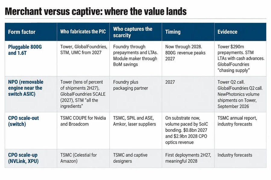
图 18|商用 vs 自用:按形态拆解——谁制造 PIC、谁捕获稀缺性、时点与证据。
The mechanism. PhotonCap’s June framing stands: pricing power belongs to the layer where customers put down prepayments, and in 2026 that is the merchant foundry and the substrate, not the laser. What this piece adds is that the mechanism has a shelf life set by two dates: the 2027-28 arrival of four 300mm expansions, and the point at which CPO volume moves the optical engine from a merchant wafer sold to a module maker into a TSMC 3DFabric slot sold to a switch vendor. GlobalFoundries’ own numbers say pluggables carry it to the $1bn run-rate and CPO is small until then. Tower’s say all 300mm growth after mid-2028 is SiPh. Both are betting that pluggables and NPO outlast the merchant capacity wave.
Value capture by layer, 2026-28. Highest and most durable: Soitec, single-source substrate, prepaid reservations with eight of ten major customers, no expansion needed. High but time-limited: Tower (contracted 2027, prepaid, 67% incremental gross margin) and STM (LTAs, accretive margin, but AWS concentration and a post-2027 flattening in the models). Medium: GlobalFoundries (scale and government co-funding, but mobile drag and lost CPO customers). Optionality only: UMC, X-FAB, Samsung. Indirect: TSMC, whose photonics value shows up in SoIC today and CoWoS later, and ASE and Amkor, whose value rises with CPO. The laser layer sits alongside rather than inside this map and is at least as constrained.
14. Where the thesis breaks
Wafer pricing in 2028. Tower’s CFO: the selling price per wafer is the largest variable in the model and “the selling price is just 100% reflection over the margin”. Four 300mm expansions and a share-hungry UMC land in 2027-28. If demand does not keep steepening, the eight points of gross margin Tower added in a year (30% in Q2 2026 against about 22% a year earlier) come back out.
The 200mm to 300mm requalification. Tower’s customer base was built on PH18 on 200mm. The growth is on PH45 and Arai on 300mm. Every PDK change is a redesign opportunity for the customer to dual-source at GlobalFoundries, STM or UMC. STM says 300mm lets it add capacity without requalification. Tower’s transition is the reverse case.
CPO goes captive faster than pluggables grow. If Rubin Ultra and Tomahawk 6 pull scale-out optics into COUPE engines faster than expected, and the 400G per lane contest between CPO and NPO (section 6) goes to CPO, the merchant tier’s 2028 capacity is built for a market that moved. Industry forecasts have two-thirds of 3.2T ports on CPO by 2030.
The contract book is thinner than it looks. Tower’s $1.3bn is contracted. The other third of 2027 capacity is “spoken for”. GlobalFoundries names no SiPh customer directly. STM’s LTAs are volumes and pricing, and hyperscalers have cancelled optics orders before (2022-23). A capex reset turns prepaid capacity into overcapacity, and Tower’s prepayments cushion it least where the capacity is newest.
Soitec risks losing the monopoly earlier. GlobalWafers is shipping 300mm SOI and wants photonics. A six to twelve month qualification at any of the four merchant foundries during a capacity build is exactly when a second source gets qualified. Ozeco’s model drifts share to 80% by 2030. The risk is that it happens by 2028.
The InP constraint does not ease. If 6-inch InP at Coherent and Greensboro slips, the CW laser supply that SiPh pluggables depend on stays rationed by Nvidia’s capacity rights, and merchant foundry wafers ship without light sources. Tower’s IQE agreement and its in-house laser integration are the only foundry-level hedges in the map.
TFLN and SiN arrive early. LightCounting has TFLN barely visible in 2026 and appearing in 2027 DWDM. UMC has a TFLN modulator in production and a hybrid PIC in risk production Q2 2027. GlobalFoundries’ government money funds BTO and TFLN modulators. If 400G per lane needs non-silicon modulators, the platform advantage shifts to whoever integrates them first, and the 200mm specialty fabs re-enter the volume story.
Israel concentration. Tower’s SiPh base is Migdal HaEmek until Japan scales, and management cites geopolitical neutrality as a reason for Japan.
Our own measurement risk. The revenue series are not like-for-like until STM is put on a wafer basis, and the Soitec wafer count against Tower’s Japan capacity only reconciles with the September guidance. Publishing before both are pinned down would repeat the sell-side’s error of counting the layer without measuring it.
15. Names by layer
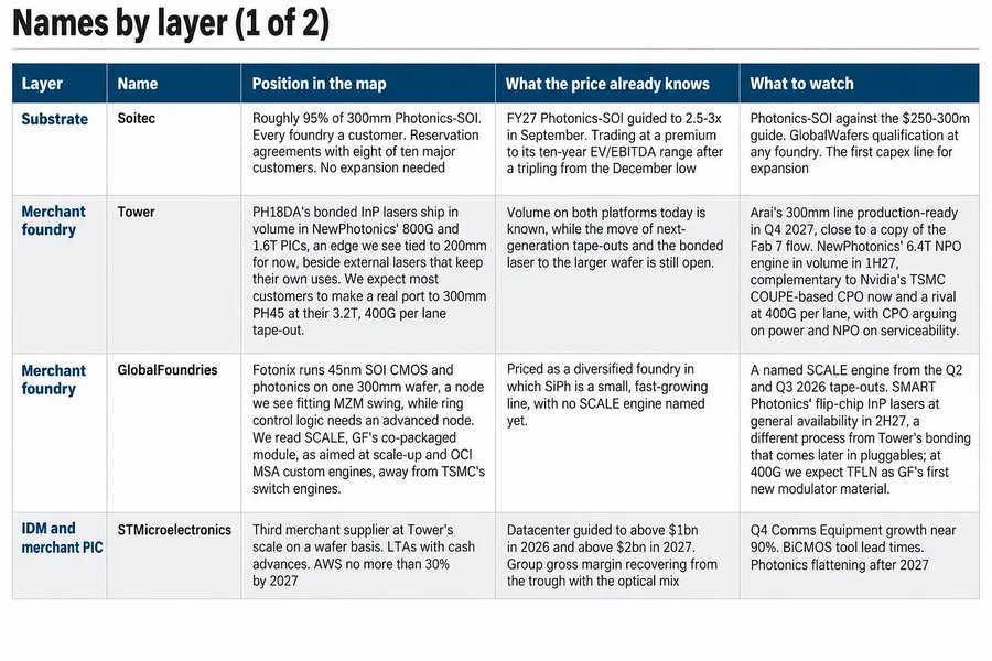
图 19|按层列名(1/2):各层公司在图中的位置、股价已反映的内容与需要观察的信号。
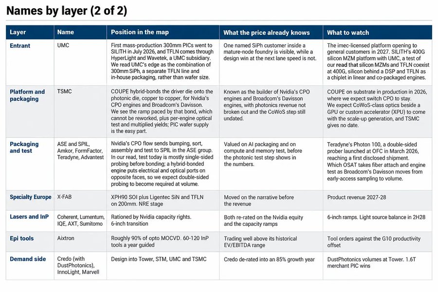
图 20|按层列名(2/2)。
Scenario mapping, extending PhotonCap’s June table:
The base case (demand overhang through 2027) favours Soitec, Tower, STM and GlobalFoundries in that order of signal quality.
CPO acceleration favours TSMC, ASE and SPIL, Amkor and the test names, and is a relative headwind for Tower and GlobalFoundries.
A capex reset is cushioned by contracted revenue at Tower and STM and hurts UMC, X-FAB and Samsung most, with Soitec’s 50% loading the least exposed to overbuild.
16. Conclusion
The optical transition is becoming consensus, and the market has started to price the lasers. What it hasn’t fully mapped yet is the layer that turns those lasers into links.
Today, only six companies can fabricate a datacom PIC at scale. Three are already taking prepayments. One sells only through its own bonding line. All six are building 300mm capacity, and most of that capacity lands within the same eighteen-month window.
And underneath every one of those fabs sits the same substrate supplier.
In the base case, the merchant foundries and Soitec capture the scarcity through 2027. From 2028, the question becomes whether pluggables and NPO can keep enough volume in the merchant tier to absorb all the capacity being built, or whether co-packaged optics eventually pulls that manufacturing inside TSMC’s walls.
The scarce asset is the capacity to fabricate the PIC.
The scarcer one is the wafer you fabricate it on.
Disclaimer
This article is an independent technical analysis published by PhotonCap and Crack The Market (Ozeco), based on an engineering perspective. All content is derived from publicly available information and is intended solely for educational and informational purposes. In other words, nothing in this material should be construed as a recommendation to buy, sell, or hold any specific securities. Please note this carefully. The author may hold positions in the securities mentioned herein and reserves the right to trade such securities at any time without prior notice. Readers should conduct their own thorough review and research before making any investment decisions.
第二部分:中文结构化解读
速览
| 维度 | 结论 |
|---|---|
| 文章类型 | 产业链地图 + 错价清单(Crack The Market 的宏观视角 × PhotonCap 的工程视角),不是新闻也不是估值报告 |
| 核心论点 | 光互连转型已成共识,稀缺的是「造 PIC 的产能」;更稀缺的是「PIC 所造于其上的那片晶圆」 |
| 可造 PIC 的主体 | 六家:Tower、GlobalFoundries、TSMC、STMicroelectronics、UMC、Samsung |
| 三条错价 | ① STM 是 Tower 量级的商用 PIC 供应商,却不在任何卖方代工地图上;② GF「最大纯硅光代工厂」的说法在收入上已被 Tower 反超;③ TSMC 常被当作商用代工厂建模,实际只在自家 SoIC 键合线上变现 |
| 最强证据 | 预付款。Tower 单季收 2.9 亿美元预订 2027 产能;STM 正签带现金预付的长期协议;Soitec 与十家大客户中的八家签多年产能预订 |
| 最硬的物理结论 | 每一座 300mm 扩产,最终都指向同一家衬底供应商(Soitec,约 95% 的 300mm Photonics-SOI) |
| 瓶颈排序 | 衬底 → InP 外延与 6 英寸衬底 → SoIC 混合键合与引擎级光学测试 → 商用硅光晶圆开工量 → MOCVD 设备 |
| 最大风险 | 2028 年四家商用 300mm 扩产同时落地,风险落在晶圆价格而非产能(原文观点) |
一、这篇文章在做什么
它不是又一篇「CPO 会赢」的叙事文。它做的事情是:把 AI 光互连栈里最不被讨论的一层——真正把 PIC 造出来的那几座 fab——画成一张可核对的地图,然后从地图上读出三处定价错误。
作者自己的定位说得很清楚:这不是「未知」的一层,而是「未成图」的一层。Tower 已经涨了三倍、Soitec 涨了三倍,市场并非不知道这一层存在;但没有人把「今天谁能造 PIC、在什么平台上、多大晶圆、给谁造、产能多少、底下压着什么」写下来。地图缺失的代价就是错价。
这个判断本身值得记下来:在结构性行情里,alpha 往往不来自发现新东西,而来自把已知的东西放进一张从未被画出来的坐标系。
二、骨架:一个论点、三条错价、一个排序
核心论点:光互连转型正在变成共识;稀缺资产是造 PIC 的产能,而这些产能集中在「四家商用代工厂 + 一家准自用代工厂」手里,且全部在同一时间窗口扩产到 2028 年。
三条错价(这是全文最具行动性的部分):
| 错价 | 事实 | 为什么被错 | 影响 |
|---|---|---|---|
| STM 被漏掉 | 按 headline 数字,STM 的硅光/数据中心收入在 2027 年同时超过 Tower 和 GF | 它是 IDM,卖方按「芯片公司」而不是「代工厂」建模 | 需要先把 IDM 口径折算成晶圆口径,才能与 Tower / GF 比较 |
| GF 的自称已被反超 | GF 收购 AMF 后自称「最大纯硅光代工厂」,但在收入上已被 Tower 超越 | 市场仍在沿用并购时的定位 | Tower 的 Q2 2026 年化收入已超过 GF 2026 全年指引的 1.5 倍以上 |
| TSMC 被当成商用代工厂 | TSMC 的硅光只在自家 SoIC 键合 + 3DFabric 流程内变现 | 「代工厂」这个词掩盖了它的准自用属性 | TSMC 的硅光价值不出现在单独的硅光科目,而在 SoIC 与先进封装里 |
瓶颈排序(按「最难替代 → 最易替代」)——这是全文最像「投资框架」的一段:
- Soitec 的 Photonics-SOI:300mm 无合格第二供应商,认证周期 6–12 个月,订单簿领先 fab 约一年。
- InP 外延与 6 英寸衬底:紧张到 2027 年,2028 年下半年转平衡,且现在同时被激光器厂和代工厂锁定。
- SoIC 混合键合与引擎级光学测试(仅 CPO):不可返工、单一供应商、今天卡交换机引擎上量的那一步。
- 商用硅光晶圆开工量:今天紧张,但 2027–2028 有四家扩产落地。
- MOCVD 设备:受台数而非份额约束,且会被 6 英寸工艺的生产率提升缓解。
值得注意排序的逻辑:排序依据不是「技术难度」,而是「可替代性 + 前置时间」。这比「谁技术领先」的排序更接近定价权。
三、这张地图:六家能做 PIC 的代工厂
| 公司 | 平台 | 晶圆 / 节点 | 产线 | 商业模式 | 最新收入口径 | CPO 位置 |
|---|---|---|---|---|---|---|
| Tower | PH18 / PH18DA(200mm)、PH45(300mm),自研 SiGe BiCMOS EIC,2026 年 9 月起 InP 激光器集成量产 | 200mm 0.18µm;300mm(Uozu) | Migdal HaEmek、Newport Beach、San Antonio、Uozu Fab 7、日本 Arai(2027Q4) | 商用、开放 PDK,50+ 活跃客户 | 2026Q2 年化 >6.8 亿美元,Q4 目标 10 亿,2027 已签约 13 亿 | 可插拔与 NPO;NPO 占 2027H2 出货「百分之几十」;无已披露的 CPO 产品 |
| GlobalFoundries | Fotonix(45nm 单片 CMOS+光子)、SCALE 引擎;AMF 200mm 线并入 | 300mm 45nm(Malta);AMF 200mm | Malta、纽约、新加坡 | 商用,40+ 硅光客户,前五光模块厂中占四家 | 2025 >2 亿美元,2026 翻倍以上,2028 出年化 10 亿目标 | NPO 定在 2027,CPO 定在 2028;自称 2028 年 CPO 贡献「相对小」 |
| TSMC | COUPE:65nm SOI PIC + 6nm EIC 经 SoIC-X 堆叠 | 300mm,65nm PIC | 未披露 | 准自用:只在自家 3DFabric 内变现 | 未单独披露,隐含在 SoIC 与封装收入 | CPO 主平台,200G/lane,2025 年已有多家客户 |
| STMicroelectronics | PIC100(纯硅、200G/lane、2026Q1 起 HVM)、BiCMOS B55X EIC、STM32 MCU | 300mm Crolles,节点未披露 | Crolles(300mm)、Agrate | IDM 以长期协议 + 现金预付卖商用 PIC | 数据中心 2026 约 10 亿、2027 约 20 亿美元;卖方估硅光 2026E 8 亿、2027E 20 亿、2028E 25 亿 | 可插拔优先;NPO 与 CPO「由客户驱动」 |
| UMC | iSiPP300(2025 年 12 月自 imec 授权)、200mm TFLN 调制器 | 300mm 新加坡 Fab 12i | 新加坡 12i、P3/P4;TFLN 在台湾(150/200mm) | 商用,后来者 | 可忽略;2026 年 7 月首批 300mm PIC 量产交付(SILITH 1.6T) | 通过自研 interposer 做光学 I/O;TFLN 作为 CPO 组件 |
| Samsung | 自有代工的硅光,2027 年光引擎路线图 | 300mm | 未披露 | 偏向自用(HBM、逻辑、封装、硅光) | 无 | CPO 转向 2029 |
另有一层更小的玩家(原文第 8、9 节):X-FAB(200mm XPH90 + Ligentec 的 SiN/TFLN,NRE 阶段,产品收入 2027–28)、Silterra(马来西亚 200mm)、SMART Photonics(荷兰 InP)、Intel(自有、极少外供,累计 800 万颗以上 PIC 与 3200 万颗以上片上激光器)、CanSemi(中国,300mm 90nm,试产)。
四、关键数字清单
| 主体 | 数字 | 性质 |
|---|---|---|
| Tower | 2027 年 13 亿美元硅光收入已签约;客户预付款与递延收入由 2025 年底不足 3000 万美元升至 2026 年 6 月约 3.2 亿美元;单季收取 2.9 亿美元预订 2027 产能;毛利率由约 22% 升至 30% | 公司披露,可交叉核对 |
| GlobalFoundries | 2025 年硅光 >2 亿美元,2026 年「翻倍以上」;7 月意向书指向美国商务部 3 亿美元硅光拨款;2026Q2 起「四面墙内 10 倍」的产能表述 | 公司披露 |
| STMicroelectronics | 数据中心收入 2026 年上调至约 10 亿、2027 年约 20 亿美元;Crolles 将达每周 1.5 万片并继续上探,与 Agrate 合计在 2028 年前可达每周 2 万片 300mm;2027 年前硅光产能翻四倍;2026 年 2 月 AWS 多年期数十亿美元协议(含最多 2480 万股、行权价 28.38 美元的认股权证,按采购量归属) | 公司披露 + 卖方模型 |
| TSMC | 2025 年报称 COUPE 在 2025 年「与多家客户」达 200 Gbps,目标 2026 年 CPO 量产;资本开支指引 600–640 亿美元,其中 10–20% 投向「先进封装、测试、掩模等」 | 公司披露 |
| Soitec | 占 SOI 市场约 80%、300mm Photonics-SOI 约 95%;FY26 Photonics-SOI 略超 1 亿美元;FY27 指引上调至 FY26 的 2.5–3 倍(约 2.5–3 亿美元);截至 2026 年 3 月 31 日的承诺簿最高约 11 亿欧元未来销售额 | 公司披露 |
| InP 激光层 | Coherent 6 月季度 InP 产出同比 +80%,9 月季度末产能翻倍、2027 年底再翻倍,几乎全在 6 英寸;Lumentum 两座日本 4 英寸厂满载、三季内产能 +40%,Greensboro 6 英寸 2028 年初首收;Nvidia 于 2026 年 3 月分别向 Coherent 与 Lumentum 各投 20 亿美元股权 | 公司披露,独立报道可交叉核对 |
| Aixtron | 光电外延 MOCVD 约 90% 份额,是 InP 的 CW/EML 层唯一商业平台,切换成本 18–24 个月;外延占激光器晶圆成本 40–60%;指引每年 60–120 台 InP 设备、单台 300–350 万欧元 | 公司披露 + 模型 |
| 需求侧 | AI 光模块从 2025 年约 3600 万只到 2030 年约 1.3 亿只;硅光份额从 38% 升至 73–84%;2030 年硅光晶圆需求约 9k–37k wpm(基准 18k) | 第三方预测 + 作者假设 |
五、三种形态,三套定价权
原文最有解释力的一句判断是:这一层按形态分化,而不是按技术分化。
| 形态 | 谁造 PIC | 谁捕获稀缺性 | 时点 | 证据强度 |
|---|---|---|---|---|
| 可插拔 800G / 1.6T | Tower、GF、STM、2027 年起的 UMC | 代工厂(预付款与长期协议);模块厂(物料成本下降) | 现在至 2028 年;800G 收入 2027 年见顶 | Tower 2.9 亿预付、STM 带现金预付的长期协议、GF「追供应」 |
| NPO(可更换引擎紧邻交换 ASIC) | Tower(2027H2 出货「百分之几十」)、GF SCALE(2027)、STM「配料齐全」 | 代工厂 + 封装伙伴 | 2027 | Tower 与 GF 二季报电话会、NewPhotonics 2026 年 9 月量产 |
| CPO scale-out(交换机) | TSMC COUPE(供 Nvidia 与 Broadcom) | TSMC、SPIL/ASE/Amkor、激光器供应商 | 现在在基板上;上量由 SoIC 键合节奏决定 | TSMC 年报、行业预测(CPO 光学收入 2027 约 8 亿、2028 约 29 亿美元) |
| CPO scale-up(NVLink、XPU) | TSMC(为 Amazon 的 Celestial) | TSMC 与自研客户 | 2027H2 首批、2028 年放量 | 行业预测 |
也就是说:可插拔是商用市场(三家在收预付款),CPO 是自用市场(一家在分配键合槽位),而 NPO 是两者之间的争夺区——2028 年之后价值的落点,主要由 NPO 能不能守住足够的量决定。
六、2028 年的碰撞:产能算术与它的问题
供给侧:四家商用 300mm 扩产挤在同一窗口——Tower 的 Arai(2027Q4)与第二座日本厂(2028Q4)、GF 的 Malta 与 AMF 并入新加坡园区、STM 在 2027 年前把硅光产能翻四倍、UMC 的新加坡 P3/P4,叠加 Samsung 2027 年起的代工服务。
需求侧:原文用两个未披露输入做区间——每模块 PIC 颗数(1 或 2)与每片 300mm 良品 die 数(500 或 1000):
| 假设 | 2030 年 300mm 晶圆需求 |
|---|---|
| 每模块 1 颗 PIC,每片 1000 颗良品 | 约 9k wpm |
| 基准:每模块 2 颗 PIC,每片 1000 颗良品 | 约 18k wpm |
| 每模块 2 颗 PIC,每片 500 颗良品 | 约 37k wpm |
作者的结论:在基准情形下,光是 Tower 的日本项目就超过全行业 2030 年的晶圆需求;因此 2028 年真正的风险是晶圆价格而不是产能,而 Tower 的 CFO 也把「每片售价」列为模型里最大的变量。
我的读数:这个结论的方向可信,但强度被摘要夸大了。
- 区间是 9k–37k,四倍带宽。摘要里「Tower 日本一家的产能就超过全行业 2030 年需求」只在区间中段附近成立;在 37k 那一端,全行业需求反而需要所有扩产都到位。原文第 12 节诚实地给了区间,但在 Executive Summary 里用了区间中段的强表述。
- 更要紧的是:「宣布的产能」不等于「产出的晶圆」。先进封装与特色工艺产线从设备进厂到达到名义产能通常需要 12–18 个月,且硅光的良率学习曲线受测试能力约束(这正是原文自己排的第三瓶颈)。原文讨论价格风险时没有把爬坡时间折进来。
- 另有一个可检验的内部张力:原文自己发现,2026 年商用层的收入约为 GF 那张晶圆 SAM 幻灯片所显示的 2026 年市场规模的两倍。作者给的解释是「要么 SAM 幻灯片过期,要么它只按更低的价格点计 PIC die」。但我认为更简单的解释是他们自己的方法论不彻底——他们只对 STM 做了「IDM 口径 → 晶圆口径」的折算,却没有对 Tower 和 GF 做同样的折算。而 Tower 的硅光 run-rate 里包含 SiGe 驱动/TIA、键合服务与激光器集成,同样不是纯 PIC 晶圆收入。若把三方都折算到同一口径,「商用层收入 vs 晶圆 SAM」的落差会显著收窄。这一点比「幻灯片过期」更需要被写进结论。
七、这篇文章最有价值的三个地方
1. 把「预付款」当作价格信号来读。 原文引用了一个非常干净的判据:在半导体里,只有当客户相信这块产能到时候不存在、才会为尚不存在的产能付钱。Tower 单季 2.9 亿美元、STM 签带现金预付的长期协议、Soitec 与八家大客户签多年预订——三者指向同一件事:这一层的定价权已经在 2026 年被提前兑现。这比任何份额预测都更接近事实。
2. 把瓶颈做成了可排序的清单。 排序依据是「可替代性 + 前置时间」而不是技术先进度,并且明确点出最上游(Soitec)的垄断比它下面的 fab 层更紧。这条「越往下游越集中」的观察,是全文最可迁移的方法。
3. 诚实地给证据分级。 在「谁设计进哪家 fab」那张表里,每一行都标了 D(当事方披露)/ A(行业研究或行业媒体转述)/ I(作者推断)。这种分级在卖方研究里很少见,也让读者知道哪张表其实是推断主导的——事实上那张最关键的客户地图,A 与 I 占了多数。
八、我认为它没讲透的地方
1. 长期协议是双向锁定的。 原文把预付款与长期协议一律读作「需求可见度」的正面信号,并只在「capex 重置」情景里讨论产能过剩压低晶圆价格。但被忽略的一面是:多年期协议通常也锁定了价格。 如果 2028 年晶圆价格因为四家同时扩产而下行,代工厂拿到的是产能利用率,却可能被锁在 2026 年谈定的价格上;客户反而受保护。原文只算了对客户友好的一面。
2. 单位经济完全缺席。 全文没有一片晶圆的售价、没有成本结构、没有分层毛利率。这使得「每片售价是模型里最大的变量」这句话无法被量化验证,也让读者无法判断 2028 年的价格弹性到底有多大。
3. 测试与老化只有名字,没有体量。 原文把「SoIC 键合 + 引擎级光学测试」排在第三瓶颈,却只写了 FormFactor(2026 年 CPO 收入「显著超过 2000 万美元」)、Advantest、Teradyne Photon 100 这几句,没有给市场规模或瓶颈的量化。而这恰好是站内另一篇文章的主题方向——瓶颈被排进清单,却没有被定价。
4. 中国部分只有两句话。 原文提到 InnoLight 与 Eoptolink 合计约占 2025 年光互连市场的重要份额,且它们的 PIC 全部在境外 fab;也提到 CanSemi 的 300mm 90nm 试产。但全球前二的光模块厂、其 PIC 依赖境外代工这一地缘敞口,是这份地图里唯一没有对应定价的变量。
5. 时点风险被点出但没有被量化。 原文明确写「截至 2026 年 9 月」,并把 11 月的 Q3 财报列为下一个校验点(Tower 对 5.2 亿美元指引)。读者应当在那个时点复核,而不是把这张地图当作静态事实。
九、可采信度分层
| 层级 | 内容 | 理由 |
|---|---|---|
| 强(可交叉核对的公司披露) | Tower 的 13 亿签约 / 2.9 亿预付 / 3.2 亿预收与递延;Nvidia 向 Coherent 与 Lumentum 各 20 亿美元股权;Soitec FY27 指引 2.5–3 倍;STM 数据中心收入上调;TSMC 资本开支结构与 COUPE 进度;LightCounting 的硅光份额曲线 | 均为公司公告或第三方数据,且与独立报道一致 |
| 中(单方披露、管理层表述) | 「容量不是约束」「追供应」「四面墙内 10 倍」;Crolles 15k wpm 与 20k 合计;Coherent InP 产出 +80% 与 6 英寸路线;Aixtron 每年 60–120 台 | 是 company self-report,方向可信、精度不可控 |
| 弱(作者建模或推断) | 2026 / 2027 收入的逐年拆解;「Tower 日本一家超过全行业 2030 需求」;STM 折算到晶圆口径后的 6–8 亿美元;「谁设计进哪家 fab」中标注 A 与 I 的行;2028 年「碰撞」的判断 | 建立在假设之上,且原文自己承认是数量级估计 |
| 未含(原文未提供) | 任何一家的实际硅光 wpm;每模块 PIC 颗数与每片良品 die 数;TSMC 的硅光收入拆分;晶圆 ASP 与成本结构;中国代工生态的实质评估 | 无法核对,只能标注 |
十、原文内部值得注意的六处小瑕疵
这些都不影响核心结论,但阅读时值得留意:
- 署名体系不一致:文档首行署「by photon Capital」,正文与免责声明则写「由 PhotonCap 与 Crack The Market(Ozeco)发布」,全文又以第一人称「we / PhotonCap / Ozeco」交替出现。读者需要自己拼出这是两家机构的合写。
- 「只有三家披露硅光收入」与自己的表格不一致:原文第 3 节说六家中「只有三家披露硅光收入」,但 Table B 里 STM 那一栏明确标为 sell-side 估算,而 STM 实际披露的是「数据中心收入」(且包含功率与散热),并非硅光科目。严格说披露「硅光」科目的是 Tower 与 GF。
- 5 家 / 6 家的计数在段落间切换:摘要说产能「集中在四家商用 + 一家准自用」,而全篇主体是「六家公司」;差异来自 Samsung 尚无产出(Table B 记为 None)。两个计数都对,但同一篇里不统一会削弱说服力。
- 摘要用基准情形的强表述:见第六节。区间上界下「Tower 日本一家超过全行业 2030 需求」不成立。
- 预付数字的两个口径容易混淆:「单季收取 2.9 亿美元」与「6 月底累计约 3.2 亿美元」是两个不同口径,并读时容易被理解成同一件事。
- 图 8 与正文的 2026 年数字口径不同:图 8 把 Tower 的 2026E 标为 8.0 亿美元,正文用的是「Q2 2026 年化 run-rate 6.8 亿美元、Q4 目标 10 亿美元」。前者是全年估计、后者是单季年化,混用会让人误判增速。
十一、与本站其他文章的关系
这篇可以看作站内光互连系列的「上游制造层」补丁:
- 光投资地图 v1.0——本文相当于把其中的「代工」一格放大成一整张图。
- TSMC 在 CPO 领先,三星把第三颗芯片放到 HBM 旁边——本文第 6 节对 COUPE 与准自用属性的拆解,是这篇的直接延续。
- NewPhotonics 走向 CPO 与 NPO 的路——本文确认了它的 800G/1.6T 激光集成引擎已在 Tower PH18DA 上量产。
- CPO 最大的瓶颈:高量产测试 与 为什么你应该关注光测试——对应本文的第三瓶颈,但给出了本文没有的量化视角。
- CPO 的幻觉:CPO 已死,NPO 万岁? 与 NPO 光电链路实验室——对应本文「NPO 是争夺区」的判断。
- 为 CPO 与 NPO 而生的激光器(上):InP 与 (下):Lumentum 的技术与护城河——对应本文第 10 节的 InP 瓶颈。
- 硅光链路预算与光学非理想性——本文解释了为什么硅光赢下插槽,站内这篇解释了它在物理上要付什么代价。
- 开放的硅光生态——与本文的 PDK 锁定与切换成本互为表里。
十二、一句话结论
这份地图真正的价值不在它的结论(「稀缺的是产能」早已是共识),而在它把共识拆成了可核对的坐标:六家主体、三条错价、五个瓶颈、一个衬底垄断,以及一张标注了证据等级的客户关系表。 阅读时建议把摘要里的强表述回退到第 12 节的区间,并记住两件它没算的事——已签长期协议会同时锁定价格,以及宣布的产能不等于产出的晶圆。