光学测试如何卡住 CPO 的大规模部署 —— 四道插入点、双面探测与设备生态全景精读
光测试自动化难在物理:单模光纤的定位公差低至 0.5 µm 以下,而电探针靠机械弹簧顺应性可以容忍 25–75 µm。从 PIC 晶圆、PIC/EIC 双面探测、OE 裸片到 CPO 模块的四道插入点,再加 64–128 路 CW 激光与数百根光纤的对准——这才是 CPO 从演示走向量产的真实闸门。附 12 张现场幻灯片与英文原文公开段。
来源:Silicon Co-Design(siliconcodesign.com),作者 Chad。原文 How Optical Testing Constrains CPO Deployment at Scale,发布于 2026-10-07。 原文链接:https://www.siliconcodesign.com/p/why-optical-high-volume-test-is-10x 场景:文章素材主要来自 SiPh Packaging Summit 2026 的三份演讲——G. Pereira(先进封装作为 CPO 的使能者)、M. Davis(以高产量自动化硅光测试方案支撑 AI 革命)、R. Ghane(从演示到部署:克服硅光与 CPO 的制造与测试瓶颈),另引 Yole CPO for Data Centers 2025 的市场预测。 ⚠️ 付费墙提示:这是一篇付费文章(付费订阅专属)。本文只转载公开段(2,125 词 / 全文 2,498 词);付费段是文末「There are two competing strategies:」之后的两种设备策略对比(约 370 词),未含,无法核对。 转载说明:第一部分为英文原文公开段的完整转载,含全部 12 张原文配图(图注为本站所加中文说明,英文来源标注一并保留),版权归原作者所有,本站仅调整排版与标题层级、不改动任何文字表述;原文中的内嵌超链接在本页保留。第二部分为本站独立撰写的中文深度解读,其中的推算、质疑与判断属解读者观点。
第一部分:英文原文(Original Article)
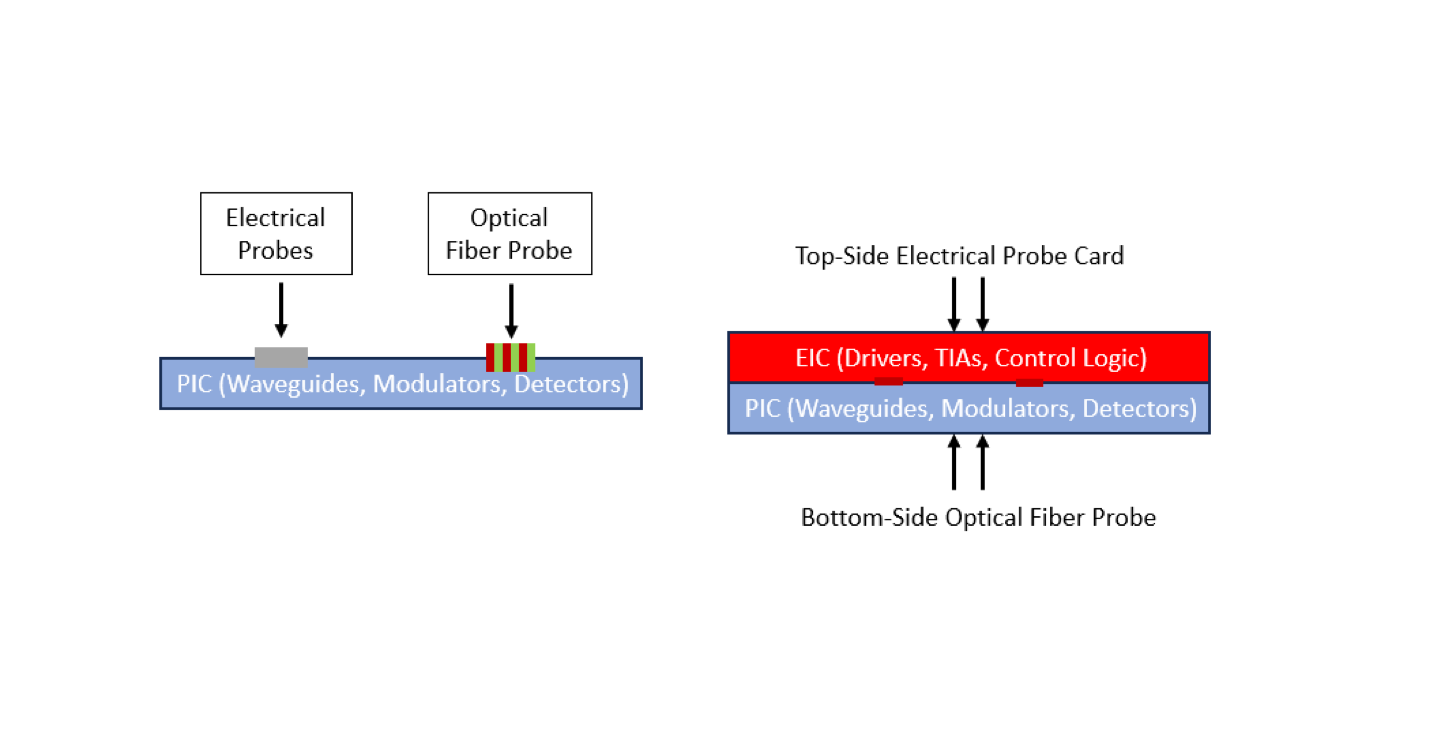
图 1|光测试自动化的两种基本形态:左侧为单面探测——电探针与光纤探针从同一侧作用于 PIC 晶圆;右侧为双面探测——EIC 从顶面走电探针卡,PIC 从底面走光纤探针。
Unlike electrical testing for semiconductors, automating optical test is extremely difficult because of the general finickiness of photonic designs, fragmentation of electronic - photonic design tools, and mechanical precision needed in the test equipment itself.
In order to enable high-volume testing of CPO, more automation is needed to automate existing semiconductor ATE equipment as much as possible. High-volume CPO test needs three forms of automation to coordinate together:
- Electrical ATE for EICs
- Optical instrumentation for PICs
- Mechanical automation for physical handling, precise alignment, and probing
Market Projections for Advanced Packaging and CPO
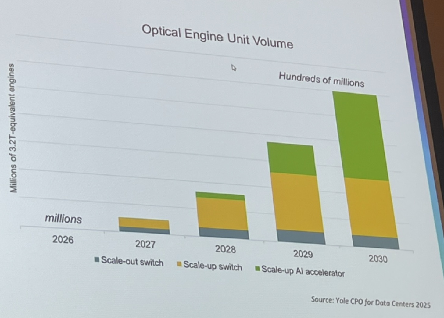
图 2|光引擎出货量预测(Yole CPO for Data Centers 2025):纵轴为等效 3.2T 光引擎的百万颗数。2026 年还以「百万颗」计,到 2030 年进入「数亿颗」区间,增量主要来自 scale-up AI 加速器与 scale-up 交换机。(原图标注:Source: G. Pereira. “Advanced Packaging as an Enabler of Co-Packaged Optics“ SiPh Packaging Summit 2026) In the next 5 years, both the advanced packaging and optical engine market are projected to grow rapidly due to the need for tighter integration and copper hitting a limit for data speeds. At the SiPh Packaging Summit, Yole projected a huge amount of growth in both markets:
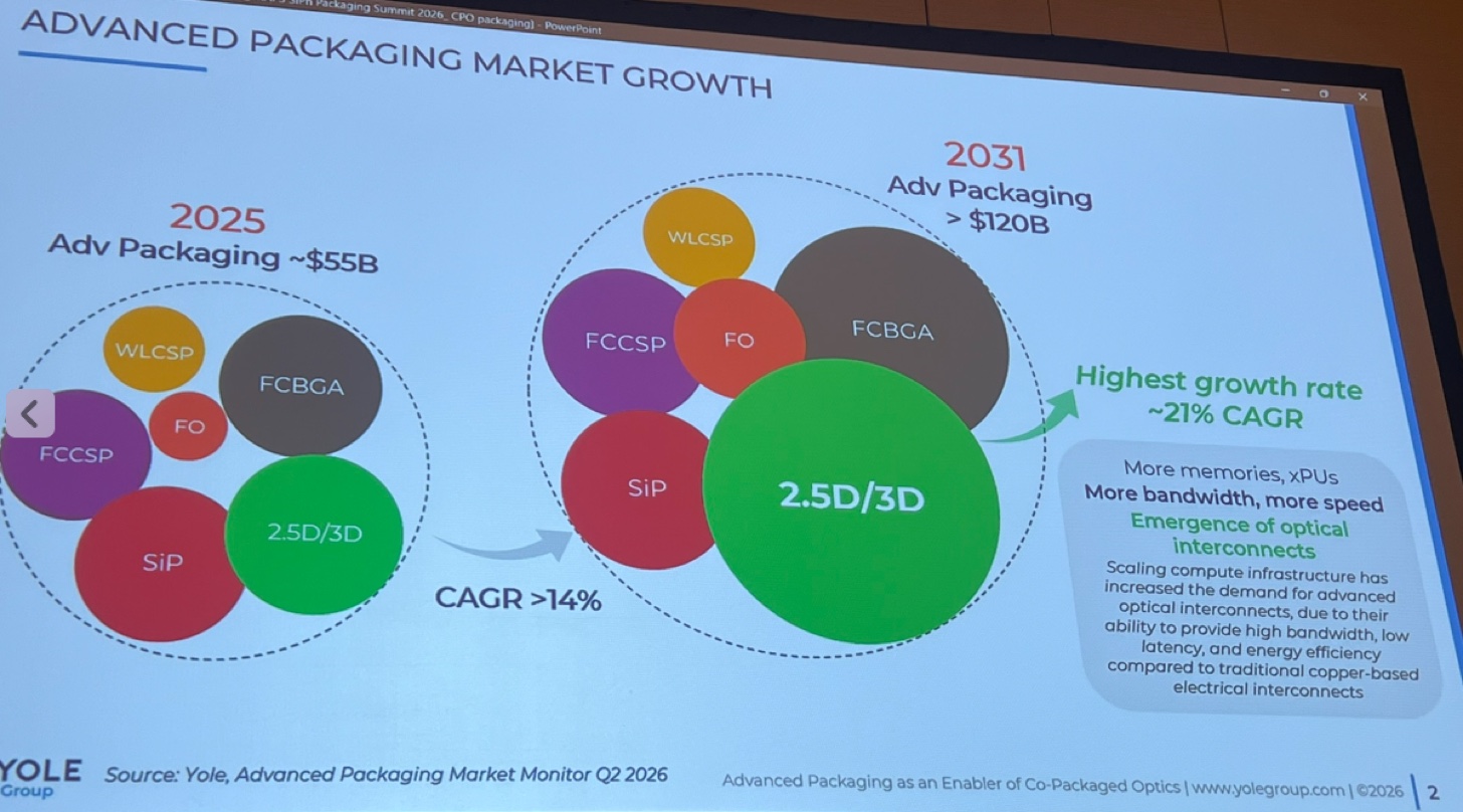
图 3|先进封装市场预测:2025 年 550 亿美元 → 2031 年超过 1,200 亿美元,CAGR >14%,其中 2.5D / 3D 部分 CAGR 约 21%。(原图标注:Source: G. Pereira. “Advanced Packaging as an Enabler of Co-Packaged Optics“ SiPh Packaging Summit 2026)
- The advanced packaging market expects growth from $55B in 2025 to >$120B in 2031 with a CAGR of >14%, with much of the growth driven by 2.5D / 3D at ~21% CAGR.
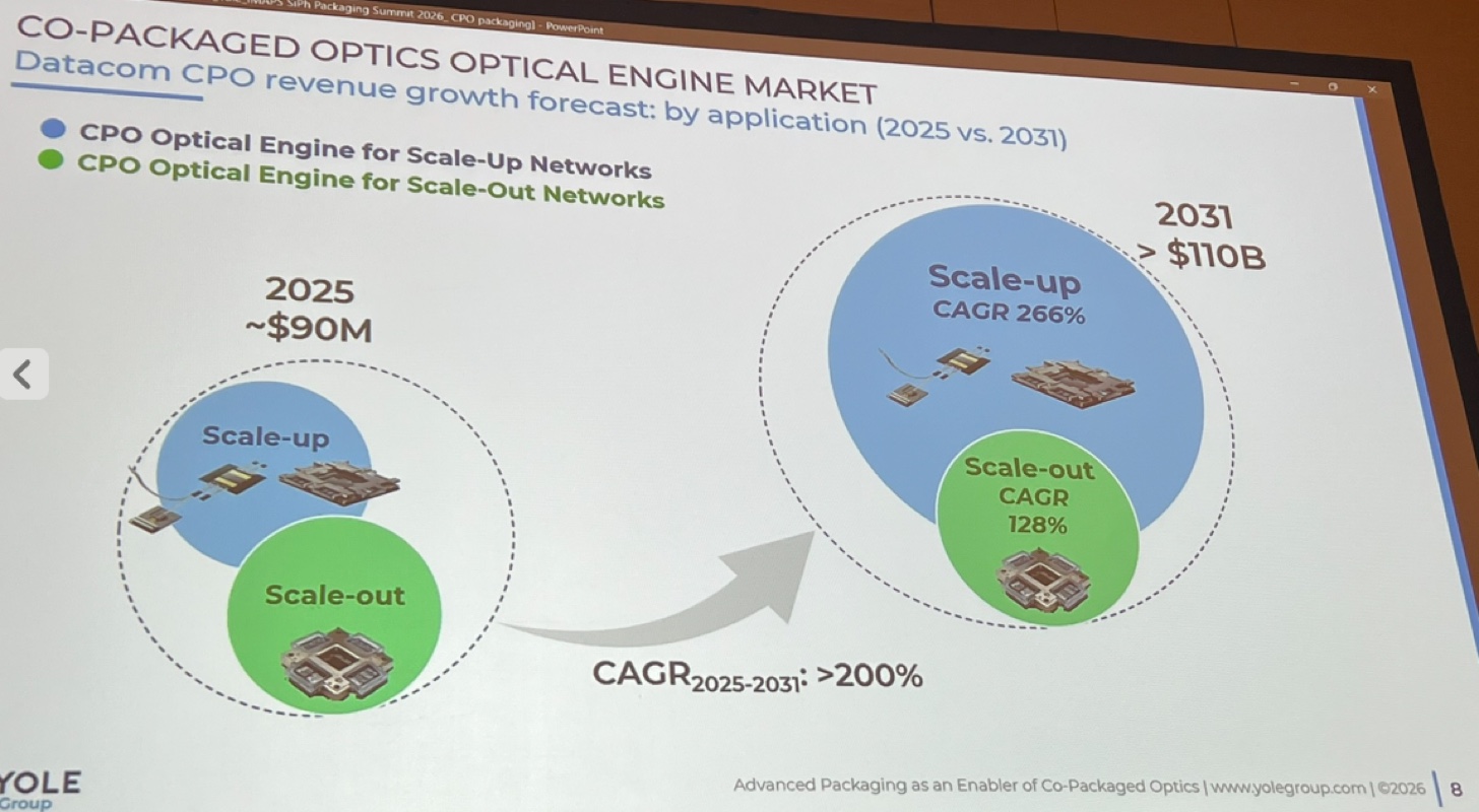
图 4|CPO 市场预测:2025 年约 9,000 万美元 → 2031 年 1,100 亿美元,CAGR >200%,且绝大部分增量落在 scale-up 场景。(原图标注:Source: G. Pereira. “Advanced Packaging as an Enabler of Co-Packaged Optics“ SiPh Packaging Summit 2026)
- The CPO market expects growth from ~$90M in 2025 to $110B by 2031, a >200% CAGR mostly dedicated to scale-up.
CPO was initially targeted for scale-out with CPO engines next to switch ASICs to address the faceplate limitations of LPO in large scale data networks. Then, CPO for scale-up / scale-in is following suit to address the BW limitations of copper. Karen Bergman, Professor, Columbia University notes how signals travelling off packaging pay a significant energy penalty and keeping signals on-package has a ridiculous bandwidth ceiling.
However, these market growth rates assume a few things:
- The optical test and measurement ecosystem scales to meet the demand. There is not a well-established, standardized high-volume optical test and measurement ecosystem yet.
- The underlying components have sufficient capacity to meet demand. InP substrate production and CPO fabrication throughput all must scale together to increase manufacturing throughput.
- The reliability of optics doesn’t cause hyperscalers to delay their adoption. CPO engines introduce new reliability risks, where laser failures with a high blast radius could take down a significant portion of a cluster. These risks must not outweigh the power and bandwidth benefits that CPO provides.
Technical Challenges with Optical Test and Measurement
While a lot of equipment and knowhow from semiconductor ATEs can be leveraged, integrating sensitive optical components is challenging. The optical domain tends to be isolated from the electrical domain, requiring equipment manufacturers to develop a broad understanding of how optical works to integrate it properly.
What makes optical test and measurement so challenging? I contend there are four major reasons:
- Precision needed for grating couplers and fibers. Grating couplers are optimized for lasers at a specific angle (typically 8-12 degrees). Single-mode optical fibers have sub-micron positioning tolerances (as low as < 0.5um) to minimize the IL penalty. In contrast, electrical probe needles have a mechanical spring compliance that allows them to scrub pads over a vertical range of 25-75um.
- Warpage on wafers makes precise alignment challenging. A single laser source at the same z-height will experience differing losses depending on the tilt and x-y offset of the wafer underneath.
- Cleanliness. Both dust particles in the air and on the surface block light and cause reflected power and distorted S-parameter measurements that cause otherwise good units to appear as failures. Optical testing environments need to be enclosed in clean environments with automated cleaning mechanisms such as N2 gas nozzles mounted next to optical probe heads.
- Lack of standardization across the optical ecosystem. There is virtually no standardization across several interfaces of the photonic packaging itself, including the optical I/O, optical engines, and optimization instruments. As a result, many CPO players are engaging in their own custom efforts that result in a lot of manual simulation of component libraries. Standardization can cut down on requirements gathering and custom efforts, enabling more market entrants for competitive solutions.
As photonics becomes more tightly integrated, manufacturing economics become increasingly dependent on finding defects earlier—before expensive components are combined.
Test Insertion Points: From Wafer to OE, CPO, and System
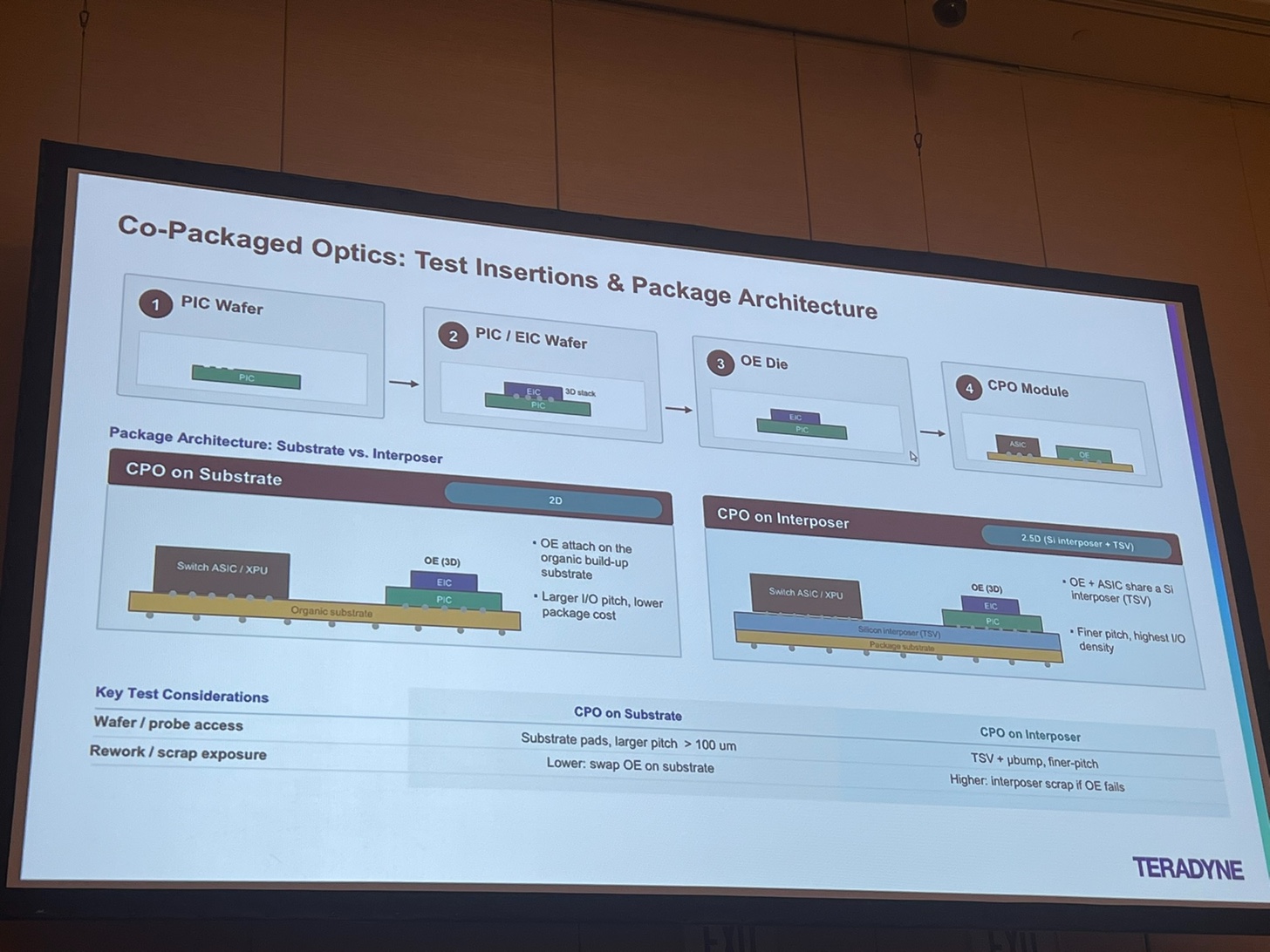
图 5|CPO 的四道测试插入点与两种封装架构(Teradyne):插入点 1 PIC 晶圆 → 2 PIC/EIC 晶圆 → 3 OE 裸片 → 4 CPO 模块。下半部分对比 CPO on Substrate 与 CPO on Interposer:衬底方案 pad 更大(>100 µm)、可在衬底上更换单个 OE,但翘曲更大、封装成本更高;中介层方案更小、IO 密度更高,但 OE 与算力芯片都焊死,不可返修。(原图标注:Source: M. Davis. “Enabling the AI revolution with high volume automated silicon photonics test solutions” SiPh Packaging Summit 2026) Co-packaged optics consist of multiple sophisticated components that must be connected together. Most OEs consist of a PIC and EIC typically hybrid bonded to each other. This OE is generally connected to either an organic substrate or interposer in a CPO module, but not always.
The testing process must be structured to filter out bad components early with known-good-die (KGD) screening. Bad components in fully assembled units are much more expensive to scrap if a failure is detected.
At each assembly step, electrical / optical stimuli are applied at different insertion points on the EIC and PIC. The performance results are measured and verified before integrating the component into higher-level assemblies. As components are integrated, some electrical and optical test interfaces can become inaccessible, making earlier screening with these test points increasingly important.
There are four common insertion points recognized by the industry:
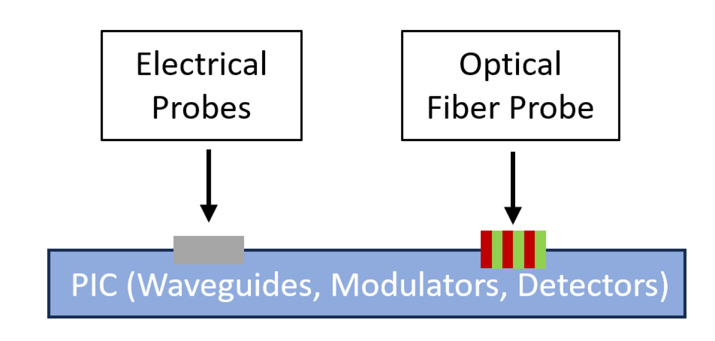
图 6|插入点 1:PIC 晶圆级单面探测——电探针与光纤探针从同一侧接触晶圆,在切割(D2W)与键合(W2W)之前先筛掉明显缺陷。
- Insertion 1: PIC Wafer. Wafer-level optical and/or electrical probing screens out gross defects before singulating the wafer for D2W and/or bonding the EIC and PIC wafer together for W2W. Depending on the PIC architecture, single-sided wafer probing uses both electrical and optical probes on the same side of the wafer.
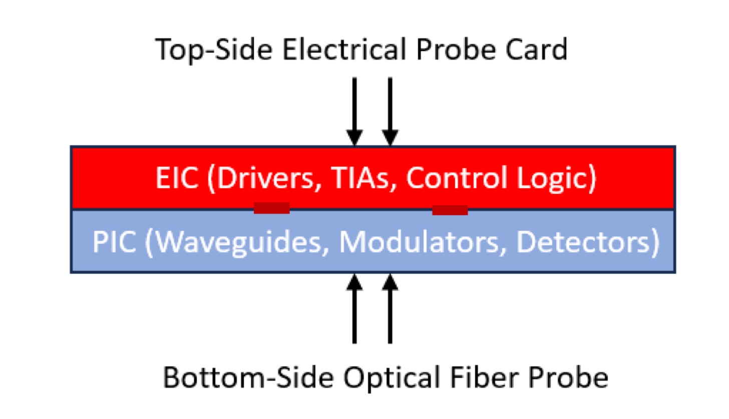
图 7|插入点 2:PIC/EIC 晶圆双面探测——EIC 从顶面走电探针卡,PIC 从底面走光纤探针。边耦合器、底面发光激光器、TSV 这类结构无法从顶面探针卡验证,只能翻过来从底面探。
- Insertion 2: PIC/EIC Wafer. Some hybrid-bonded OE architectures require double-sided probing, where the EIC can be probed with electrical probes on the top and the PIC with optical probes on the bottom. OEs can have a lot of features such as edge couplers, bottom-emitting lasers, and TSVs that are not easy to validate from a top-down probe card.
- Insertion 3: OE die. The diced and assembled OE subsystem is tested to ensure thermal reflow, epoxy curing, and mechanical placement didn’t degrade or misalign any optical components. This stage is where the known-good optical engine is established.
- Insertion 4: CPO Module. The assembled CPO system is tested for end-to-end electro-optical functionality, including link performance, BER, power, and thermal behavior.
Note that each stage is not simply a sequence of pass/fail stages, but rather a full-stack correlation. Losses accumulate where the measured loss at insertion 1 must be later cross-correlated with the performance of later insertions. This way, specific manufacturing steps can be scrutinized to sort out root causes of shifts or defects. Sufficient cross-correlation data gives confidence to the customer that the photonic models are sufficient. This type of work typically falls under product engineering to monitor the lifecycle of the assembly process and optimize the process.
Optical Engine Requirements
The OE contains the bulk of the high-speed optical and electrical components - modulators, photodetectors, EICs, and coupling interfaces. This OE often interfaces with a detachable FAU that can have up to hundreds of fibers. During assembly, the OE itself is mounted on a thermal chuck that can adjust from cold to hot temperatures to test the OE in the expected thermal environment.
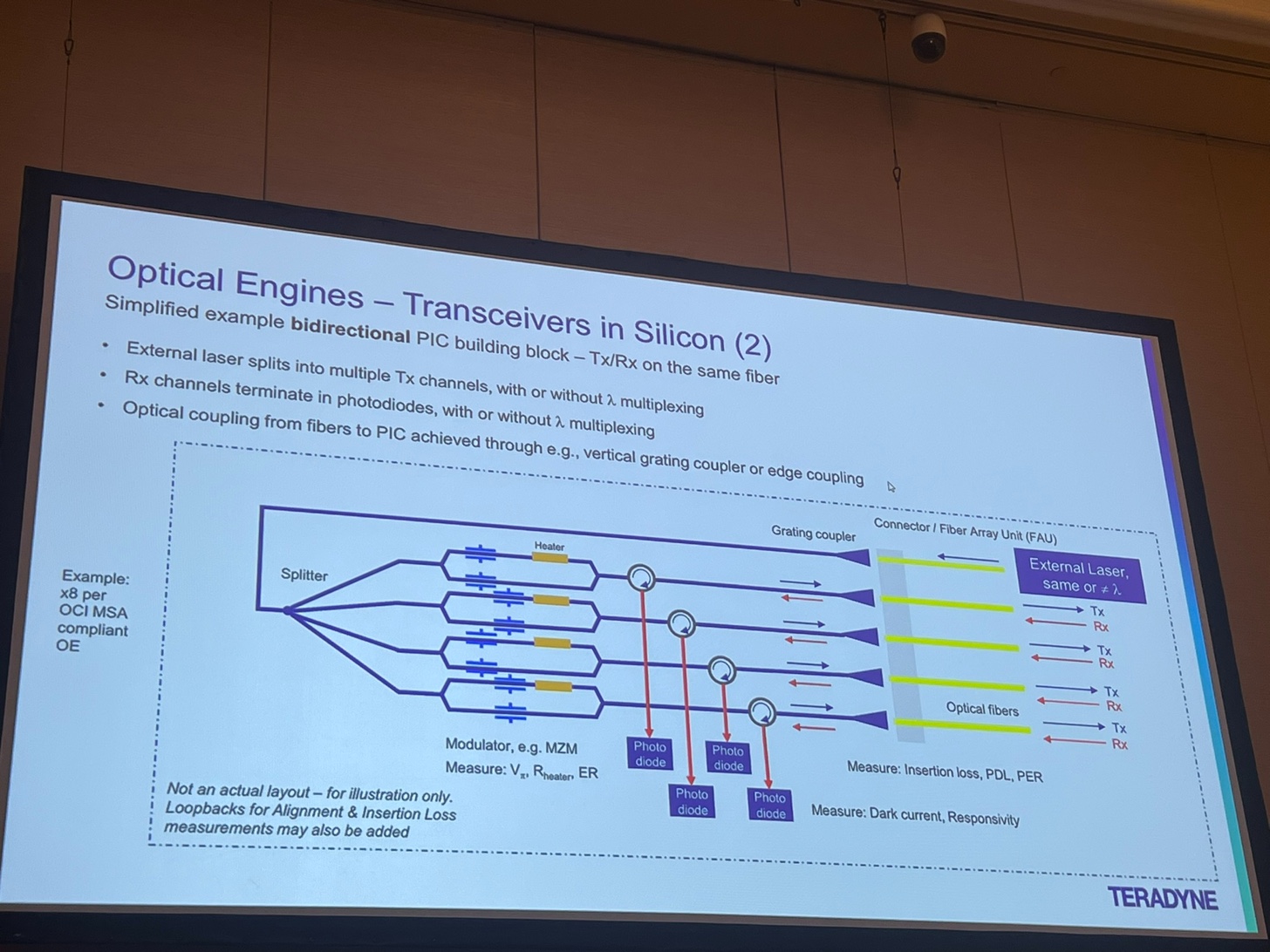
图 8|现代双向 PIC 测试积木(Teradyne):外部激光经分束器分为多路 TX 通道,光栅耦合器 / 边耦合器完成光纤与芯片之间的耦合,调制器(如 MZM)由 EIC 驱动;本例中环行器在 TX 调制器与 RX 光电二极管之间切换通道。(原图标注:Source: M. Davis. “Enabling the AI revolution with high volume automated silicon photonics test solutions” SiPh Packaging Summit 2026) Here is a high-level example of a modern bidirectional PIC building block to test. Light comes in through optical fibers onto a grating coupler and is then manipulated through modulators that are driven by an EIC driver. In this example, a circulator swaps channels between modulators for TX and photodiodes for RX.
A successful test setup must be able to apply a constant laser stimulus, adjust a “knob” in the electrical or optical domain, and measure the resulting optical output and/or PD output. Examples of measured parameters include:
- Spectral performance across wavelength bands
- Insertion loss
- Modulator device tuning
- Photodiode parameters (dark current, responsivity)
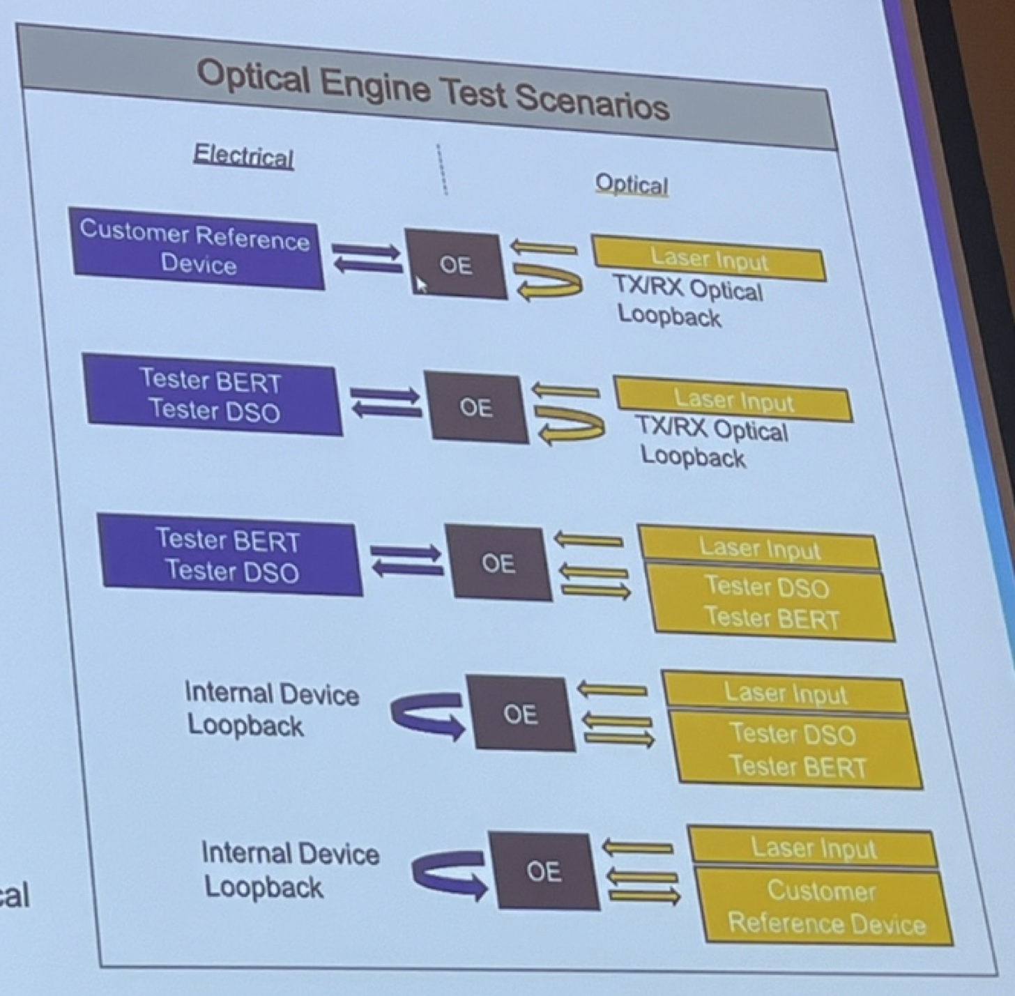
图 9|光引擎的五种常见测试场景(Teradyne):客户参考器件验证、ATE 电学表征、全电光收发表征、光域表征,以及不带主机板的系统仿真(对未来标准化光 I/O chiplet 尤为重要)。(原图标注:Source: M. Davis. “Enabling the AI revolution with high volume automated silicon photonics test solutions” SiPh Packaging Summit 2026) The optical engine undergoes a few testing scenarios to verify device-level and system-level functionality. There are five common test scenarios that combine both electrical and optical functionality:
- Host System Validation: The OE is connected to the customer reference device it is expected to interface with (such as an ASIC). A laser input is applied and the TX/RX is looped back to validate that customer’s host board can successfully communicate with the OE.
- Electrical ATE Characterization: The optical TX/RX is looped back. The electrical input is driven by an ATE and its electrical output measured after traversing the E-O-E link. This measures system-level parameters such as link margin, BER, and electrical eye quality with standard ATE equipment.
- Full Electro-Optical Transceiver Characterization. This tests the E-O and O-E paths simultaneously.
- Optical Characterization. Loop back the electrical side and test the optical path.
- Optical System Emulation. Hook a customer reference optical device (such as an optical tester or reference switch) to test for interoperability w/o a host electrical board attached. This is important for standardized optical I/O chiplets like Ayar Labs is doing.
These results are all correlated with each other to isolate nonidealities on either the electrical or optical TX/RX side.
The test setup itself provides the lasers, power supplies, and digital communications for 224Gbps+. OEs requires several pieces of test equipment:
- High-speed RF testers such as a BERT (bit error rate tester)
- Digital sampling oscilloscopes (DSO)
- Active fiber / connector alignment - this includes either direct fiber alignment or automated connectors interfacing with emerging vendor standards such as Senko, Teramount, Ranovus, FOCI, or Corning.
- Handling equipment with fine accuracy for both wafer-level handling and die/OE handling. These use edge grip or vacuum pressure so the handling arm doesn’t damage the die / wafer surface.
Single-sided electro-optical probe cards. Product-specific probe cards provide the electrical interface between the SiPh wafer and existing ATE, while precision optical probes/fiber arrays couple light into and out of the device. FormFactor is a leading supplier of wafer-level SiPh electro-optical probing and test interfaces.
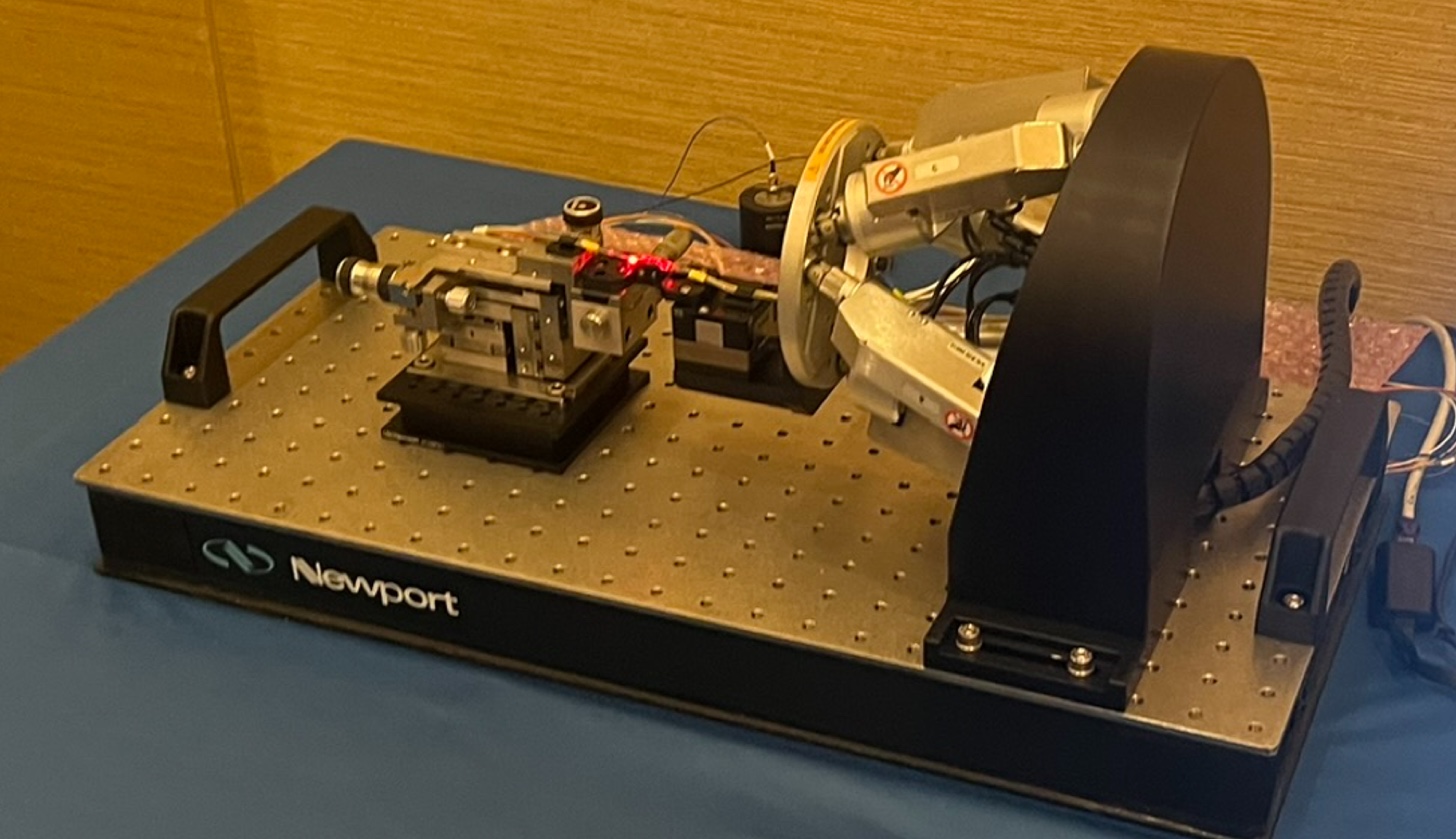
图 10|六足平台(hexapod)光纤阵列对准示例(MKS Newport):光学探针需要 5–6 个自由度(X / Y / Z 加三个旋转轴),才能按特定角度把激光耦合进光栅耦合器。
- Hexapods / piezo drivers for precision alignment. Optical probes require 5 or 6 degrees of freedom (X, Y, Z, ϴx, ϴy, ϴz) to align lasers on grating couplers at specific angles. Here is an example of a hexapod fiber array alignment from MKS’s Newport brand for rapid, nm-level alignment for wafer-level probing and testing, multi-channel array alignment, fiber-to-chip coupling, and photonic device assembly and packaging.
I believe that the alignment time of optical components will bottleneck test time. I also expect to see the demand of underlying subcomponents rise along with the growth of automated testing solutions.
Co-Packaged Optics Module Requirements
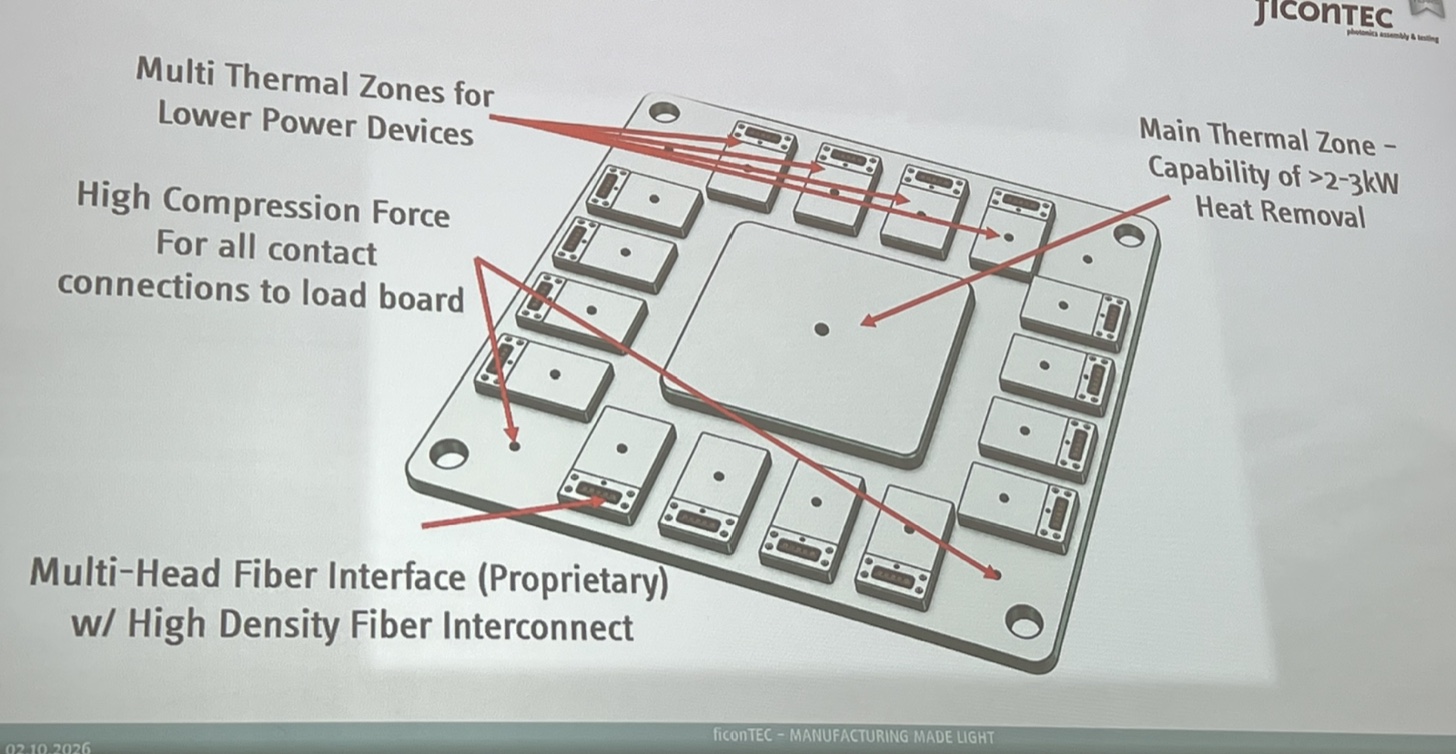
图 11|CPO 插座 / 载板设计(Jicotec):多热区设计为低功耗器件单独控温,主热区需具备 >2–3 kW 的散热能力;全部接触点需要高压缩力,另外还有专有的多头高密度光纤互连接口。(原图标注:Source: R. Ghane. “From Demonstration to Deployment: Overcoming the Manufacturing and Test Bottlenecks of Silicon Photonics and Co-Packaged Optics for AI Infrastructure” SiPh Packaging Summit 2026) At insertion 4, co-packaged optics typically integrate 4 - 16 known-good optical engines onto a shared substrate or CPO socket with massive compute silicon. Testing at this stage needs to ensure that the entire system works as expected. Failures here are expensive since the entire module is scrapped, so it is important that only known-good optical engines are mounted at this stage.
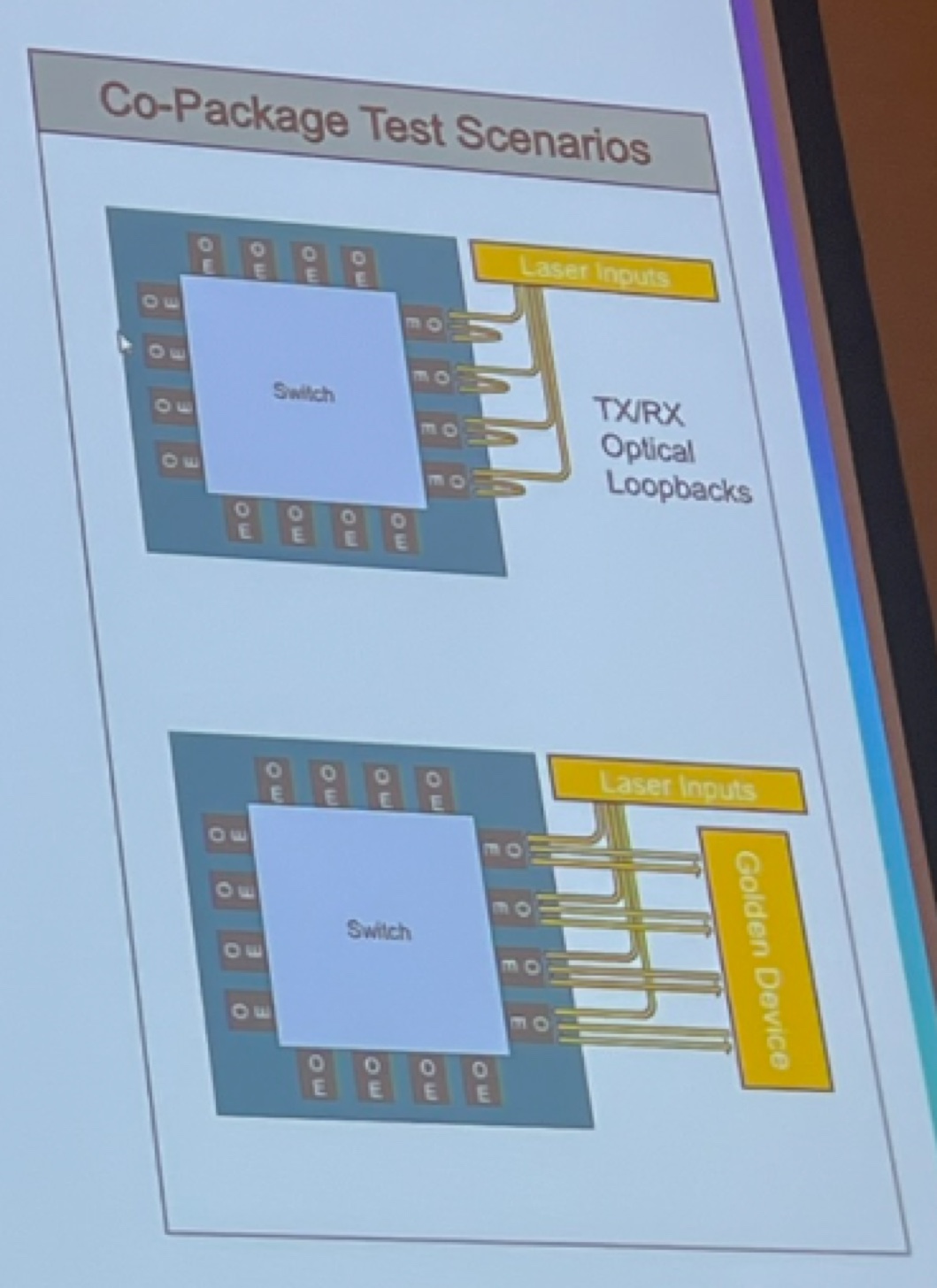
图 12|CPO 模块级测试场景(Teradyne):上路为 TX/RX 光回环,下路引入一颗「黄金器件(golden device)」作参照——回环无法区分究竟 TX 坏还是 RX 坏,只有黄金器件才能把故障定位到具体一侧。(原图标注:Source: M. Davis. “Enabling the AI revolution with high volume automated silicon photonics test solutions” SiPh Packaging Summit 2026) Testing scenarios at this stage are more system-level tests such as how the OE interacts with the fiber interface and CPO socket. There are various fidelities of test, ranging from optical-engine performance checks to ensure nothing was degraded during assembly, to more complete ‘mission-mode’ tests that stress system-level functionality.
There are several test considerations:
- In some CPO architectures, a switch may contain up to 16 OEs, with each OE requiring multiple CW laser inputs. A configuration of 4 - 8 independent continuous wave lasers require a total of 64 - 128 lasers to be supplied during test.
- Thermal management - CPO modules must maintain performance while also simultaneously handling package power dissipation
- Each package side can have up to hundreds of individual fibers with varying connector standards that must be aligned accurately by mechanical connector actuators
- A golden DUT can be used to isolate whether failures and/or performance degradation are due to the TX or RX side. Loopbacks can’t isolate whether TX and/or RX is bad.
Test and Measurement Equipment Covering all Four Insertions
There are already established equipment suppliers for high-volume testing of SiPh today. In general, the trend is moving toward a platform-based approach with modular building blocks to automate as much of the steps as possible.
There are two competing strategies:
—— 付费墙分割线 ——
公开段到此结束。原文在「There are two competing strategies:」之后继续讨论两种设备策略的对比,该部分属付费内容,本页未含。
第二部分:中文深度解读
一句话结论
这篇文章不是在讲「光测试很难」这种泛泛之谈,而是在指出一件更硬的事:CPO 的市场预测建立在测试生态能同步放大的假设之上,而这个假设目前没有任何证据。作者把「光测试与测量生态能扩产到位」直接列为市场增长率成立的前置条件之一——这等于自己承认了整条 CPO 叙事里最薄的一环。
核心主张拆解
原文的主线只有三句话:
- 光测试自动化天生比电测试难,难点是物理性的,不是工程投入能线性堆出来的。
- 解法是把测试拆成四道插入点,在组件还便宜的时候就筛掉坏品,且四道之间必须做「全栈相关性」而非各自独立 pass/fail。
- 设备生态已经在成形,趋势是平台化 + 模块化积木,但标准化几乎为零。
值得注意的是作者的收尾判断:「对齐时间会成为测试时间的瓶颈」。这一句放在全文最后、且用粗体标出,是整篇文章里唯一一个明确的预测性断言——它比任何市场数字都更值得记住。
因果链:为什么测试是 CPO 的闸门
原文给出的逻辑链可以还原成四步:
- 铜的带宽天花板逼迫信号进封装 → CPO 从 scale-out 扩展到 scale-up / scale-in。
- 封装越紧,组合出来的价值越贵(4–16 颗 KGD 光引擎 + 大算力硅 + 载板),一次报废的代价呈数量级上升。
- 于是必须把缺陷往前赶,在 PIC 晶圆阶段就筛掉 → 四道插入点结构。
- 而四道插入点的每一道都涉及光学对准,光学对准的物理公差比电学严 1–2 个数量级 → 测试时间与成本被卡在这里。
这条链的薄弱处在第 4 步:前三步都是行业共识,第 4 步是作者的判断,而且文章自己也没给出任何测试节拍或单颗测试成本的数字来支撑。
四道插入点:缺陷发现越早越便宜
原文把这套流程讲得比较散,我把它整理成一张对照表:
| 插入点 | 阶段 | 测什么 | 关键约束 |
|---|---|---|---|
| 1 | PIC 晶圆 | 晶圆级光/电探测,筛掉明显缺陷 | 单面探测:电探针与光纤探针同侧 |
| 2 | PIC/EIC 晶圆 | 混合键合后的双面探测 | EIC 从顶面走电探针卡,PIC 从底面走光纤探针(边耦合器、底面发光激光器、TSV 顶面看不到) |
| 3 | OE 裸片 | 切割与组装后的子系统 | 确认热回流、环氧固化、机械贴装没有让光学件退化或失准——这是「已知良好光引擎(KGOE)」的判定点 |
| 4 | CPO 模块 | 端到端电光功能:链路性能、BER、功耗、热行为 | 4–16 颗 KGD 光引擎上共用衬底/插座,报废即整模块报废 |
原文特别强调:这四道不是简单的 pass/fail 序列,而是全栈相关性(full-stack correlation)。插入点 1 测到的损耗,必须在后续插入点做交叉关联,才能反推是哪一道制造工序出了问题。这句话的工程含义是:测试数据要能纵向串起来,而不只是产出四个独立的良率数字。文中指出这类工作通常归口产品工程(product engineering),用于监控整个组装流程的生命周期并优化工艺——这是一个容易被忽略的组织能力要求。
市场数字的口径检查
原文引用的三个数字,我逐个做了算术核对:
| 指标 | 2025 | 2031 | 隐含 CAGR | 核对结果 |
|---|---|---|---|---|
| 先进封装市场 | $55B | >$120B | 原文称 >14% | 实算约 13.9%,与原文一致 ✅ |
| CPO 市场 | 约 $90M | $110B | 原文称 >200% | 实算约 227%,与原文一致 ✅ |
| 光引擎出货量 | 2026 年「百万颗」级 | 2030 年「数亿颗」级 | 未给出 | 约合每年 3 倍量级 |
算术没错,但有两个口径问题必须点出来:
- CPO 市场的起点只有约 9,000 万美元。这是一个极小的基数,「>200% CAGR」几乎完全由低基数决定,不能被读作需求的确定性。而且 2031 年的 1,100 亿美元,与同期先进封装市场的 1,200 亿美元是同一量级——这意味着该预测里已经内嵌了「CPO 成为主流封装形态」这个远未兑现的假设。
- 光引擎出货量从「百万颗」到「数亿颗」,如果真要落地,测试产能必须同比例放大。原文把这一条明确列为市场增长率的成立前提(「光测试与测量生态必须扩产到位」),措辞是「目前还没有一个成熟、标准化的高量产光测试与测量生态」。
原文还列了另外两个前提:InP 衬底产能与 CPO 制造吞吐必须一起放大;以及光学的可靠性不能让超大规模厂商推迟采用——后者提到「激光失效的高爆炸半径(high blast radius)可能一次性打掉集群的相当一部分」。这一条在公开段只有一句话,但它其实是 CPO 商业模式里最涉及钱的假设,值得单独留意。
光学测试为什么难:四个物理原因
这是全篇最有信息量的一节。作者给了四条理由,我做了归类和对比:
| 原因 | 具体物理约束 | 与电学的对比 |
|---|---|---|
| 对准精度 | 光栅耦合器要求激光以 8–12° 的特定角度入射;单模光纤为压低插损需要亚微米级定位公差(低至 0.5 µm 以下) | 电探针针尖靠机械弹簧顺应性,可以在 25–75 µm 的垂直范围内「刮擦」焊盘完成接触——电学的「蛮力接触」策略在光学上完全不成立 |
| 晶圆翘曲 | 同一 z 高度的激光源,会因晶圆下方的倾斜与 x-y 偏移而产生不同损耗 | 电探针的弹簧余量可以吸收翘曲,光学不行,必须逐点动态对准 |
| 洁净度 | 空气中的尘粒与表面的尘粒同时挡光并产生反射功率,造成 S 参数畸变,把好品判成坏品 | 需要封闭洁净环境 + 自动清洁机制(如探针头上并排安装 N2 气嘴) |
| 标准缺失 | 光 I/O、光引擎、优化仪器几乎都没有统一接口标准 | 结果就是各家自研、大量手工搭建元器件库 |
这四条里,第 4 条(标准缺失)是最有产业杠杆的一条,因为它不改变物理极限,却能显著改变成本结构——原文的原话是标准化可以减少需求收集与定制工作量,「让更多市场参与者带来有竞争力的方案」。第 1 条则解释了为什么「对准」会成为作者预判的瓶颈:如果每次耦合都要在 0.5 µm 的尺度上重新搜索角度和位置,那么它就很难被并行化。
第三、四条隐含一个容易被忽略的推论:光学测试的「过杀(overkill)」风险高于电学测试。尘粒导致的畸变会把好品判成坏品,这在良率爬坡期会直接放大成本——而 KGD 筛选的前提正是「筛选本身不能太贵」。
设备生态地图
原文点名的厂商,按环节整理如下(仅收录原文明确提到的):
| 环节 | 原文提到的厂商 | 说明 |
|---|---|---|
| 晶圆级硅光电光探测与测试接口 | FormFactor | 原文称为该领域的领先供应商,提供产品专用探针卡(电接口)与精密光学探针/光纤阵列(光耦合) |
| 主动光纤 / 连接器对准 | Senko、Teramount、Ranovus、FOCI、Corning | 用于直接光纤对准,或对接新兴厂商标准的自动连接器 |
| 精密对准运动平台 | MKS 的 Newport 品牌 | 六足(hexapod)/ 压电驱动,提供 5–6 个自由度与 nm 级对准 |
| 高速 RF 与误码测试 | BERT(误码仪)、DSO(数字采样示波器) | 支撑 224 Gbps 以上的测试设置 |
| 测试机 / 自动化平台 | 原文提到 Teradyne 的幻灯片为多张图的来源 | 四道插入点与测试场景的框架图均出自 Teradyne |
原文最后一段指出:高量产硅光测试已经有成型的设备供应商,趋势是走向「平台化 + 模块化积木」。然后文章就进入了付费段——「There are two competing strategies:」之后的两种策略对比,本页未含,无法核对。这是本文最大的信息缺口:整篇文章的落脚点恰好被付费墙切掉了。
我的评述
第一,这篇文章真正的贡献是把「测试」从配套问题提升为结构性问题。 站内此前的测试类文章(如 SENKO / Advantest / VIAVI 那篇)讲的是模块级测试的「连接器 + 自动化环境 + 测试仪」三方分工;这篇则给出了从晶圆到模块的四道插入点全景,两者是互补的:前者回答「模块级怎么测」,后者回答「在整个制造流程里该在哪几个位置测、以及为什么必须在这几个位置测」。
第二,「全栈相关性」这个提法比插入点本身更有价值。 如果四道插入点各自独立打卡,得到的是四个割裂的良率数字;只有把插入点 1 的损耗与后续插入点的性能交叉关联,才能反推是哪道工序出了问题。这意味着测试体系的核心资产其实是纵向可比的数据链,而不是测试机台本身——这个判断对评估相关公司的护城河很重要。
第三,我做了一个粗略的时间量级推算(属解读者推算,原文未给出任何时间数字)。 原文给出的规模是:一个交换机最多 16 个 OE,测试时需同时供给 64–128 路连续波激光;每个封装面最多有数百根连接标准各异的光纤。若按每路激光对准 1 秒的乐观假设,仅激光注入对准就是 1–2 分钟;若数百根光纤逐根对准、每根 1 秒,就是数分钟到十余分钟。而「高量产」对 CPO 模块测试的节拍要求必然是分钟级甚至更低。这个量级上的张力,正是作者说「对齐时间会成为瓶颈」的算术基础。 需要强调的是:这个推算的每一环都可能被并行化或自动化改写,所以它只用来标定问题的量级,不能当作结论。
第四,可靠性那一句话的分量被低估了。 「激光失效的高爆炸半径」意味着 CPO 的失效率不是按端口计,而是可能按集群份额计。在一个动辄数万 XPU 的部署里,这会直接改变超大规模厂商的采购决策权重——它比功耗与带宽收益更容易触发「推迟采用」。原文只写了一句就过去了,但这可能是整篇里最贵的一句话。
可采信度分层
| 层级 | 内容 | 理由 |
|---|---|---|
| 强 | 四条光学测试难点的物理约束;四道插入点的划分;缺陷越早发现成本越低的制造经济学 | 物理约束可独立验证;插入点划分是行业共识,Teradyne / FormFactor 等厂商表述一致 |
| 中 | Yole 的市场预测数字;插入点各阶段的测试项清单;设备供应商的具体归属 | 第三方机构与单一厂商的 self-report,口径未公开,且以厂商自身产品线视角组织 |
| 弱 | 「对齐时间会成为测试时间的瓶颈」;「市场增长率依赖测试生态扩产」 | 作者的判断与推理,有行业直觉价值,但文中没有提供测试节拍、良率或成本数据支撑 |
| 未含 | 付费段「两种竞争策略」的具体内容(约 370 词);所有测试时间、良率与成本数字 | 付费墙截断;原文公开段本身也未给出此类数据 |
这篇文章没有回答什么
- 没有测试时间与成本的绝对数字——没有节拍(UPH)、没有单颗测试成本、没有测试占总成本的比例。作者提出「对齐时间会成瓶颈」,但没有给出任何基线。
- 没有良率数字——PIC 晶圆级良率、混合键合后良率、模块级良率全部缺失,因此无法量化「提前筛选」到底省了多少钱。
- 没有把测试产能与市场预测做定量对账——「2030 年数亿颗光引擎」需要多少台探针台、多少个洁净对位工位,文章没有算。
- 没有对比「不测」的代价——逃逸(escape)到现场的失效率与成本没有讨论,而这正是 KGD 投入的经济性论证。
- 付费墙后的两种设备策略对比缺失——恰好是全文的落脚点。
- 激光可靠性的爆炸半径只写了一句,没有展开失效率假设与故障域划分。
对工程与投资的启示
- 把测试设备与接口环节单独看待,而不是笼统归入「CPO 供应链」。四道插入点意味着测试是一个跨晶圆、裸片、模块的多环节资产,其复杂度不低于封装本身。
- 对准自动化程度是关键的差异化变量。谁能把 nm 级光纤/激光对位做成高量产节拍,谁就掌握了这道闸门。原文点名的 FormFactor(探针卡与接口)、MKS Newport(六足/压电平台)、以及 Senko / Teramount / Ranovus / FOCI / Corning(连接器对准)都值得按这个维度重估。
- 标准化是降本的最大杠杆,而且它不依赖物理突破。站内此前记录的 OIF 与 NPO 标准化进展,恰好可以从这个角度重读——标准化的价值不只是互操作,还包括砍掉各家自研的元器件库与手工仿真成本。
- 把「全栈相关性」当作尽调问题:不要问对方「测不测」,而要问「四道插入点的数据能不能纵向串起来」。这决定了对方能不能收敛工艺,而不只是筛出坏品。
与站内文章的联系
- SENKO、Advantest 与 VIAVI 攻克 CPO 模块级测试的隐藏瓶颈——本文的插入点 4 与那篇的模块级测试是同一问题的两个视角,建议对照阅读。
- SEMICON Taiwan 2026 CPO 全记录——那篇提到「测试产能决定时间表」,本文给出了这句话的物理与技术细节。
- 华为 OIF / NPO 标准化与 7.2T 模块 与 NewPhotonics:走向 CPO / NPO 之路——本文把「标准缺失」列为四大难点之一,这两篇提供了标准化进程的产业侧进展。
- CPO 224 Gbps 一体化方案综述——本文提到的 224 Gbps 以上测试设置与那篇的技术路线直接相关。
- 在实践中做参数化良率——「全栈相关性」本质上是参数化良率方法在光电耦合场景的延伸。
一句话总结
这篇文章最值钱的地方不是那三个市场数字,而是它自己承认了那三个数字的前提——光测试生态必须先扩产到位,而目前既没有标准化,也没有成熟的高量产方案;同时它给出了一个可检验的预测:对齐时间会成为测试节拍的天花板。至于「两种竞争策略」究竟是什么,恰好被付费墙挡住了。