From Taylor Series to Silicon: Building and Debugging a ROM-less CORDIC — 从泰勒级数到硅:构建并调试一个无 ROM 的 CORDIC
逐译 Rohan Verma 在 Bit Banging Bytes 的 ROM-less CORDIC 流片实战:如何用泰勒级数在硬件里生成反正切微旋转角、首硅误差结构拆解(20 码相位偏差的方形波指纹),以及仅靠 SPI 包里的两个常量把平均绝对误差从 13.5 LSB 降到 1.71 LSB、RMS 改善 6.8×。
原文:Rohan Verma《From Taylor Series to Silicon: Building and Debugging a ROM-less CORDIC》(Bit Banging Bytes,2026-08-16)| 英文原文 + 中文深度解读。 原文链接:https://bitbangingbytes.substack.com/p/from-taylor-series-to-silicon-building 本文为「英文原文 + 中文深度解读」两层结构,全部配图已本地化(原图来自 substack-post-media S3 直链)。 原文无付费墙,全文已取得。
第一部分:正文(Original Article)
From Taylor Series to Silicon: Building and Debugging a ROM-less CORDIC
How we fixed our chip by lying to it
Rohan Verma · Bit Banging Bytes · Aug 16, 2026
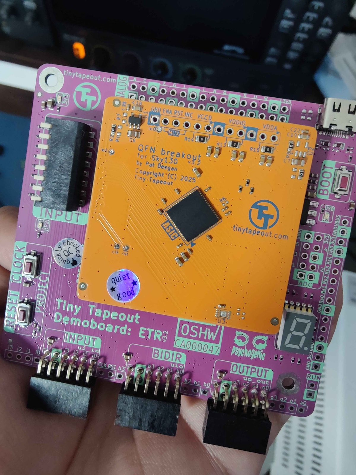
Last year we taped out a ROM-less CORDIC engine on the Tiny Tapeout sky25a shuttle: a 2×2 tile on SkyWater’s sky130 process, computing sin and cos of a 16-bit fixed-point angle over SPI. The silicon is back and it works. First full 0–360° sweep, 100 out of 100 angles passed.
This project started with a fairly simple goal: build a CORDIC engine small enough to fit comfortably into a Tiny Tapeout ASIC, without spending silicon area on a ROM full of arctangent constants.
There is something deeply satisfying about making a mathematical function run in hardware. You start with an equation. Then you turn it into an algorithm. Then RTL. Then gates. Then, eventually, you are staring at a physical chip wondering whether the thing you wrote almost a year ago actually works.
On a software project you find the bug, patch it, move on. On silicon the bug is printed. You live with it, you re-spin (months, real money), or you find a back door.
This post is about the back door, but it starts with the design, because the back door only exists thanks to one decision made at design time. The fix that shipped is two constants in the SPI packet. Mean error down 7.9×, RMS down 6.8×. Getting there took some careful error decomposition, plus a detour through an unrelated SPI problem where every value the chip returned was exactly half of the right answer.
Why CORDIC?
CORDIC—Coordinate Rotation Digital Computer—is one of those algorithms that looks almost suspiciously well suited to hardware.
Instead of calculating sine and cosine using multipliers, divisions, or large lookup tables, CORDIC repeatedly performs very simple operations:
- add/subtract
- arithmetic shifts
- compare the accumulated angle
At each iteration, the vector is rotated by an elementary angle: atan(2⁻ⁱ).
The corresponding iteration can be written approximately as:
\[x_{i+1} = x_i - \sigma_i (y_i \gg i)\] \[y_{i+1} = y_i + \sigma_i (x_i \gg i)\] \[z_{i+1} = z_i - \sigma_i \theta_i\]where $\theta_i = \text{atan}(2^{-i})$ and $\sigma_i \in {-1, +1}$ determines the direction of rotation. This is exactly the kind of arithmetic digital hardware likes.
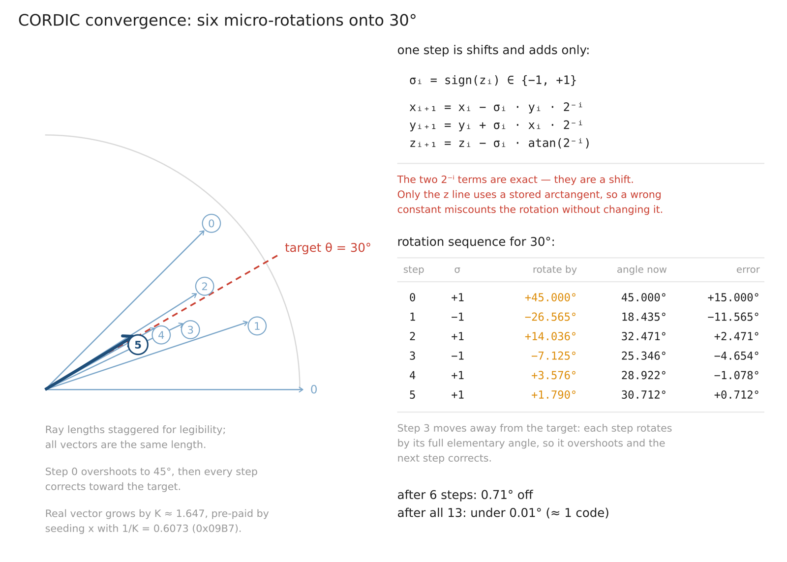
Each micro-rotation is by a fixed elementary angle atan(2⁻ⁱ), chosen because rotating by that particular angle costs only shifts and adds, no multipliers. Pick the direction of each rotation from the sign of the remaining angle, run the iterations, and the vector converges onto (cos θ, sin θ). It’s the algorithm inside decades of calculators and DDS chips, and it needs exactly one lookup table: the list of elementary angles.
But there is a catch.
The algorithm needs the elementary angles.
The conventional implementation therefore has a small lookup table containing values such as:
1
2
3
4
atan(1)   = 0.785398...
atan(1/2) = 0.463647...
atan(1/4) = 0.244979...
atan(1/8) = 0.124355...
On an FPGA, throwing a ROM at this problem is easy.
On a tiny ASIC?
Every bit of storage matters.
So we asked a slightly annoying question:
Can we get rid of the ROM entirely?
The ROM-less idea
The key observation is that the elementary angles become extremely well behaved as the iteration number increases.
For small $x$,
\[\arctan(x) = x - \frac{x^3}{3} + \frac{x^5}{5} - \cdots\]and our CORDIC only needs $x = 2^{-i}$.
So instead of storing a table, we can generate the elementary angles mathematically.
The first few values are the difficult ones.
After that, $2^{-i}$ becomes such a good approximation to atan($2^{-i}$) at our 12-bit fractional precision that the difference effectively disappears after quantization.
The exact values used for comparison are:
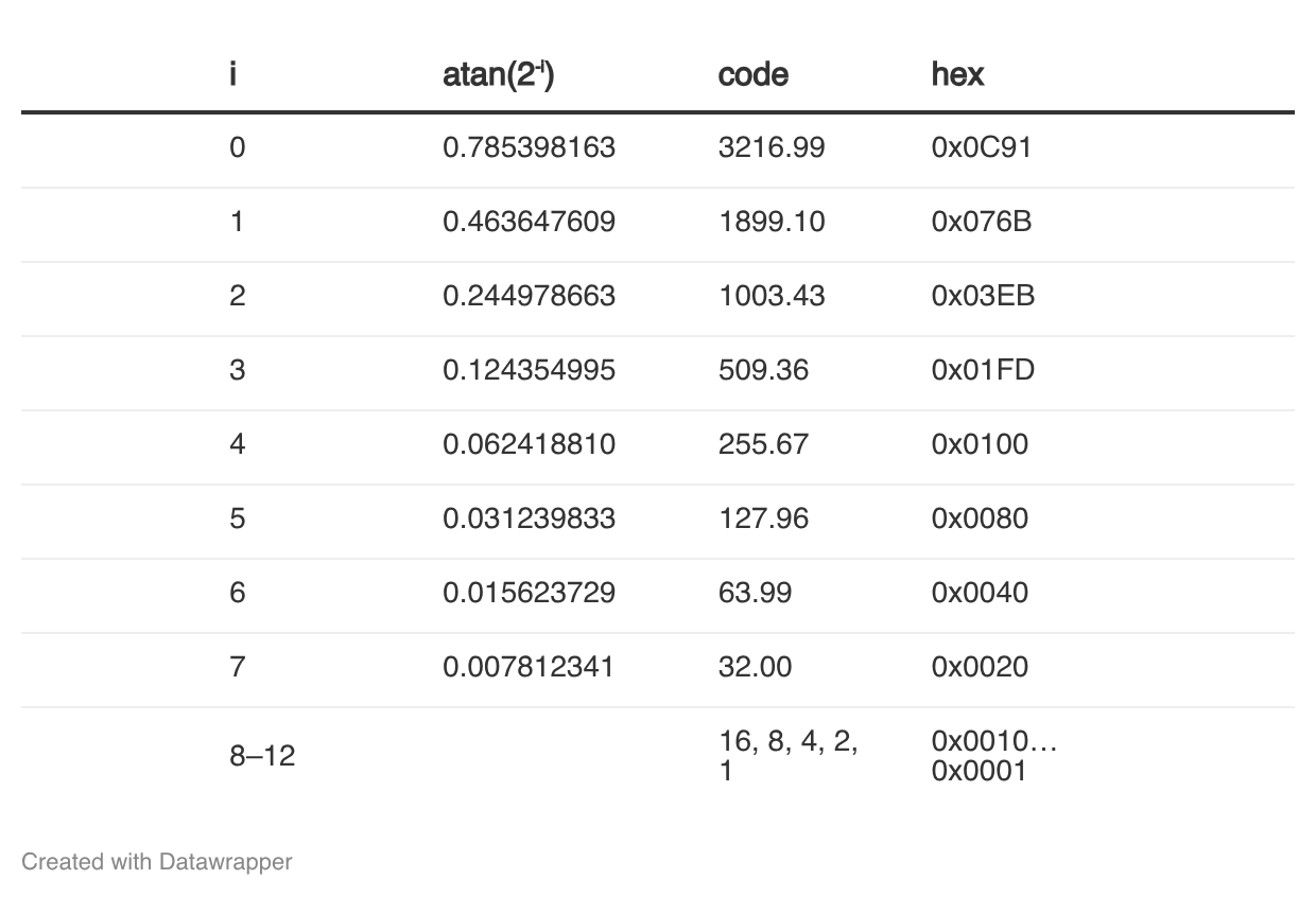
The important part is that we don’t need to store these numbers.
We can generate them.
That is the trick behind the ROM-less implementation.
Designing for a Tiny Tapeout
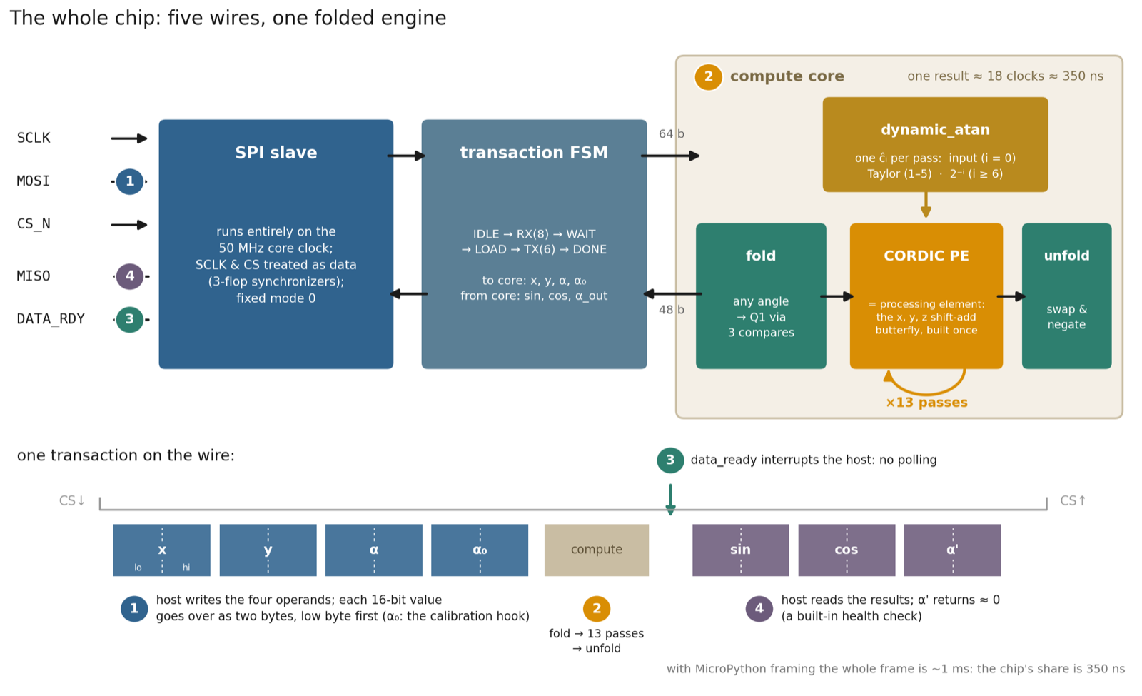
ROM-less implementation doesn’t have the table. What it has instead is four small Verilog modules behind five wires: an SPI slave, a transaction FSM, an angle generator, and a single CORDIC processing element that gets reused for every iteration.
Numbers are Q3.12 fixed point throughout, 12 fractional bits, 1 LSB = 1/4096 ≈ 2.44e-4.
The CORDIC uses signed fixed-point values with 12 fractional bits—effectively a Q3.12 representation.
The ASIC interface is deliberately minimal:
Inputs
- SCLK
- MOSI
- CS_N
Outputs
- MISO
- INTERRUPT
How RTL works
ROM-less CORDIC implementation with 16-bit signed fixed-point input Q3.16 (1 sign bit, 3 integer bits, and 12 fraction bits). This core comprises mainly (i) a single-stage CORDIC engine that operates in rotation mode for computing cos and sin of input angle θ, and (ii) an arctan generator that generates the micro-rotation angles dynamically in each clock cycle for the corresponding iteration.
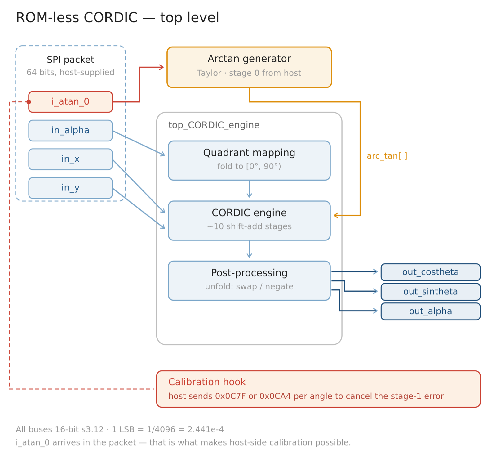
The host sends four 16-bit values to the design: atan_0, alpha, x, y and receives: alpha, cos(theta), sin(theta).
The core itself runs at 50 MHz.
The resulting layout occupies roughly: 334.88 µm × 225.76 µm, with 4042 standard cells, excluding fill and tap cells, and approximately 41.2% routing utilization. The design’s specified maximum clock frequency is 50 MHz.
For a mathematical accelerator that started life as an equation on a whiteboard, seeing an actual piece of silicon emerge from it is pretty cool.
But the real test was still ahead.
Angles generated, not stored
The angle generator, dynamic_atan, produces one coefficient per iteration in lockstep with the engine, and it treats the iterations in three regimes.
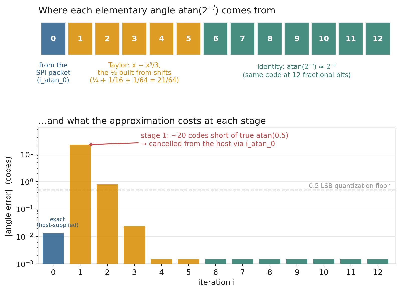
Iteration 0 doesn’t compute anything. atan(2⁰) = 45° is where a short Taylor series is at its worst, so the design sidesteps the problem entirely: the value arrives from outside, over SPI, as i_atan_0, packed into every transaction next to x, y and the target angle. At design time this was a convenience. Remember it; it turns out to be the whole story.
Iterations 1 through 5 use the two-term expansion atan(x) ≈ x − x³/3, and the 1/3 is itself built from shifts:
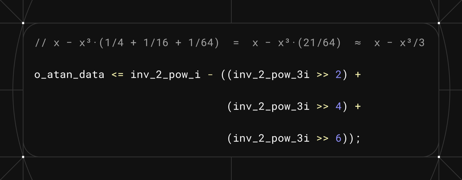
A geometric-series approximation of the coefficient, inside a Taylor approximation of the function. There is no multiplier anywhere in this chip.
From iteration 6 onward there’s no series at all, because at 12 fractional bits atan(2⁻ⁱ) and 2⁻ⁱ round to the same code. The generator just emits the shift. The design docs quantify what all this approximating costs: a MATLAB model over 1000 samples put the mean absolute output error at 0.003. Hold that number for later.
One engine, thirteen passes
This design instantiates the element once and iterates in place. The inner loop is three registered shift-adds:
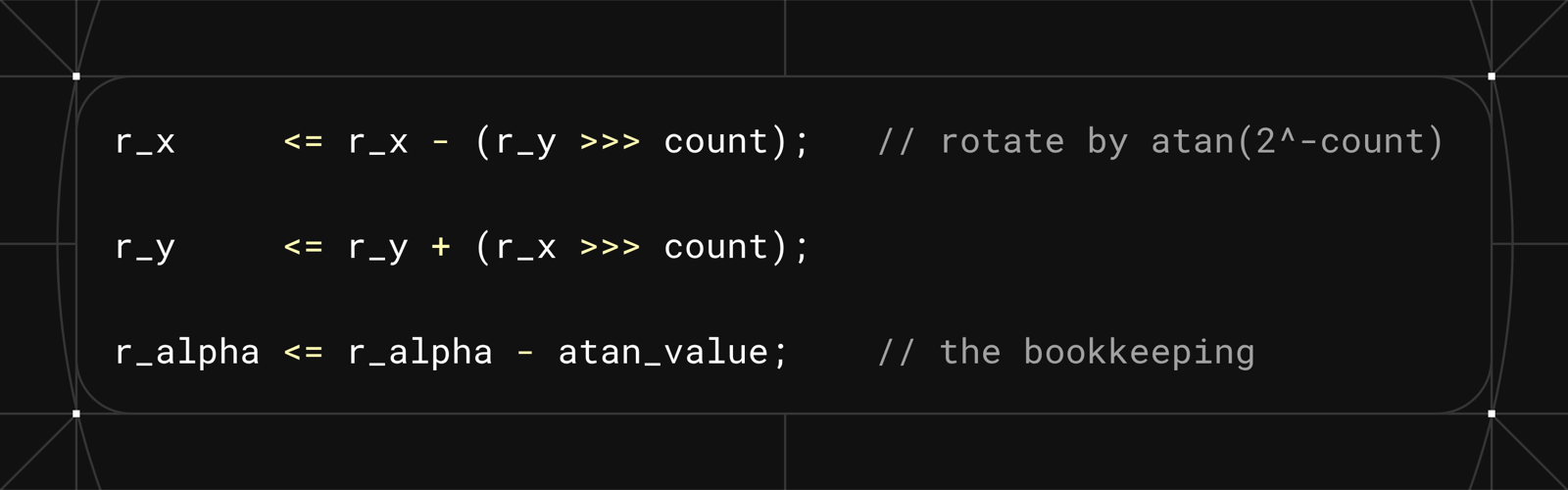
with all three signs flipping together when the direction bit says rotate the other way. A result costs the 13 iterations plus a few cycles of housekeeping, under twenty core clocks, roughly 350 ns at 50 MHz. On a 2×2 Tiny Tapeout tile the trade is obvious: latency is irrelevant next to the SPI transaction wrapping it, and area is what you actually pay for. Unrolling would multiply the datapath thirteen-fold to gain throughput that nothing downstream could use.
Folding the circle
A rotation CORDIC only converges within the sum of its elementary angles, which for this configuration is Σ atan(2⁻ⁱ) ≈ 99.9°. Feed it 200° and the angle accumulator saturates, the direction bits stop carrying information, and the output is garbage. Not gracefully degraded garbage, either. So the full circle gets folded into the first quadrant before the rotator sees it, and unfolded after.
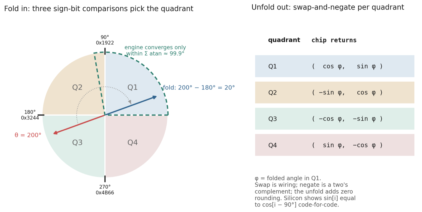
The fold costs three subtractions and some wiring. The input angle is compared against π/2, π and 3π/2 (0x1922, 0x3244, 0x4B66 in Q3.12) by checking the sign bits of the three differences. Two small boolean equations turn those sign bits into a 2-bit quadrant code, and the matching difference becomes the folded angle. On the way out, the quadrant code selects a swap-and-negate of the cos/sin pair: Q2 returns (−sin, cos), Q3 returns (−cos, −sin), Q4 returns (sin, −cos). Swapping is wiring and negation is a two’s complement, so the unfold introduces no rounding at all. Silicon later confirmed this directly: across a fine sweep, the sin output is the cos sequence displaced by exactly 90°, code for code.
Five wires and a byte protocol
The entire chip interface is SPI plus one interrupt: SCLK, MOSI and CS in, MISO and a data-ready line out. Five wires.
Below shows the four steps as they appear on the wire —
The SPI slave is deliberately boring, in the good way. Nothing inside the design runs on SCLK. The slave treats SCLK and CS as asynchronous data, passes each through a three-flop synchronizer clocked at the 50 MHz core clock, detects edges, and does all its shifting in the core domain:
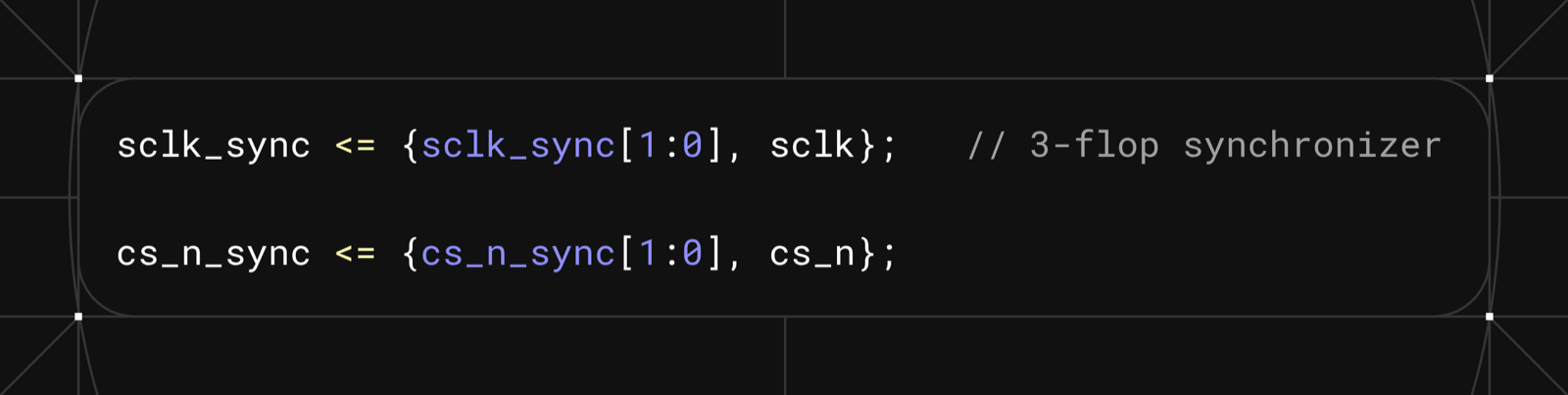
One clock domain, no gated clocks, no metastability windows, fixed SPI mode-0 behaviour. This is the textbook-safe way to build an SPI slave in an ASIC. Hold this for later.
On top of the slave sits a six-state transaction FSM: idle, receive, wait, load, transmit, done. Eight bytes in (x, y, angle, α₀, low byte first), then the engine runs, then the data-ready pin goes high so the host doesn’t have to poll, then six bytes clock back out: sin, cos, and the converged angle accumulator, which should come back near zero and doubles as a health check. CS going high resets the FSM for the next transaction.
From MATLAB to GDS
Verification before tape-out ran four rungs. A MATLAB model established the math and the 0.003 error budget. An Icarus/GTKWave testbench swept 999 angles from a stimulus file through the RTL and diffed the cos/sin outputs against golden values. The standard Tiny Tapeout cocotb bench ran the design at RTL and again at gate level after hardening. As said, micro-rotation angles were generated using Taylor’s series approximation; it is found that the mean absolute error between actual and computed value is 0.003 for 1000 samples.
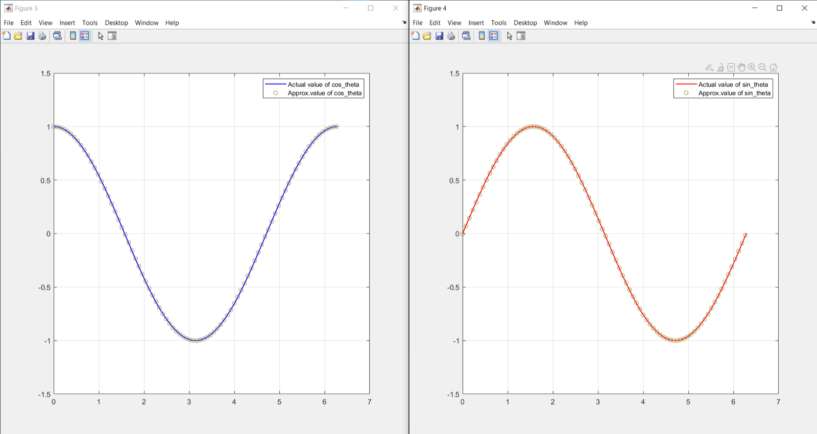
Then, before committing to a shuttle, the design went onto three FPGAs. A Digilent CMOD A7 (Artix-7), driven over Linux spidev. A ULX3S 85F (ECP5), built with a fully open yosys → nextpnr → ecppack flow, with a Pico as the SPI master at a gentle 20 kHz and timestamped regression JSONs committed to the repo. And Vaaman, Vicharak’s Efinix Trion T120 + RK3399 board, which is fitting given how much of the math and RTL came from their team. Same byte protocol, essentially the same Python regression script on all three. That script is the direct ancestor of the silicon harness in the rest of this post.
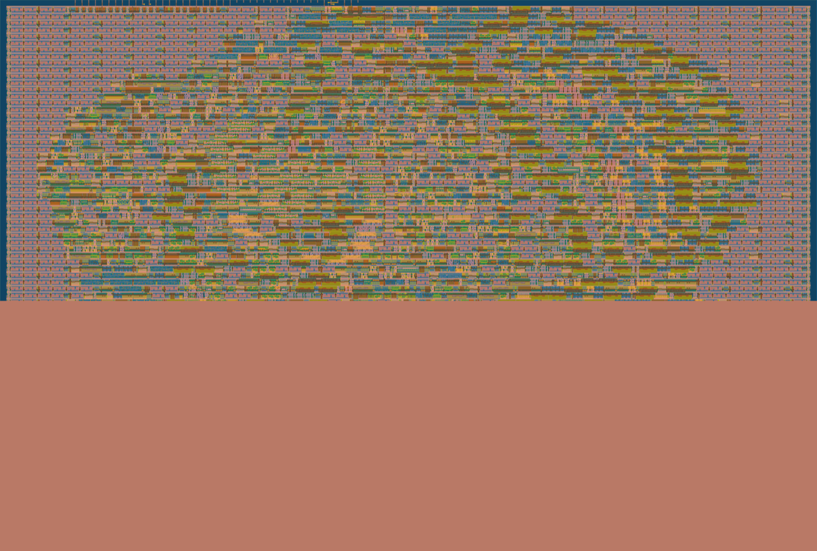
Hardening was the near-stock Tiny Tapeout OpenLane flow: 20 ns clock constraint, 60% placement density target, routing capped at met4. The result is a 2×2 tile, 334.88 × 225.76 µm, 4,042 standard cells, 41.2% routing utilization, closing timing at 50 MHz.
Don’t trust simulation
One of the things that became important after this project was separating three different questions:
- Does the mathematics work?
- Does the RTL work?
- Does the physical chip work?
They are not the same question. For silicon bring-up, we built a dedicated test harness around an RP2350. The host runs MicroPython and acts as the SPI master.
For every test angle, it:
- generates the input vector,
- sends the CORDIC transaction,
- waits for the data-ready interrupt,
- reads back sine and cosine,
- converts the fixed-point result,
- compares it against a double-precision software reference.
And then we sweep the angle. Not just five test vectors. A full sweep of 250 angles.
The harness repository contains the characterization scripts, measurement data, reports, plots, and logic-analyzer decoding tools.
First silicon: it works… but badly
The first characterization run was actually encouraging.
The chip worked. SPI interface worked (with SPI Master@4-6 MHz). CORDIC converged. The outputs looked like sine and cosine.
100/100 angles functionally passed the regression test in 0.746 seconds.
The baseline numbers were:
1
2
3
Mean absolute error : 3.292e-3
RMS error           : 3.553e-3
Peak error          : 5.741e-3
In Q3.12 terms, that is roughly:
1
2
3
Mean absolute error : 13.5 LSB
RMS                  : 14.6 LSB
Peak                 : 23.5 LSB
The quantization floor of a 12-bit fractional representation is only 0.5 LSB. We were sitting around 47× above the theoretical quantization floor.
Before calling that a defect, look back at the design section (Figure 10). The MATLAB model simulated the Taylor generation at 0.003 mean absolute error, and the silicon measured 0.00329. The chip was doing almost exactly what its own documentation said it would.
The real question was whether the SPI host could beat the documentation, and answering it starts with a change of coordinates, because raw error-vs-angle plots are where debugging goes to die.
Separate gain error from phase error
The first useful debugging step was to stop looking at “CORDIC error” as one number.
We reconstructed:
\[\text{magnitude} = \sqrt{\cos^2 + \sin^2}\]and
\[\text{phase} = \operatorname{atan2}(\sin, \cos)\]from each returned pair, and the mess separates into two independent defects. There’s a small constant gain bias, meaning that the output vectors are slightly too long:
1
2
Mean magnitude error : +1.69 LSB
Maximum              : +3.81 LSB
The resulting phase error can be expressed as:
\[\text{phase error} = \Phi - \theta = -\sum_i \sigma_i (\hat{c}_i - \text{atan}(2^{-i}))\]where $\hat{c}_i$ is the elementary angle the chip produces for that pass’s iteration index $i$. The hat is doing real work in the notation: $c_i = \text{atan}(2^{-i})$ is the true elementary angle, $\hat{c}_i$ is whatever the chip produces as its stand-in.
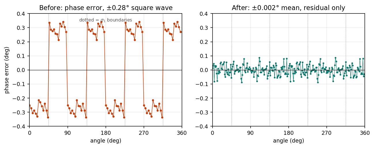
And there’s a much larger phase error of ±0.28° that is equal and opposite on either side of 45°: below 45° (mod 90) the phase reads −0.279°, above it +0.290°. A square wave, flipping at every 45° line—i.e. it changed sign around 45°, and then repeated every quadrant.
More interestingly, the phase error wasn’t random. It had a very obvious structure. That is a huge clue.
The error had a fingerprint
A CORDIC iteration makes a directional decision, the angle where its direction bit $\sigma_i$ changes sign:
\[\sigma_i \in \{-1, +1\}\]Stage 1’s boundary is 45°. Stage 2’s are 18.4° and 71.6°.
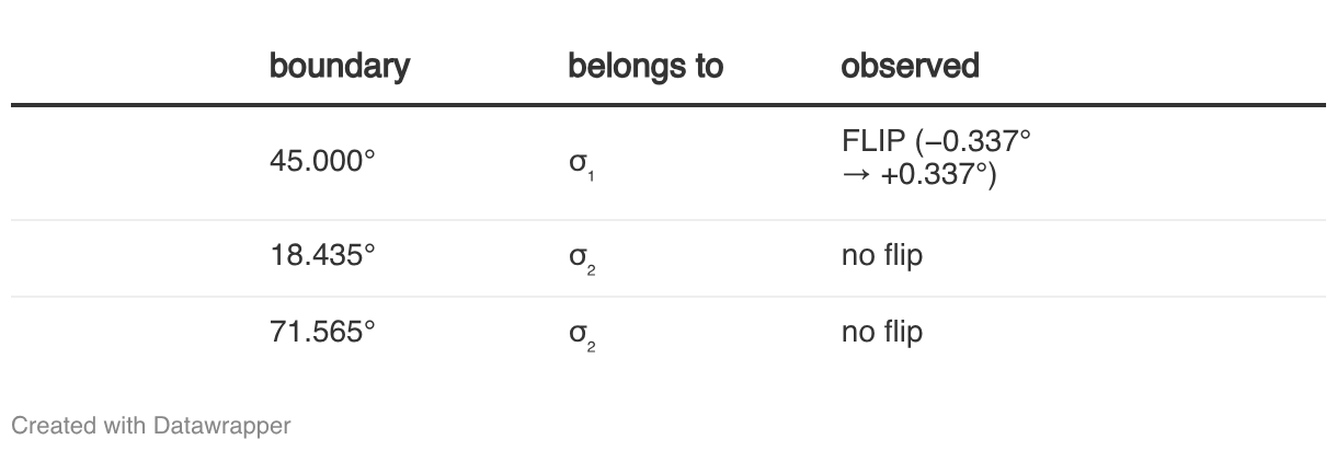
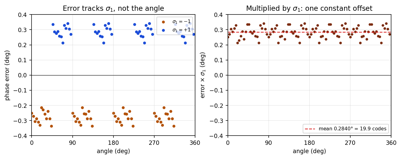
Only σ₁ flips where the error flips. Multiply the phase error by σ₁ sample by sample and the square wave collapses to a flat offset of +0.284° (about 20 codes).
So we asked:
What happens if we correlate the phase error with each iteration’s direction bit?
Regressing phase error against every stage’s direction bit at once achieved the breakthrough: σ₁ (first stage) carried +20.01 codes. Every other stage was comparatively tiny, under 2 codes and isn’t stable between runs (recall Figure 4).
The regression looked roughly like:
1
2
3
4
5
σ1 : +20.01 codes
σ2 :  +0.40
σ3 :  -1.83
σ4 :  -0.87
σ5 :  -1.06
The Fix and the subtle distinction
Here’s the distinction the whole fix rests on.
The rotation each stage physically performs is set by its shift amount. It rotates by exactly atan(2⁻ⁱ) whether the generated constant is right or not—that part is geometry.
As Figure 6 shows, the Taylor series feeds only the angle accumulator, the r_alpha register in the inner loop. So when the generated constant is short, the datapath still rotates correctly. The accumulator just records the wrong amount, and drives that wrong number to zero, which means it stops early. The vector ends up 0.28° from where the chip thinks it is.
The chip was never wrong about the rotation. It was wrong about what it had rotated.
The culprit: atan(0.5)
The first elementary angle was fine. Stage 0 arrives over SPI. It’s atan(1), and the exact Q3.12 code is:
1
3216.99 → 3217 = 0x0C91
which is correct to a hundredth of a code. That’s the whole reason it was made an input: the Taylor series is at its worst at x = 1, so rather than generate that value, the design takes it from the host. Stage 0 was never the problem.
At stage 1, x = 0.5, the two-term expansion produces code 1877 against the true atan(0.5) = 1899.1.
But the Taylor approximation used by the ROM-less generator was low.
A simple two-term approximation,
\[x - \frac{x^3}{3}\]at (x=0.5), produces approximately 1877 instead of 1899.
That’s a difference of roughly 22 codes. A 22-code deficit, matching the measured 19.9 in sign and nearly in magnitude.
Our measured phase bias? Approximately 20 codes.
Stage 2, at x = 0.25, is already within 0.011°, and the approximation improves roughly 30× per stage after that. From stage 4 down it’s bit-exact at this word length.
Stage 1 sits in the only gap: stage 0 is exact because it comes from the host, and stages 2 onward are small enough not to matter. Stage 1 is neither.
The silicon was telling us what the maths had already predicted.
The beauty of exposing the constants over SPI
There was one architectural decision that suddenly became extremely valuable: the first elementary angle was an input to the core.
The SPI transaction already carried atan_0. That meant the host could supply a calibrated value without changing the RTL.
Biggest takeaway:
Sometimes the best calibration mechanism is simply leaving yourself a parameter you can reach from outside the chip.
We then attacked the two main errors separately.
Fixing the gain
The CORDIC introduces a scale factor:
\[K = \prod_i \sqrt{1 + 2^{-2i}}\]For our configuration, the reciprocal scale factor is approximately:
\[1/K = 0.607252935\]In Q3.12: 0.607252935 × 4096 ≈ 2487.31
So the correct code is: 2487 = 0x09B7. The original value was one code too high: 0x09B8 → 0x09B7. That immediately moved the mean magnitude error from: +1.69 LSB to approximately: −0.54 LSB.
The calculation predicted about −0.51 LSB.
Measured silicon: −0.54 LSB.
That’s a very satisfying agreement.
Fixing phase without changing the chip
Now that we know the culprit is stage-1 angle. The stage-1 constant is generated inside the chip via the Taylor generator and cannot be changed. But its error enters the accumulator. We take that and multiply it by σ₁.
σ₁ is just which side of 45° the angle falls on, which the host knows before it sends the packet. So while stage 1 is out of reach, i_atan_0 is not. It arrives in every packet. Shifting it by the right amount, in the right direction for each half, cancels the stage-1 error exactly.
So the host sends a slightly different atan_0 depending on the angular half:
1
2
3
4
if degrees(angle) % 90 < 45:
    atan_0 = 0x0C7F
else:
    atan_0 = 0x0CA4
That is 3199, 3236 respectively.
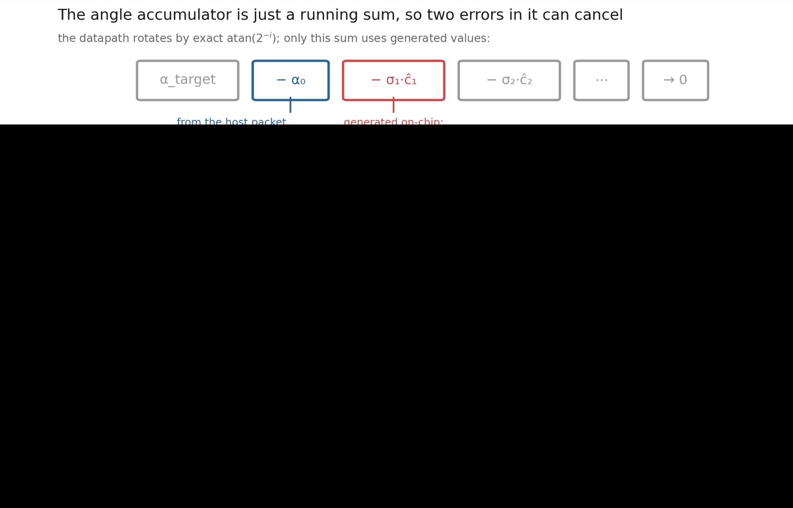
In other words, we effectively performed a host-side compensation for a deterministic silicon error:
The chip adds our wrong number to its wrong number and lands on the truth.
No RTL modification. No new mask. No submission to foundry again.
Just two different values in the SPI packet.
Then we made the test harder
A 100-point sweep was good enough to find the bug. It wasn’t good enough to characterize the final residual. So we went to 250 points.
The corrected design produced: 250 / 250 angles passed with 0 timeouts.
Final results:
1
2
3
4
5
6
Mean absolute error for cosine : 3.896e-4
Mean absolute error for sine   : 4.476e-4
Mean absolute error for overall: 4.186e-4
RMS error                      : 5.196e-4
Peak error                     : 1.352e-3
Maximum phase error            : 0.0872°
In terms of LSBs:
1
2
3
Mean absolute error : 1.71 LSB
RMS                  : 2.13 LSB
Peak                 : 5.54 LSB
The mean absolute error went from 13.5 LSB to 1.71 LSB. That’s a 7.9× improvement.
RMS improved by 6.8×. Maximum phase error dropped from approximately 0.343° to 0.087°. And about 66% of the final samples were within 2 LSB. The cardinal angles return cos 0° = 1.0002 and sin 0° = 0.0002, one code each. Worth restating against the design section: the MATLAB budget said 0.003, and calibrated silicon runs at 0.0004, roughly 8× better than the design’s own predicted accuracy, using nothing but the input the designers happened to route out.
All of it was independently confirmed from the wire: decoding the raw logic-analyzer capture with the host software removed from the loop gives a median error of 5.16e-4 against the host’s 5.20e-4 RMS, and a max of 1.340e-3 against 1.352e-3.
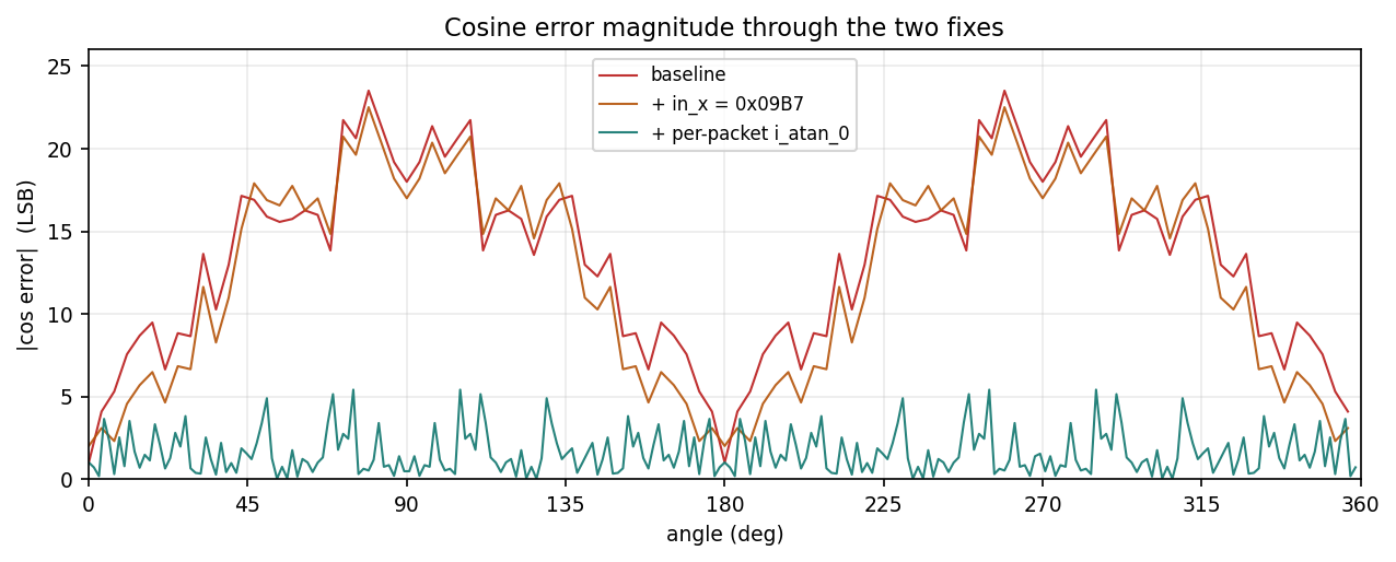
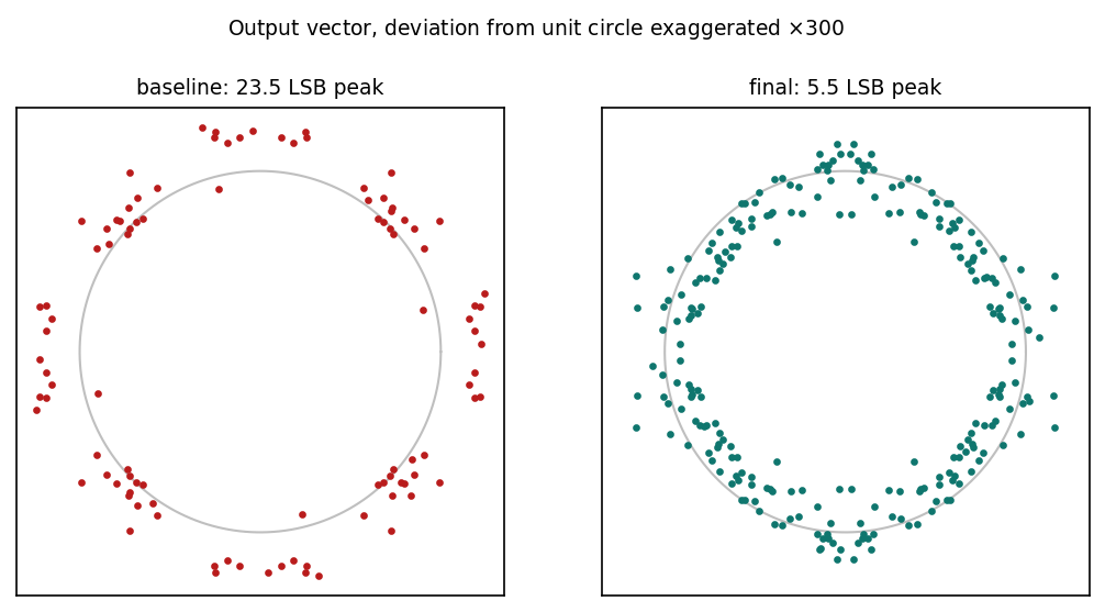
For a first silicon implementation of a ROM-less fixed-point CORDIC, that was a pretty good place to land.
But then the SPI started arguing with us.
The chip was right. We were reading it wrong.
At one point we tried pushing the SPI interface to 12 MHz with CORDIC system clock at 100 MHz.
The returned values suddenly looked suspicious. Everything was almost exactly half-scale. Not approximately half. Exactly half. That is a very specific failure mode.
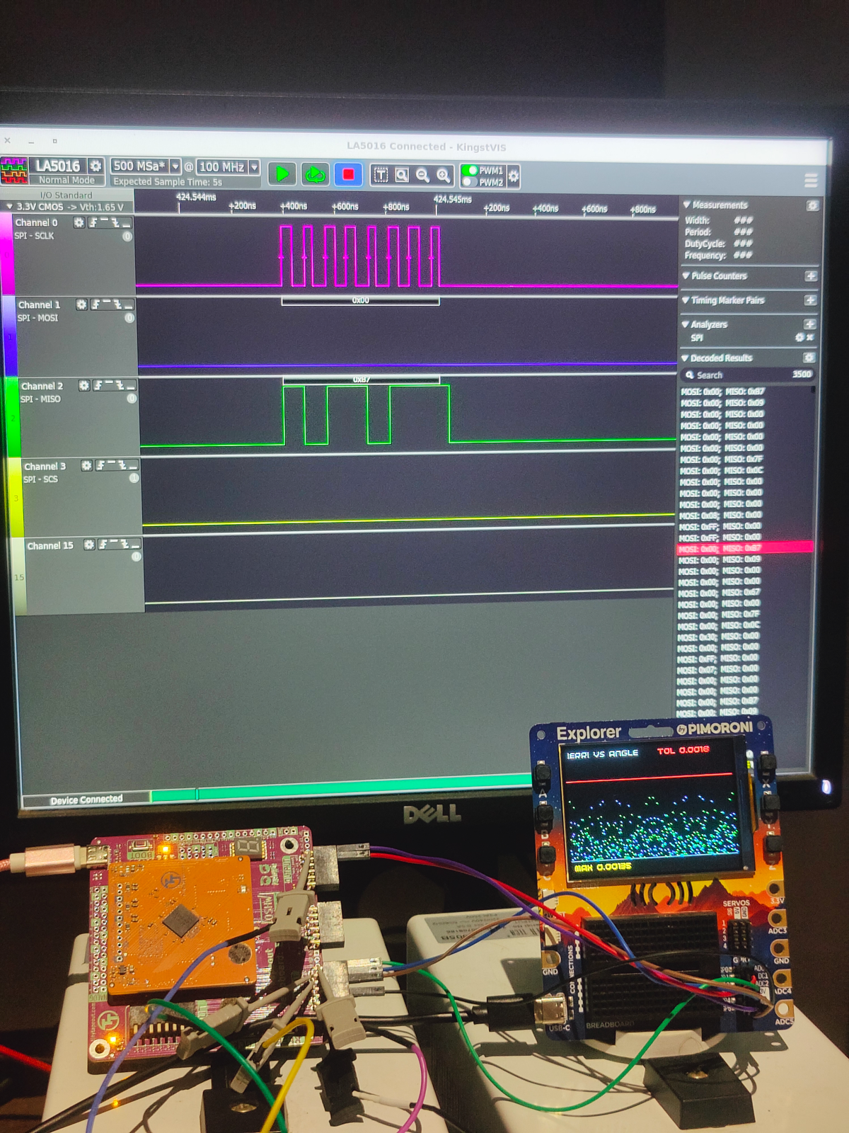
We captured the SPI bus using a logic analyzer.

And there it was. At 12 MHz with CPHA=0, the master was sampling the data one bit too early. The resulting magnitude was effectively divided by two.
The same wire capture, decoded on the correct edge, produced the correct values.
Decoded on the wrong edge:
1
cos(0°) = 0.50000
Decoded on the correct edge:
1
cos(0°) = 1.00024
The ratio was exactly:
1
0.500
across the samples. This wasn’t signal integrity or random corruption. It was a deterministic timing problem.
Why CPHA mattered
The CORDIC core is clocked at 100 MHz. The SPI clock is asynchronous to it.
The SPI input is synchronized internally:
1
2
3
sclk_sync <= {sclk_sync[1:0], sclk};
sclk_prev <= sclk_sync[2];
miso      <= tx_shift_reg[6];
So a change on SCLK doesn’t instantly cause MISO to change.
The logic analyzer measured MISO clock-to-out roughly ~50–60 ns.
That matched the RTL structure surprisingly well. At 100 MHz, one core clock is 10 ns. The synchronizer and edge-detection path therefore naturally introduce several cycles of latency.
The measurement showed roughly 4–5 core clocks from the SPI edge to the corresponding MISO transition.
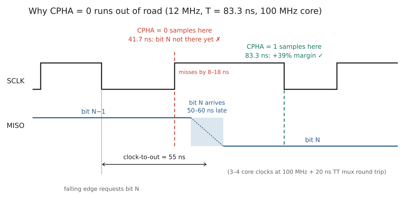
This is where having a real logic analyzer capture was incredibly useful.
We could stop arguing about what the RTL should do and simply look at what the silicon actually did.
The recommended SPI speed became 8 MHz
Although 12 MHz could sometimes appear to work, it wasn’t something we’d want to call qualified.
8 MHz was the sensible operating point.
And then we checked the wire independently
This part matters. It is very easy to build a test harness that accidentally proves itself correct.
The host software says the chip returned: 0.9987.
But how do we know the software actually decoded the SPI stream correctly?
So we decoded the raw logic-analyzer capture independently. The results matched.
The host-side analysis reported an RMS error of approximately: 5.20e-4.
The independent logic-analyzer decoding reported: 5.16e-4.
Maximum error:
1
2
Host : 1.352e-3
Wire : 1.340e-3
The MOSI stream was also decoded independently to verify that the calibration constants actually sent by the host were the ones we thought we were sending.
That gave us two independent paths to the same answer:
1
2
RP2350B host software → silicon → RP2350B host decoder
logic analyzer → raw bits → SPI soft decoder
When both agree, you can start trusting the result.
What I like most about this project
The CORDIC itself isn’t particularly exotic. CORDIC has been around for decades.
The interesting part, at least to me, was everything around it.
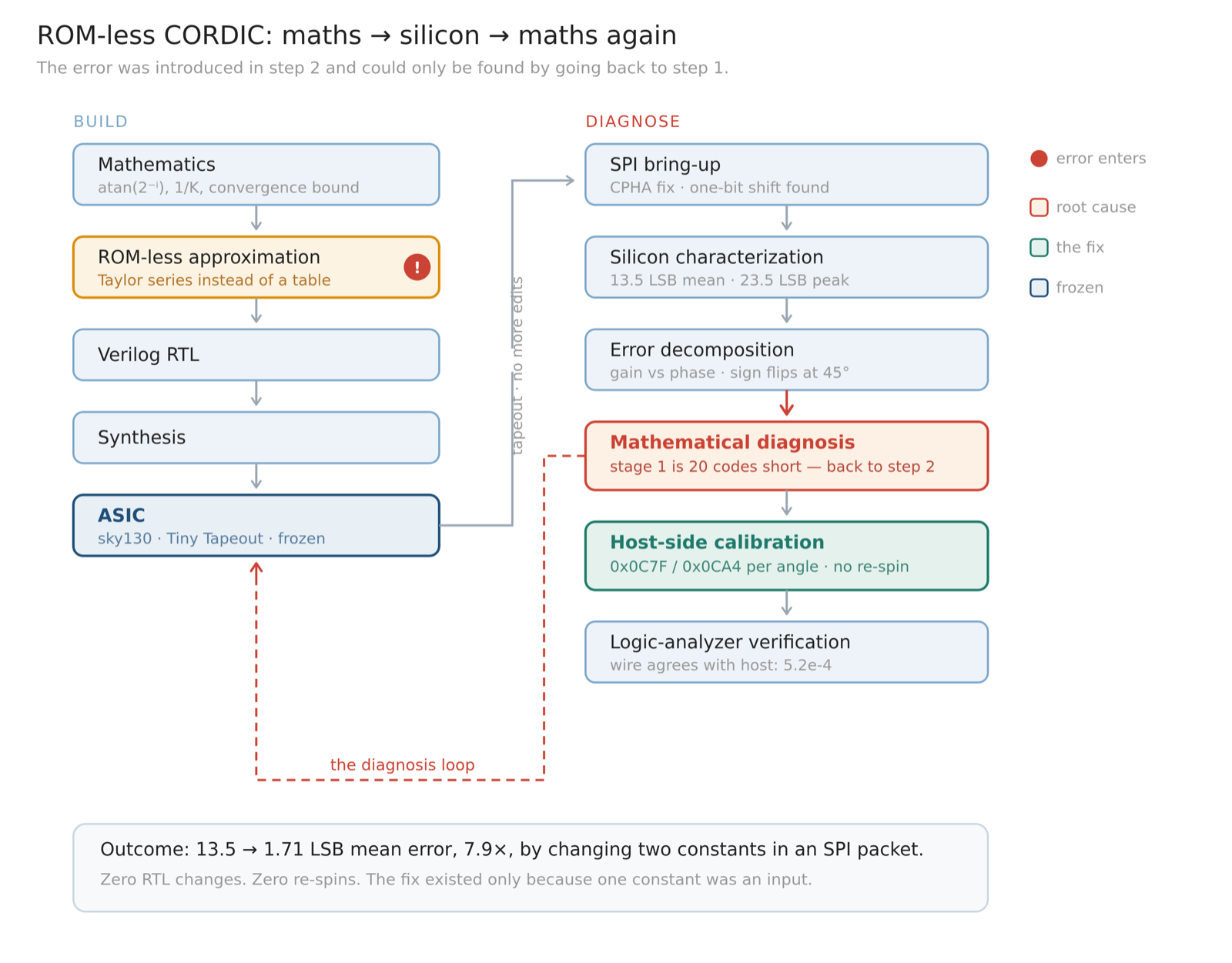
Each step exposed a different class of failure.
The simulation could tell us whether the RTL behaved as expected.
It couldn’t tell us whether our Taylor approximation was good enough at the actual fixed-point precision.
The silicon could tell us that.
The host could tell us the numerical error.
But it couldn’t prove that the SPI decoder itself wasn’t wrong.
The logic analyzer could tell us what physically happened on the pins.
And the mathematical regression could tell us why the error happened.
That’s the part of hardware engineering that is difficult to appreciate until you’ve actually done it.
A tiny ASIC teaches you a lot
The final design is small.
But the debugging wasn’t.
A 20-code phase error sounds trivial until you discover that it has a very recognizable structure.
A one-code scale-factor error sounds trivial until you can predict its effect to within 0.03 LSB.
An SPI timing problem sounds like a protocol bug until you discover that the wrong sampling edge produces exactly half the expected amplitude.
And a “working” testbench isn’t enough when the thing you’re testing is now sitting behind silicon, pads, synchronizers, clocks, and an actual physical wire.
That’s probably the biggest lesson we took away from this project:
ASIC debugging is less about finding the bug and more about finding measurements that make the bug impossible to hide.
The final numbers
The ROM-less CORDIC now runs with:
1
2
3
4
Process / platform : SKY130 / Tiny Tapeout
Core clock         : 50 MHz
Recommended SPI    : 8 MHz
Format             : signed Q3.12
Final characterization:
1
2
3
4
Mean absolute error : 1.71 LSB
RMS error           : 2.13 LSB
Peak error          : 5.54 LSB
Maximum phase error : 0.087°
And the most satisfying statistic:
1
250 / 250 tests passed.
No RTL modification. No new mask. No submission to foundry again.
Just a better understanding of what the silicon was actually doing.
The code
The complete RTL and Tiny Tapeout project are available here:
ROM-less CORDIC Engine — GitHub
The silicon characterization and RP2350 test harness are here:
CORDIC ROM-less V1 Test Harness — GitHub
The second repository also contains the characterization data, reports, plots and logic-analyzer decoding utilities used to reproduce the analysis.
Acknowledgements
This project was a team effort.
Rohan Sundar and I worked on the CORDIC architecture and the ROM-less mathematical approach, with Kasetty Praveen Kumar instrumental in designing RTL for the mathematics that made the ROM-less implementation practical.
The Vicharak engineering team contributed heavily to the RTL, verification and ASIC flow.
Devang Kabutarwala, Kasetty Praveen Kumar, Rishik Ram Jallarapu, Deepak Sharda, Tejas Dabhankar, Akshar Vastarpara
Rishik Ram Jallarapu contributed extensively to verification, GDS generation and gate-level simulation.
Kudos to them.
And of course, none of this would have made it through the tapeout process without the Tiny Tapeout community and the people who helped us navigate the practical realities of getting a real ASIC out the door.
第二部分:解析(深度解读)
以下为中文结构化解读,独立于英文原文,面向「半导体 / 数字 IC / 流片验证」读者。
一、核心论点摘要
这篇文章讲的不是「CORDIC 算法多巧妙」(那是 1959 年的老东西),而是一个更朴素的工程真理:硅回来之后,bug 是印在金属层里的;你能做的只有三件事——忍受它、花几个月重流片、或者留一道后门。作者团队在 Tiny Tapeout(SkyWater sky130 工艺)上流了一颗 无 ROM 的 CORDIC 引擎,首硅「能跑」,但平均误差比理论量化底噪高了约 47 倍。他们没有重流片,而是靠 SPI 包里两个常量 + 一个增益码修正,把均方根误差压低了 6.8×、平均绝对误差压低了 7.9×,250/250 个角度全过。
真正值得记的,不是修好了,而是修复之所以可能,完全是设计阶段一个看似随意的决定埋下的伏笔——把第一个微旋转角 atan_0 做成从外部 SPI 灌进来的输入,而不是在片内生成。
二、关键概念解读
1. 为什么是 CORDIC。 计算 sin/cos 通常不外乎乘法器、除法器或大 LUT。CORDIC 把旋转拆解成一连串「移位 + 加/减 + 比较剩余角度符号」的微旋转,每次转 atan(2⁻ⁱ)。它只需要一张查找表——各阶微旋转角。代价是迭代收敛慢,但对面积极度敏感的 Tiny Tapeout tile 来说,延迟无所谓、面积才是真金白银。
2. ROM-less 的核心思想。 微旋转角 atan(2⁻ⁱ) 随 i 增大而迅速「乖巧」:在 12 位小数精度(Q3.12,1 LSB ≈ 2.44e-4)下,从某一阶开始 atan(2⁻ⁱ) 和 2⁻ⁱ 量化到同一个码。于是作者把「查表」换成「用数学生成」:
- 第 0 阶(atan(1)=45°)泰勒级数最不准,直接由 SPI 输入
i_atan_0提供(设计的便利,后来成了命门); - 第 1–5 阶用两段泰勒 atan(x)≈x−x³/3,其中 1/3 也用移位实现,整颗芯片没有一个乘法器;
- 第 6 阶起连级数都不需要,直接发移位值。
整个数据通路就是「一个 CORDIC 处理元 + 迭代 13 次」,面积从展开 13 份降到 1 份。
3. 角度折叠(folding)。 旋转 CORDIC 只在 Σatan(2⁻ⁱ)≈99.9° 内收敛。喂 200° 会让累加器饱和、方向位失效、输出变垃圾。解法是在旋转前把整圆折进第一象限(与 π/2、π、3π/2 比符号位得 2-bit 象限码),旋转后再 swap-and-negate 展开。展开是纯布线 + 二进制补码取反,不引入任何舍入——硅上实测 sin 序列就是 cos 序列精确平移 90°。
4. SPI slave 的安全设计。 片内没有任何逻辑跑在 SCLK 上;SCLK/CS 当作异步数据,经 3-flop 同步器 打进 50 MHz 核心时钟域再做边沿检测,全移位在核心域完成。单时钟域、无门控时钟、无亚稳窗口、固定 SPI mode-0——这是 ASIC 里搭 SPI slave 的教科书式安全写法。一个六态事务 FSM(idle/receive/wait/load/transmit/done)吞 8 字节、跑引擎、拉 data-ready 中断、吐 6 字节,CS 拉高复位。
三、误差分解:把「一个数字」拆成「两个指纹」
首硅指标:平均绝对误差 13.5 LSB、RMS 14.6 LSB、峰值 23.5 LSB(量化底噪仅 0.5 LSB)。但原始误差-角度曲线是「调试者的坟场」——一眼看不出名堂。
作者的关键一步是换坐标系:从每个返回的 (cos, sin) 反算 magnitude = √(cos²+sin²) 和 phase = atan2(sin, cos),于是「CORDIC 误差」裂成两个独立缺陷:
- 一个很小的恒定增益偏置(向量略长,平均 +1.69 LSB);
- 一个大得多的相位误差,呈 ±0.28° 的方波,在 45° 处翻符号、每象限重复。
方波不是噪声——它是指纹。下一步是把相位误差逐样本乘以各阶方向位 σᵢ,做全阶回归,结果 σ₁ 独占 +20.01 码,其余各阶都 <2 码且不稳定。也就是说:误差只来自第 1 阶微旋转角生成得太低(x=0.5 时两段泰勒给出码 1877,而真值 atan(0.5)=1899.1,差约 22 码,与实测 20 码吻合)。
这里有个微妙但关键的区分:每阶物理旋转的角度由移位量决定,几何上永远精确转 atan(2⁻ⁱ);泰勒级数只喂给角度累加器 r_alpha。所以生成常量偏小时,数据通路旋转依然正确,只是累加器记了错的量、提前归零——向量停在「芯片以为自己转到的位置」差 0.28° 的地方。芯片从没搞错旋转,它只搞错自己转了多少。
四、修复机制:在 α₀ 注入等量反向误差
第 1 阶常量在片内由泰勒生成器固化、改不了;但它的误差进了累加器,再乘以 σ₁。而 σ₁ 不过是「角度落在 45° 哪一侧」,host 在发包前就知道。于是 i_atan_0 这个每包都到的输入就成了杠杆——按半八分象限给不同值:
1
2
3
4
if degrees(angle) % 90 < 45:
    atan_0 = 0x0C7F   # 3199
else:
    atan_0 = 0x0CA4   # 3236
旋转用精确角、累加器用生成角,而累加器是个求和——于是在 α₀ 输入端注入一个等量反向误差,账就平了。配合增益修正(1/K 的码从 0x09B8 改成 0x09B7,平均幅度误差 +1.69 → −0.54 LSB,与理论 −0.51 吻合),最终:
- 平均绝对误差 13.5 → 1.71 LSB(7.9×);
- RMS 改善 6.8×;
- 最大相位误差 0.343° → 0.087°;
- 约 66% 样本落在 2 LSB 内;
- MATLAB 预算说 0.003,标定后硅跑出 0.0004——比设计自己预测的好约 8×,且只用了设计者恰好引出去的那个输入。
原文金句:The chip adds our wrong number to its wrong number and lands on the truth.(芯片把我们的错数加到它的错数上,恰好落在真相。)
五、SPI 时序的那堂课:错一位 = 恰好减半
压测到 12 MHz(核心时钟 100 MHz)时,所有返回值恰好是正确值的一半——不是近似、是精确 0.5×。逻辑分析仪抓到:CPHA=0 时 master 在请求边沿后 41.7 ns 采样,而 bit 要 50–60 ns 才到(3-flop 同步器 + 边沿检测天然引入 4–5 个核心时钟延迟,100 MHz 下每周期 10 ns)。于是 master 早采了一位,幅度被整个除二。CPHA=1 等满周期则正确。结论:8 MHz 才是稳妥工作点,12 MHz 偶尔「看起来能跑」但绝不能算 qualified。
更漂亮的是独立验证纪律:用逻辑分析仪原始比特独立解码 SPI 流,绕开 host 软件,得到 RMS 5.16e-4 vs host 的 5.20e-4、峰值 1.340e-3 vs 1.352e-3;MOSI 流也独立解码确认发出的就是那两个标定常量。两条路径一致,结果才可信。
六、与本站其他文章的衔接
- SERDES / CPO 系列:本文的 SPI slave 设计(3-flop 同步、单时钟域、mode-0)正是高速串行链路里「跨时钟域安全」原则的微型版;而「错采样沿导致幅度减半」的教训,与 CPO/光互连里「可观测性决定你能不能定位失配」是一脉相承的。可延伸阅读 SerDes Part 1:CPO 之前你该知道的技术。
- 数值计算系列:「用泰勒级数+移位在硬件里生成 atan(2⁻ⁱ)」本质上是初等函数硬件化的一个特例,与 用单一算子生成全部初等函数 的思路互相映照——都体现了「数学近似 + 定点量化预算」这一核心工程权衡。
- 先进封装 / 测试插入:本文的「四道验证阶梯(MATLAB 模型 → RTL testbench → cocotb 门级 → 三块 FPGA → 硅上 RP2350 测试台)」正是质量保障从模型推向真实硅的范例,呼应 chiplet/2.5D 时代「测试插入点重定义」的主题。
七、风险提示与投资视角的边界
- 这是教学/个人流片项目,非商业产品:Tiny Tapeout sky130 shuttle、2×2 tile、334.88×225.76 µm、4042 标准单元、50 MHz——量级上是「证明一个想法能硅化」,不是量产 IP。其误差水平(1.71 LSB)对计算器/DDS 玩具足够,对高精度计量远不够。
- 「可校准性」才是真正的架构资产:文章最大的投资启示不是 CORDIC 本身,而是——把关键常量留一个片外可达的参数,等于把一次潜在重流片变成一次软件升级。对任何卖 IP/芯片的公司,这类「可观测、可标定」的设计哲学直接影响单位经济性与迭代速度。
- 原文无付费墙、全文已取得;所有配图已本地化(原图来自 substack-post-media S3 直链),不依赖外部 CDN,长期可读。
原始仓库:ROM-less CORDIC Engine | 测试台与标定数据