Enhancing SoC HW/SW Co-Verification with FPGA-Based Prototyping — 用 FPGA 原型验证打通 SoC 软硬协同
整理自 EDN:硬件辅助验证(HAV)已从「大型 SoC 才用得起」变成中端项目标配。传统软硬分离开发模式在速度与容量上双重失效,FPGA 原型验证才是打通软硬协同的关键路径——但工程难点不在 FPGA 本身,而在把现实世界的高速 I/O 灌进原型。Siemens EDA Veloce proFPGA CS 的扩展板方案是一次系统级回应。
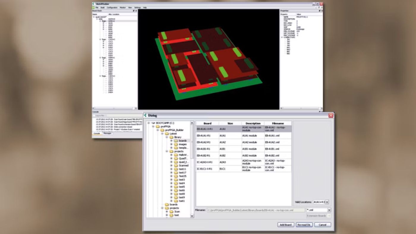
本文整理自 EDN(Electronic Design News)的技术评论文章,原文发布于 2026-09-01,作者 Juergen Jaeger(Siemens EDA prototyping 产品线总监)。结构为「正文(英文原文逐字转载)+ 解析(中文深度解读)」,方便中英对照阅读。
⚠️ 作者属于 EDA 厂商的产品负责人,本文对 Siemens EDA 的 Veloce proFPGA CS 方案有明显倾向;中文解读部分会补充三家主要 EDA 厂商(Synopsys / Cadence / Siemens)的横向对比作为平衡。
第一部分:正文(Original Article)
By Juergen Jaeger, director of prototyping product strategy at Siemens EDA — originally published on EDN, September 1, 2026.
The use of hardware assisted verification (HAV) technologies was once a luxury, “nice to have” technology for IC design. Because of the costs associated with HAV, especially for the “big box” logic emulators, it was mainly leveraged by the larger companies for their largest SoC projects.
Today with even medium complexity SoCs, modern HAV technologies have become far more accessible and affordable at a time when the use of HAV has become an imperative for helping design teams get massive SoC-powered products to market on time.
In today’s SoC design world, the issue isn’t strictly getting silicon to function properly. The main issue is ensuring that the SoC and the application software that runs on the SoC work together properly and with the highest efficiency.
Let’s examine a common methodology employed with verifying hardware and software together and where the traditional methodology breaks down. We’ll then look at how EDA vendors are offering modern FPGA-based prototyping systems in their HAV suites that bypass the shortcomings of the older methods.
The HW/SW, “chicken and egg” dilemma
On SoC projects, software development and testing can’t wait until silicon is available; on the other hand, embedded software development would need silicon to run on. As a result, design teams have come up with many techniques to make parallel development work. However, born out of necessity, one in particular has emerged over the years as the preferred methodology.
In this methodology, design teams attempt to separate the software stack into hardware-independent and hardware-dependent portions, separated by an operating-system layer and communicating through well-characterized APIs.
Typically, the larger hardware-independent code can be developed in a server environment with standard debugging techniques, using stubs to stand in for the APIs. Then the designers develop the hardware-dependent portion of the code, while the RTL design takes shape, using a hardware emulation system or perhaps even logic simulation as an execution environment.
But this methodology has its flaws. The first, and most obvious, is that it’s not always easy, or even possible, to determine which portions of the code are really hardware independent.
Dependencies accidentally created deep into the application code could go unnoticed, especially when intensive I/O and high computing loads must meet hard timing deadlines. And software developers often have to make some assumptions about execution speeds, cache sizes, and memory latencies—assumptions that may later prove false.
The second flaw of this older methodology is simply the combination of speed and capacity. In the older methodology, the integration and testing of the software with the RTL model of the chip is generally going to execute too slowly, even on an emulation system, to allow extensive exploration of the entire software stack. This leaves two options.
The first is waiting until first silicon is back and hope and pray all the bugs were caught; but hope is not a strategy and a software workaround or shut down part of the chip may not be feasible or acceptable. The second option is to move to a modern, success-oriented methodology that deals with shortcomings of the traditional hardware/software co-verification methodology.
This methodology is centered around hardware-assisted verification (HAV) solutions in general and FPGA-based prototyping in particular. Modern HAV technologies offer a much better methodology and higher likelihood of success that requires less stress and praying to a deity.
Addressing HW/SW co-verification bottlenecks
The end goal when deploying an HAV methodology is to ensure that not only is the SoC hardware functionally correct but that the software running on the SoC is optimized so the entire product meets spec and is optimized for best functionality, performance, and power. Ideally, the full software stack and the complete RTL design should be tested together as soon as both are sufficiently complete and stable to allow meaningful execution runs.
This gives the development team the opportunity to identify bugs and hardware/software interactions early, and before committing to silicon. And good version control ensures that the software team is working with the current RTL model and that the hardware team knows at once if they have just broken the software.
Speed of the HAV technology is the key. To test the full software stack on the SoC model realistically requires the use of an HAV technology, the FPGA-based prototype system. The model of the SoC under development is programmed onto the FPGAs of the prototyping system, allowing software developers to create software and run the software stack to ensure it works with the system.
An FPGA-based prototyping system will be able to run the full software stack on a realistic model of the SoC logic and memory, fast enough for intensive software and system validation. But what about the model’s interaction with the outside world? Verification requires seeing how the design behaves in continuous operation with real-world data.
In the past, many designs have attempted to circumvent the challenge of verifying their designs in continuous operations by trying to identify patterns of input data that will be most challenging to the system. They would synthesize those patterns as scripts and feed them into the prototyping system to observe its response. Unfortunately, this is ultimately a low-probability approach.
As years of development have illustrated, sometimes a bit too graphically, it’s just not possible to anticipate, for example, what streams of video from HD cameras are going to cause an AI system to miscategorize a traffic situation. And, as any communications engineer can attest, it’s equally impossible to predict the patterns of data that will appear on a real-world Gigabit Ethernet link or PCIe bus. As both ADAS and networking engineers have learned, a-priori analysis is no substitute for massive amounts of real-world data.
Ideally, verification engineers could connect the high-speed FPGA-based prototype directly to the cameras, sensors, actuators, and displays of the real system, and subject the system design to real-world data, in all its randomness, unpredictability, and at its natural speed. That could mean running the FPGA-based prototype system in a moving car, on a live network switch, or in a storage controller in a data center.
However, this raises another question: how to get at-speed or near-speed signals from the real world into the FPGA-based prototype. Design teams have tried several approaches, but once again, one solution is emerging.
Intuitively, it might seem reasonable to just implement the critical interfaces in the FPGA-based prototype. After all, the finished SoC will include those interfaces, so they are a real part of the design. And external networks, buses, and control signals could be connected directly into the prototyping system.
But there are serious issues with this approach. The first is that it will divert important design and verification resources away from the main design project. Yes, these interfaces will be present in the finished SoC, but they will almost certainly be implemented as third-party IP. Assuming that the third-party vendors have already been selected, they may or may not provide FPGA models of their IP for a particular FPGA family.
The models may or may not be accurate reproductions of the ASIC interface blocks’ functionality and will certainly differ in timing. Implementing these interface blocks in the FPGA and verifying them potentially becomes a significant FPGA design project in its own right, drawing on critical interface and FPGA skills that are needed elsewhere in the design.
An alternative is to design external interface adapter cards to connect the real-world signals into the prototype system. Such an adapter can run at full real-world speed on the real-world side, and at the speed required by the FPGA-based prototype on the prototype side. But again, there are significant challenges.
To begin with, no high-speed interface adapter is a trivial design, including power considerations, clocking, board design, connector or cable signal integrity, and so on. Then there is the matter of getting the signals back and forth between the adapter card and the prototype system.
Running cables to the system backplane will introduce timing and signal-integrity questions and will require precise understanding of the FPGA-based prototyping system’s internal design. Designing daughter cards to attach directly to expansion connectors or to the FPGA cards themselves within the prototyping system will require an even more detailed understanding of the system’s electrical, mechanical, and thermal requirements.
A modern solution
Take the case of a family of off-the-shelf extension boards for the Veloce proFPGA CS system. It includes I/O adapters for a range of interfaces, including Gigabit and slower Ethernet, PCIe GEN4, USB, DDR4, various Flash memory interfaces, and a range of connector configurations for bringing the FPGA I/O signals out of the box. Such an I/O board, for example, combines Ethernet on an RJ45 connector, a USB connector with UART, a MIPI 60 connector, and a GPIO header, along with user-definable LEDs.
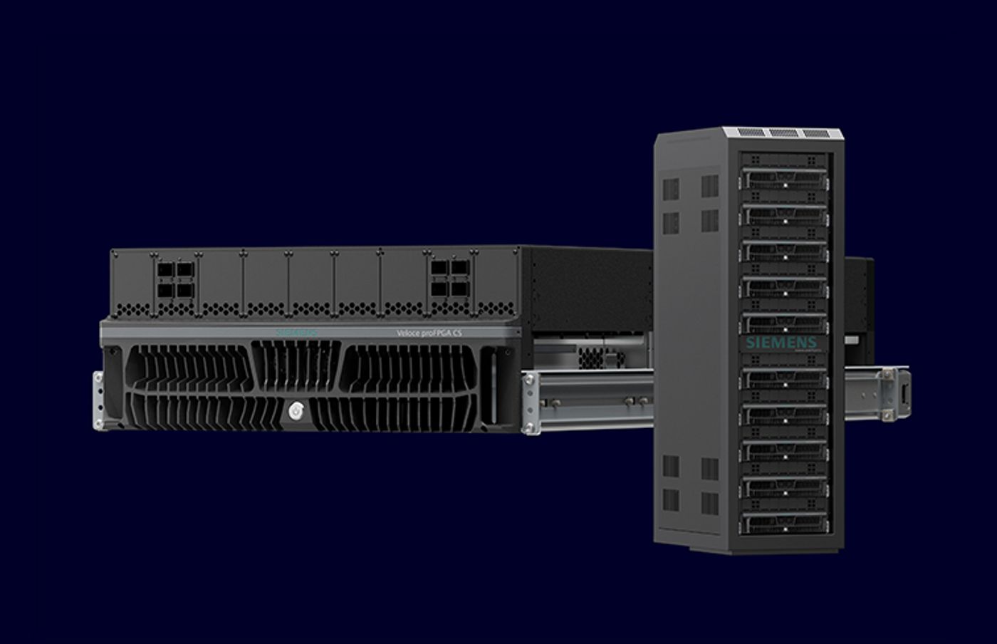
The extender cards plug directly onto connectors on the Veloce proFPGA CS FPGA boards, minimizing latency and signal-integrity issues. This also saves the user from having to provide external clock and power sources for the boards. Supporting software seamlessly integrates the extension boards into the Veloce proFPGA CS development environment.
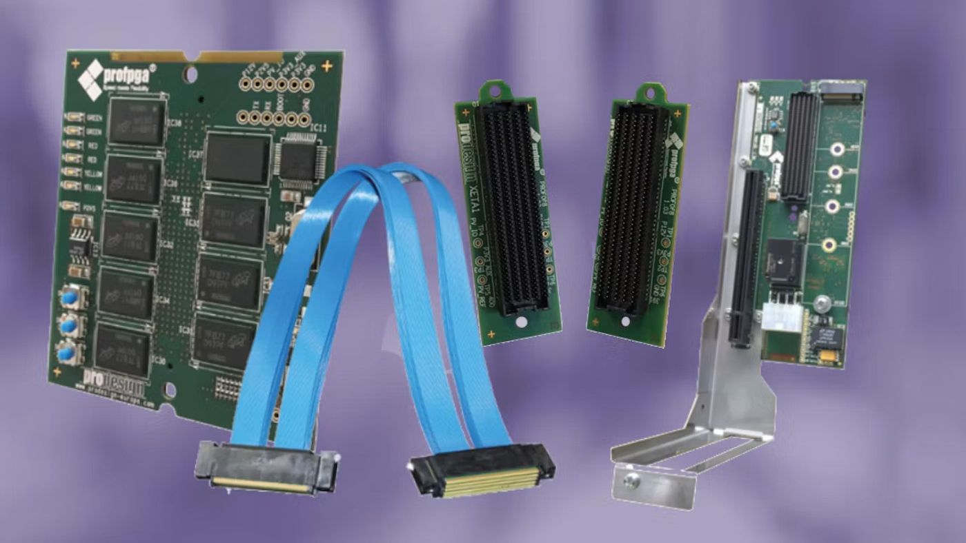
The result is that users can quickly connect an SoC prototype on the Veloce proFPGA CS into the actual environment in which the finished SoC will operate, with the interfaces operating at or near full speed. Software developers can instrument and observe the full software stack executing in the real world, not within the confines of synthetic tests. Hardware engineers can observe hardware/software interactions with live, real-world data at high speeds.
Juergen Jaeger is director of prototyping product strategy at Siemens EDA.
第二部分:解析(深度解读)
核心论点摘要
随着 SoC 复杂度飙升,硬件辅助验证(HAV)已从「大厂奢侈品」变成「中端 SoC 的必备项」。传统「软硬件分离开发 + RTL 在仿真器跑」的方法在速度与容量上双重失效——既看不清哪段代码真正依赖硬件,也无法在合理时间内跑完整软件栈。FPGA 原型验证才是打通软硬协同的「现代方法」:接近实时的运行、足够容量、价格可承受。但工程难点不在 FPGA 本身,而在把现实世界的高速 I/O 信号塞进原型。Siemens EDA 用现成的扩展板(Veloce proFPGA CS)系统性地回应了这个 I/O 适配问题。
关键概念解读
| 概念 | 含义 | 与本主题的关联 |
|---|---|---|
| HAV(Hardware-Assisted Verification) | 用专用硬件加速仿真,覆盖三类:ICE / Emulation / FPGA-based Prototyping | 速度、成本、容量成反比梯度;FPGA 原型验证是性价比甜点 |
| FPGA-based Prototyping | 用商用 FPGA 板搭多 FPGA 系统,把 RTL 编译后映射到板上运行 | 速度接近实时(MHz 级)、容量大(数亿门)、单价低(数万–数十万美元级) |
| 「Chicken and egg」困境 | 软件不能等硅片回来,硬件也不能等软件写完 | 倒逼软硬并行开发,FPGA 原型是最自然的并行平台 |
| Real-world I/O | 高速接口(PCIe Gen4/5、USB、Ethernet、MIPI、DDR4 等)的真实流量 | 是「能不能把原型接到真车上跑」的决定项 |
| 设计环境收敛 | 软件与硬件用同一份 RTL 不断同步迭代 | 好的版本控制 + 快速原型编译 = 团队减少「谁刚把谁弄坏了」的来回 |
传统方法为什么失败(作者的两条缺陷)
- 软硬件分离开发:分得清的部分(OS 以上的应用层)写起来快,但分不清的「深度依赖」容易埋雷——尤其是 I/O 密集、时序紧的代码段。开发期对 cache 大小、内存延迟、执行速度的假设经常事后被推翻。
- Emulator 跑 RTL 太慢:即便仿真器已能跑 RTL,速度也只到 MHz 量级,跑完整栈要数小时到数天。两条退路——「等第一颗硅回来边祈祷边 debug」或「换现代方法」——后者显然是工程上的唯一选项。
现代方法的真正工程难题:现实世界 I/O 接入
这是文章最有信息量的部分,也是中文解读应该重点展开的:
两种常见做法都不理想:
- 「把高速接口在 FPGA 里也实现一份」:SoC 里那些接口本来就来自第三方 IP,他们给的 FPGA 模型要么没有,要么时序对不上。在 FPGA 上重新搭一遍这些接口,会消耗关键的接口/FPGA 人才,且与主设计抢资源。
- 「自研 daughter card 转接」:每块板都要重做电源、时钟、信号完整性;走线延迟、电磁兼容、机械结构都要自己摸。是个独立的小项目,会拖慢主项目。
Siemens EDA 的回答——把第二种「自研转接」产品化:Veloce proFPGA CS 系统自带一套即插即用的扩展板,覆盖 Gigabit / 慢速 Ethernet、PCIe Gen4、USB、DDR4、各类 Flash、MIPI-60、GPIO、RJ45 接头、UART、各种 FPGA I/O 引出配置。板子直接卡在 FPGA 板上,没有线缆延迟,不需要外部时钟/电源。
三家 EDA 厂商横向对比(中文解读补充)
| 维度 | Siemens EDA Veloce proFPGA | Synopsys HAPS | Cadence Protium |
|---|---|---|---|
| 母公司 | Siemens(前 Mentor Graphics) | Synopsys | Cadence |
| FPGA 平台 | 自家多板堆叠(UNO 起步) | Xilinx / 自有 | Xilinx UltraScale |
| 上层仿真器 | Veloce(自研 ASIC 仿真器) | ZeBu(同源 ASIC 仿真器) | Palladium(同源 ASIC 仿真器) |
| I/O 扩展生态 | Veloce proFPGA CS 预制扩展板 | HAPS I/O 库 + 第三方 | Protium 适配 + Palladium 协同 |
| 卖点 | EDA 全栈整合(验证+原型+HLS+DFT) | 性能上限最高、定制最灵活 | 起步快、与仿真器协同流畅 |
| 价格带 | 中高端 | 高端 | 中端 |
| 适合场景 | 已有 Veloce 仿真器栈的 SoC 大厂 | 极致规模(>10 亿门)、极致速度 | 中等规模 + 想要一站式的团队 |
投资视角:Synopsys / Cadence / Siemens 三家在全球 EDA 合计 70%+ 份额(Synopsys ~35%、Cadence ~25%、Siemens EDA ~20% 含其它业务)。FPGA 原型验证是三家必争之地,但单做这点的中小厂(Aldec、S2C、Agilex/QuickLogic 等)依然在性价比赛道占据一片空间——尤其对预算紧、设计规模中等的项目。
技术趋势
- 「Pre-silicon hardware-software validation」成为新常态:单 SoC 软件栈复杂度爆炸(典型先进 SoC 含数千万–亿行代码,包括 OS、驱动、中间件、应用),跑全栈验证只能在原型/仿真器上做,传统边界用例测试已经不够。
- 「A-priori analysis is no substitute for massive amounts of real-world data」:验证哲学从「挑边界用例」转向「让原型接入真实流量」(视频流、PCIe 包流、传感器噪声),FPGA 原型天然契合,因为它的 I/O 带宽可达真实速率。
- 车规、边缘 AI、数据中心存储等场景的 SoC 越来越复杂,把「原型接真车 / 接真交换机 / 接真数据中心」这种「现场硅前验证」变成可能——这是 proFPGA 这类系统的核心商业逻辑。
- FPGA 容量与速度持续提升:Xilinx UltraScale+/Versal、Intel Stratix 10/Agilex 等新代际芯片让单板容量逼近数亿门,让「以前必须上 emulator 的项目」也能跑在原型上。
与本站其他文章的连接
- 之前发布过的 CPO 测试瓶颈 系列(PhotonCap 那篇)—— 同一系列关注「硅前测试」议题,但侧重点不同:CPO 那篇侧重晶圆级光学测试的物理时间瓶颈;本文侧重 SoC 功能 + 软件栈的硅前验证方法学。
- AI 硬件 / 高性能计算 类 SoC(NVIDIA 各类加速器、AMD Versal 自适应 SoC、Tenstorrent 等)的复杂度已远超传统 CPU/SoC,软硬协同验证的代价已成为 chipmaker 按时出货的关键变量。
- 中国 EDA 厂商(华大九天、概伦电子、广立微)目前在 FPGA 原型验证这条线尚处早期,跟进可关注其是否有「HES / HAPS 类对标」动作。
风险提示
- 作者立场:Juergen Jaeger 是 Siemens EDA 的 prototyping 产品线总监,文中的「Veloce proFPGA CS」案例解析部分必然含商业立场。具体技术参数(I/O 速率、容量、扩展板覆盖范围)可参考,但「现代 HAV 整体趋势」的论述是公允的——三大 EDA 厂商都在 FPGA 原型验证上重投入,方向上独立可证。
- 「与真车 / 真交换机对接」的代价:原理上 proFPGA 这类系统能做,但实际工程里仍然要求客户已有相对成熟的「目标系统」可接——对早期 SoC 反而用不上,反而是 emulation + FPGA 原型 + 仿真器三角组合更通用。
- FPGA 原型 vs Emulator 不是非此即彼:大型 SoC 经常是「emulator 早期软件栈 debug → FPGA 原型性能压测 + 真实 I/O 验证」的串联组合,单点选择会损失灵活度。