Architect Labs 发布 Redwood:号称全球首颗「完全由 AI 设计、并能跑 AI 模型」的 AI 芯片
Architect Labs 宣称其 AI 系统从人类规格说明出发,两周内端到端生成并完整验证了一颗可量产的 AI 加速器 Redwood,100% RTL/验证环境/固件/kernel 由 AI 产出,并给出对 Jetson Orin Nano 的 3.4× 每瓦性能投影。附中文深度解读与存疑点分析。
来源:Menlo Times — Architect Labs Unveils Redwood: The World’s First Fully AI-Designed AI Chip That Runs AI Models 原文链接:https://www.menlotimes.com/post/architect-labs-unveils-redwood-the-world-s-first-fully-ai-designed-ai-chip-that-runs-ai-models 原文发布日:2026-08-28 | 作者:Karan Bhatia(Menlo Times) 说明:本文为英文原文全文转载,附中文深度解读。解读部分为整理归纳,不代表原作者观点。
第一部分:正文(Original Article)
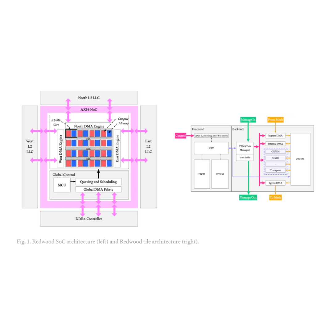 图01|Redwood AI 加速器(Architect Labs 官方配图)
Architect Labs, an AI research lab for custom silicon, led by Ebrahim Hussain and Aaditya Subedi, has announced that its AI System generated and fully verified end-to-end from a human-written specification, a production-worthy AI accelerator called Redwood.
With just two human architects providing the specifications, the AI system designed and fully verified the chip in under two weeks. It also co-designed the firmware and custom kernels and mapped modern AI models to the hardware. The resulting accelerator is currently running on an FPGA platform, performing inference on multi-billion-parameter models including Llama and Qwen.
Redwood represents a major milestone for the semiconductor industry: an AI system has autonomously designed a production-ready AI chip capable of running AI models. The approach creates a feedback loop between AI models and the hardware optimized to run them, potentially accelerating chip design beyond traditional development cycles.
Performance results also point beyond a proof of concept. Projected onto Samsung’s 8nm process, Redwood delivers 1.75× the throughput at 1.9× lower power than NVIDIA’s Jetson Orin Nano, translating to a 3.4× improvement in performance per watt on the same AI models.
Closing the Loop Between AI and Silicon.
Chip design can take years and hundreds of millions of dollars, while a shrinking pool of specialized talent has concentrated advanced semiconductor development among a handful of major companies. As a result, AI workloads are often adapted to hardware designed long before the latest models emerged.
Redwood takes a different approach by co-designing hardware and software from the start. Kernels, firmware, and RTL are developed and optimized together, allowing the chip to be tailored to AI workloads rather than forcing software to fit existing hardware.
This creates a continuous feedback loop in which improved AI models can inform better hardware designs, while more efficient hardware enables better AI performance, potentially accelerating both sides of the development cycle.
“Chips were designed by one or two engineers when I started in this business four decades ago. Since then, design complexity, time, and risk have grown exponentially. Even with every advance in EDA tools and technologies, a single chip program consumed multiple years and enormous engineering teams,” said Sunil Shenoy, former Senior Vice President of Engineering at Intel. “Redwood is a genuine paradigm shift, and a concrete benchmark of the frontier of what is possible. Architect Labs is democratizing capabilities that were the exclusive domain of a few giants, at a speed I would not have believed possible. Their approach promises to take hardware back to the future.”
Inside Redwood: A Frontier AI Accelerator.
Redwood is an end-to-end AI inference platform designed for physical AI applications such as robots, drones, and edge devices that require real-time performance within tight power constraints.
At its core is a scalable mesh of matrix and vector compute engines connected by a purpose-built on-chip network. The full AI inference pipeline, including attention, KV caching, and on-the-fly quantization, runs directly on the chip without relying on a host processor.
The compute engines, network, firmware, and custom kernels were designed together and optimized as a unified system, allowing the hardware to closely match modern AI workloads. Redwood can also scale into larger data-center SoCs or operate as a standalone chiplet.
**Key Statistics on Autonomous Redwood Design: **
- **Autonomous design and verification: **100% of the RTL, UVM verification environments, formal verification, firmware, drivers, and custom compute kernels were generated end-to-end by Architect Labs’ AI system from a human-written specification in under two weeks with two human architects working on the project.
- **Signoff-grade verification, zero hardware bugs: **Every block, from individual IP to the full SoC, closed at over 95% code and functional coverage using commercial EDA tools, Architect Labs’ proprietary formal engine, and hardware-in-the-loop validation. The first RTL drop from simulation to FPGA platform contained zero bugs.
- **Running real AI models on real hardware: **Redwood Nano is deployed on an AMD Versal FPGA at 250 MHz, executing real-time, single-batch inference on open-weight models including Qwen. Architect Labs ran live hardware demos at this year’s Design Automation Conference (DAC), one of the only companies at the show demonstrating an AI-designed accelerator running inference on models live.
- **Outperforming today’s leading-edge AI silicon: **Projected onto Samsung 8 nm, the same process class as NVIDIA’s Jetson Orin Nano, Redwood delivers 1.75x the throughput at 1.9x lower power, a 3.4x improvement in performance per watt, against a measured Jetson baseline running the same model. These projections are calibrated from direct FPGA measurements, not simulation alone.
- **Architectural iteration in days, not quarters: **Any change to the high-level specification results in fully regenerated, reverified, and redeployed hardware in under 48 hours, with the exception of SoC-level runs bounded by EDA tool runtimes.
- **Recursive self-improvement: **An AI model deployed on Redwood exposed as an API endpoint, discovered timing and kernel optimizations for the accelerator itself, at near-zero inference cost, closing the loop of AI and the silicon that fuels it.
“Every era of computing has been enabled by the underlying hardware, but also gated by who could afford to build the silicon for it,” said Steve Jang, Founder and Managing Partner at Kindred Ventures. “The Redwood chip is early proof that the gate can come down: two people - starting with a written specification and target AI model - used Architect Labs’ system to fully design, verify, and deploy a competitive AI accelerator in weeks. Whether you are a frontier research lab, robot maker, or a cloud operator, the concept of making your own custom silicon purpose-built for your product or platform is now becoming a reality.”
A Fundamentally New Way of Designing Software to Silicon.
Architect Labs’ AI system optimizes the entire computing stack, from models and kernels to firmware and RTL, in parallel, rather than through the sequential, siloed workflows common in traditional chip design. This allows software and silicon to be co-optimized through tape-out, with design iterations potentially taking weeks instead of months.
The approach can shift functions between software and hardware based on efficiency, for example, replacing thousands of software cycles with dedicated hardware logic or moving scheduling tasks to the compiler. Redwood demonstrates that these tradeoffs can now be designed, verified, and tested in hardware within days, providing a foundation for scaling the approach to more complex chips.
“Three decades ago, foundries like TSMC made world-class manufacturing available to anyone with a design, and the fabless industry with companies like NVIDIA, Broadcom, and Apple was born,” said Ebrahim Hussain, co-founder and CEO of Architect Labs. “In a similar fashion, we are pioneering the designless semiconductor industry, where chips like Redwood are co-designed and co-evolved with the workloads they run. We envision that software companies with intensive workloads or specialized AI models can get co-designed custom silicon, without having to build a large design team, stake a decade on an architectural bet, or fall back to off-the-shelf general-purpose solutions, leaving performance, power, and cost savings on the table. Every workload that matters deserves its own custom chip. We are building towards a future where they can have one.”
Architect Labs is already applying the same approach with Fortune 500 partners, co-designing custom chip designs at the speed of software and compressing programs that would traditionally run for months into ones measured in weeks. Redwood is the first public demonstration of what that makes possible.
第二部分:中文深度解读(Deep Dive)
解读声明:以下为基于原文的整理、归纳与延伸分析,不代表原作者或 Architect Labs 的观点。原文是一篇厂商发布稿性质的报道,解读部分会明确区分「原文主张」与「需要存疑之处」。
一、这件事到底宣称了什么
Architect Labs(由 Ebrahim Hussain 与 Aaditya Subedi 领衔)宣称:他们的AI 系统从一份「人类写下的规格说明」出发,端到端生成并完整验证了一颗可量产的 AI 加速器 Redwood。
按原文给出的 Key Statistics,具体的量化主张是:
| 维度 | 原文主张 |
|---|---|
| 人力投入 | 2 位人类架构师提供规格说明 |
| 周期 | 设计 + 完整验证,不到两周 |
| 生成范围 | 100% 的 RTL、UVM 验证环境、形式化验证、固件、驱动、自定义计算 kernel |
| 验证质量 | 从单 IP 到整 SoC,代码与功能覆盖率 均 >95%;首次 RTL drop 到 FPGA 零 bug |
| 实机运行 | Redwood Nano 部署在 AMD Versal FPGA @ 250MHz,实时单 batch 推理 Qwen 等开源权重模型;在 DAC 做过现场演示 |
| 性能(投影) | 投影到 Samsung 8nm(与 Jetson Orin Nano 同工艺档),吞吐 1.75×、功耗 1.9× 更低 → 每瓦性能 3.4× |
| 迭代速度 | 高层规格变更 → 重新生成、重新验证、重新部署 <48 小时 |
| 递归自改进 | 部署在 Redwood 上的模型(以 API endpoint 暴露)为加速器自身发现了时序与 kernel 优化,推理成本近乎为零 |
架构上,Redwood 是可扩展的矩阵 + 向量计算引擎 mesh,由专用片上网络(NoC)连接;完整推理管线(attention、KV cache、on-the-fly 量化)直接在芯片上跑,不依赖主机处理器。定位是 physical AI——机器人、无人机、边缘设备这类有实时性与功耗硬约束的场景。它既能扩成更大的数据中心 SoC,也能作为独立 chiplet 使用。
二、值得认真对待的三个信号
1. 真正的卖点是「设计周期压缩」,不是「性能超越」。 1.75× 吞吐、3.4× perf/W 这个数字容易被误读。它的价值不在「AI 设计的芯片比 NVIDIA 强」,而在「用 2 个人 2 周,做出了一颗能和成熟商用边缘方案同台比较的加速器」。如果这条曲线成立,改变的是芯片设计的经济学:过去一颗定制芯片要几年、几亿美元、几十人团队;如果这个数字降到「周级 + 个位数人力」,那么「为某个特定 workload 定制一颗芯片」就从「只有巨头能做的豪赌」变成「一家机器人公司也能考虑的常规选项」。
2. 软硬件「共同进化」是架构上的关键选择,而不仅是流程优化。 原文反复强调 kernels / firmware / RTL 是一起开发与优化的,而不是先定硬件再让软件适配。这正是当下 AI 芯片的核心张力——本站此前发布的《AI Chip Architectures》里有同样的观察:模型迭代速度远快于芯片设计周期,导致「AI workload 常常被适配到模型出现之前很久就设计好的硬件上」。Redwood 的做法是把这个错位反过来:让硬件围绕目标模型生成。那句「递归自我改进」(跑在 Redwood 上的模型反过来为 Redwood 找优化)是这个闭环最激进的表达——尽管它目前更像一个演示而非可持续机制。
3. 愿景的类比很精准:「designless(无设计)半导体产业」。 CEO Ebrahim Hussain 的类比是:三十年前 TSMC 这类代工厂把世界级制造能力开放给任何有设计的人,于是诞生了 NVIDIA、Broadcom、Apple 这样的 fabless 产业;现在他们想做的是把设计能力也开放出去。这个类比的力量在于它指出了产业分工的下一次解耦点——制造早已解耦,设计尚未。
三、必须存疑的地方(这点很重要)
原文的措辞相当强势,但报道体裁决定了它缺乏第三方核验。以下几个「限定语」在原文里都有,只是容易被 headline 盖过去:
- 性能是「投影」而非实测流片。原文明确写的是 projected onto Samsung’s 8nm process,且说明投影是「由 FPGA 实测标定,而非纯仿真」。这比纯仿真可信,但仍不等于 8nm 流片后的硅实测——功耗、时序收敛、SRAM/模拟宏单元的行为都可能与投影有偏差。
- 对比基线是 Jetson Orin Nano。这是 NVIDIA 的入门级边缘模组,不是旗舰。领先一个入门级边缘 SKU 是合理的阶段性成果,但不能外推为「AI 设计的芯片超越了最先进硅」。
- 「零硬件 bug」有明确作用域。原文说的是「首次 RTL drop 从仿真到 FPGA 平台零 bug」——即 RTL 到 FPGA 这一跳没出问题,而不是「量产 signoff 零缺陷」。这两者相差很远。
- 「100% AI 生成」与「>95% 覆盖」目前是厂商自述。覆盖率数字本身也值得玩味:形式化验证的价值取决于 property 写得好不好,而 property 是谁写的、写得多完备,原文没有交代。
- 验证仍然依赖商业 EDA 工具链。原文承认覆盖闭合用的是「商业 EDA 工具 + 自研形式化引擎 + 硬件在环验证」。这说明 AI 并没有取代 EDA 的签核(signoff)权威,而是把设计和验证的产出效率提上去了。
四、我的判断
如果把这些限定语放回原位,这条消息依然重要,只是重要性落在不同的位置:它不是「AI 造出了更强的芯片」,而是「AI 把芯片设计的固定成本打下来了一个数量级」。
对产业的潜在影响是:
- 长尾定制硅成为可能——机器人公司、垂直 SaaS、特定推理负载的云厂商,过去只能买通用芯片,未来可能负担得起一颗为自己 workload 定制的 chiplet。
- 迭代节奏从「代际」变成「周级」——规格变更 48 小时闭环,意味着硬件可以跟着模型一起演进,而不是每 18 个月赌一次架构。
- EDA 厂商的位置未必被削弱——至少在可见范围内,AI 设计仍需商业工具做签核背书;被冲击的更可能是「人力密集的前端设计与验证服务」这一层。
但这一切的前提是:从 FPGA 演示走到真正的量产流片。目前公开证据仍停留在 FPGA 平台 + 工艺投影。这一步的跨越幅度,历史上从不温和。
关联阅读(本站)
- AI 芯片架构全景:从 NVIDIA GPU 到 Cerebras 晶圆引擎与 Groq LPU —— 理解 Redwood 所声称的「软硬件协同设计」为何是当下 AI 芯片的核心张力,以及 decode 阶段为何是边缘推理的主战场。