XCENA MX1 CXL 计算型内存设备 @ Hot Chips 2026 — 与三星共推机架级「内存计算」
ServeTheHome 现场报道 XCENA MX1:一颗 Type 3 CXL 器件把 CXL 内存扩展、SSD 级字节寻址内存与 3072 个 RISC-V 近内存核熔于一炉,三星进一步给出机架级 CXL 内存池与 PNM 加速方案。
来源:ServeTheHome — XCENA MX1 CXL Computational Memory Device at Hot Chips 2026 with Samsung 原文链接:https://www.servethehome.com/xcena-mx1-cxl-computational-memory-device-at-hot-chips-2026/ 原文发布日:2026-08-25 | 作者:Patrick Kennedy(ServeTheHome) 说明:本文为英文原文全文转载,附中文深度解读。解读部分为整理归纳,不代表原作者观点。
第一部分:正文(Original Article)
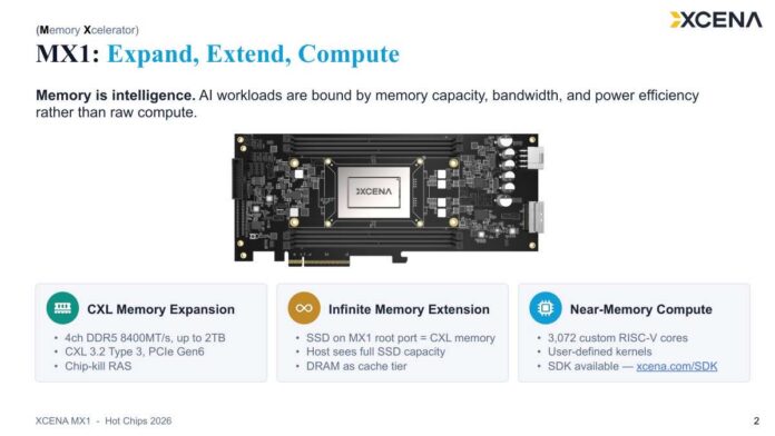 图01|Slide 2: (Memory Xcelerator)
XCENA is presenting its MX1 CXL computational memory device at Hot Chips 2026 in a joint session with Samsung that pairs the device with a rack-scale CXL memory plan. The XCENA MX1 is a Type 3 CXL part that fuses three ideas in one package: CXL memory expansion, SSD-backed storage presented as byte-addressable CXL memory, and near-memory processing across thousands of RISC-V cores. We covered the first generation of MX1 when it appeared as a CXL 3.0 computational memory part, and this session extends that story into rack-scale systems. We are covering this talk live, so please excuse typos.
XCENA MX1 CXL Computational Memory Device at Hot Chips 2026
XCENA’s core pitch is that AI workloads stall on memory capacity, bandwidth, and power efficiency before they stall on raw compute. CXL memory expansion spans four DDR5-8400 channels, reaching up to 2TB. Then there is an SSD on the MX1 root port exposed as CXL memory that the host sees in full. Finally, there is near-memory compute across 3,072 custom RISC-V cores. This is so cool.
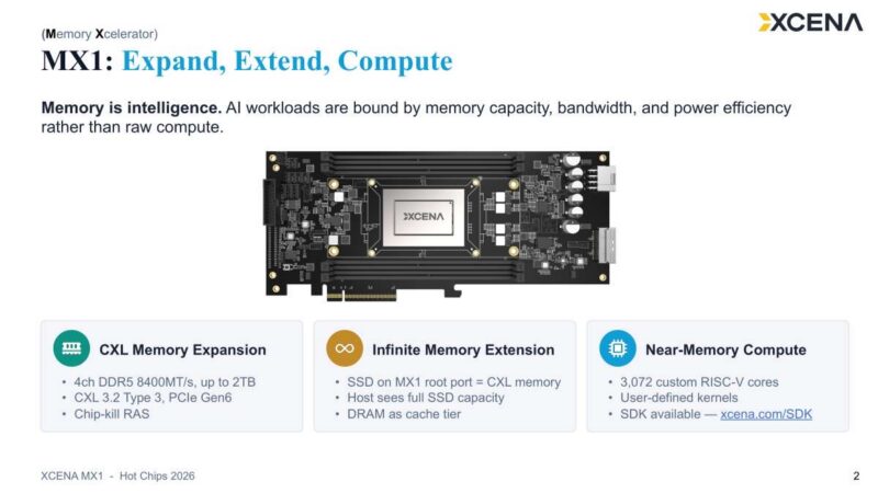 图02|Slide 2: (Memory Xcelerator)
XCENA built MX1 on Samsung Foundry’s 4nm process and organized the die into 24 subsystems, each composed of four clusters of 32 memory units, for a total of 3,072 MUs. XCENA describes the subsystem as the unit of host job allocation, with each subsystem able to run an independent job and share a 128MB L3 cache.
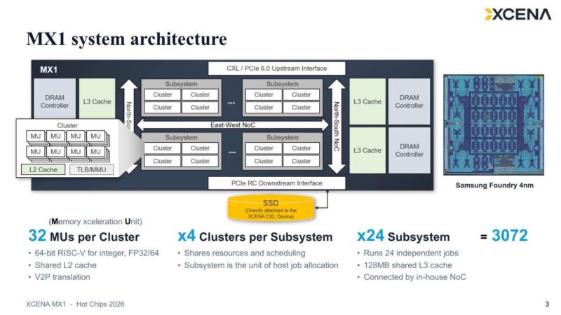 图03|Slide 3: MX1 system architecture
XCENA chose many simple in-order RISC-V cores over fewer large cores because the target workloads are bandwidth-bound and power-sensitive, and the smaller cores let the company fit 3,072 of them on the die while keeping energy per byte low. An open ISA also provides a mature toolchain and room for custom instructions for data-parallel work, such as in-memory analytics, RAG retrieval, and memory compression.
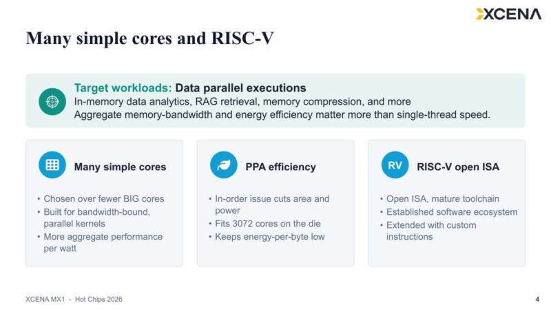 图04|Slide 4: Many simple cores and RISC-V
A Vector Processing Engine adds a vector path on top of the scalar MUs. XCENA delivers roughly 3 TFLOPS of peak dot-product throughput per MX1 SoC, with operations such as element-wise arithmetic, reductions, CRC32, and vector-scalar work, and per-MU command queues aimed at RAG vector search and KV cache scoring.
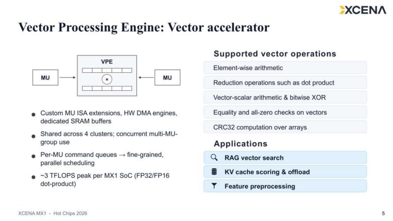 图05|Slide 5: Vector Processing Engine: Vector accelerator
Locality matters inside the chip. Each cluster shares an 8KB L1 instruction cache among four MUs and a 256KB L2 data cache among its 32 MUs, while a 128MB shared LLC ties the clusters together. Instructions use physical addresses while data uses host virtual addresses, with translation shared at the cluster.
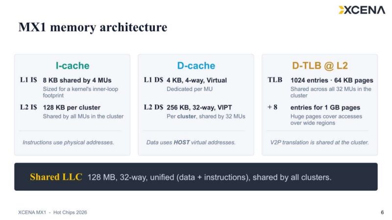 图06|Slide 6: MX1 memory architecture
One of the more important software decisions is whether to use a single virtual address space shared by the host and the MUs. Host and device see the same pointers, so pointer-rich structures traverse safely, and existing malloc-based code can move to CXL memory with minimal change, while a CXL-aware allocator keeps per-tenant page tables that isolate one app’s kernels from another’s memory.
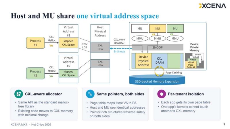 图07|Slide 7: Host and MU share one virtual address space
On the software side, XCENA ships a MapReduce-style runtime called PXL (the Parallel Xceleration Library). PXL walks an application from device context through kernel definition in C/C++ or Rust, jobs that allocate one or more subsystems, and a map API that splits work across MU cores with allocation and sync handled automatically.
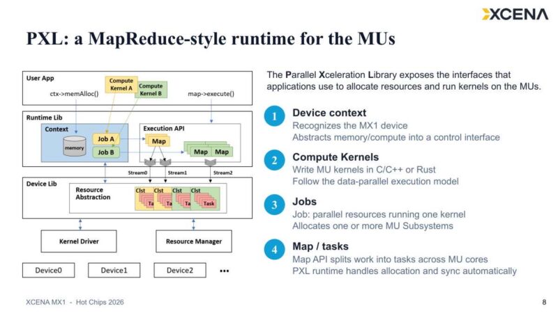 图08|Slide 8: PXL: a MapReduce-style runtime for the MUs
XCENA reports throughput up to 4.7x versus host-over-CXL and 2x versus local DRAM, at roughly a quarter of host power, resulting in efficiency gains of up to 18.7x versus CXL and 6.2x versus DRAM. XCENA ran the comparison on an Intel Xeon 6767P reference, excluding idle power.
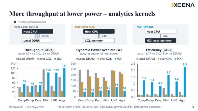 图09|Slide 9: More throughput at lower power - analytics kernels
Beyond DRAM, MX1 presents SSD capacity as byte-addressable CXL memory via what XCENA calls Infinite Memory, using a DRAM-plus-NAND hybrid in which DRAM caches SSD pages. This SSD is split into 64KB pages, tracked by a 1024-entry map cache TLB. Misses are filled by firmware running on the MU cores. I actually asked XCENA at FMS 2026 about this on the show floor. It is basically a memory tiering solution we have seen a few times over the years, with XCENA’s spin on it. If you are wondering, this is probably a good point in the presentation to bemoan the death of Optane.
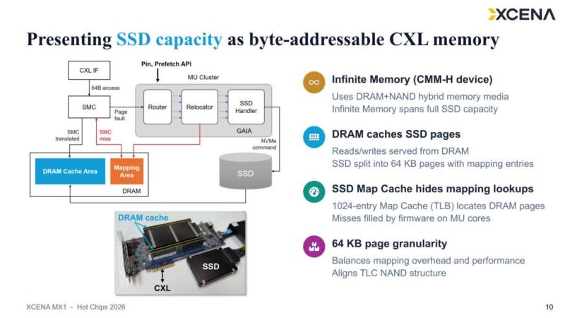 图10|Slide 10: Presenting SSD capacity as byte-addressable CXL memory
Infinite Memory ties directly into the KV cache story. With a pinned prefix that stays resident, XCENA shows query TTFT tracking DRAM at a modest 1.13x, while dropping the pin raises that to 1.57x and a raw SSD baseline to 1.86x. A lookahead prefetch that exploits device underutilization delivers nearly DRAM-resident performance. That test runs Llama-3.1-8B with vLLM, LMCache, and an NVIDIA RTX 6000 Pro. This is a really neat use case to me.
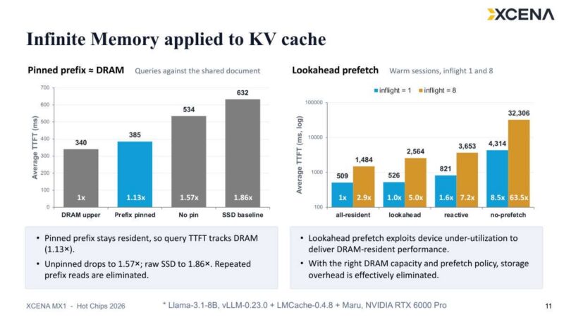 图11|Slide 11: Infinite Memory applied to KV cache
This second half of the session shifts to Samsung’s processing-near-memory research using MX1. Samsung’s analysis centers on using the large DRAM bandwidth behind the CXL interconnect by computing in place and moving only reduced data, with the figure contrasting DDR5 bandwidth at 268.8GB/s against a 64GB/s PCIe Gen6 x8 host link. Maybe the Gen6 x8 link gives away the timing of this since we are just starting to see Gen6 server CPUs launch. Samsung just said on stage that CXL is being adopted by all the major hyperscalers for things like databases and AI/ KV cache.
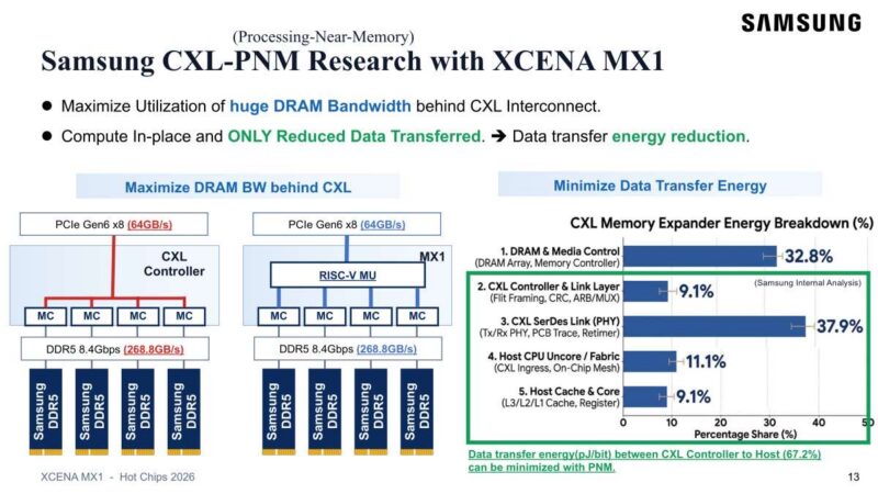 图12|Slide 13: (Processing-Near-Memory)
Samsung and XCENA sketch a rack-scale CXL computational memory system in which GPU servers share memory through CXL memory semantics. This reference appliance pairs a Liqid CXL switch with GPU servers using 96GB NVIDIA RTX Pro 6000 Blackwell parts and targets 20TB of memory capacity at 2.7TB/s of bandwidth.
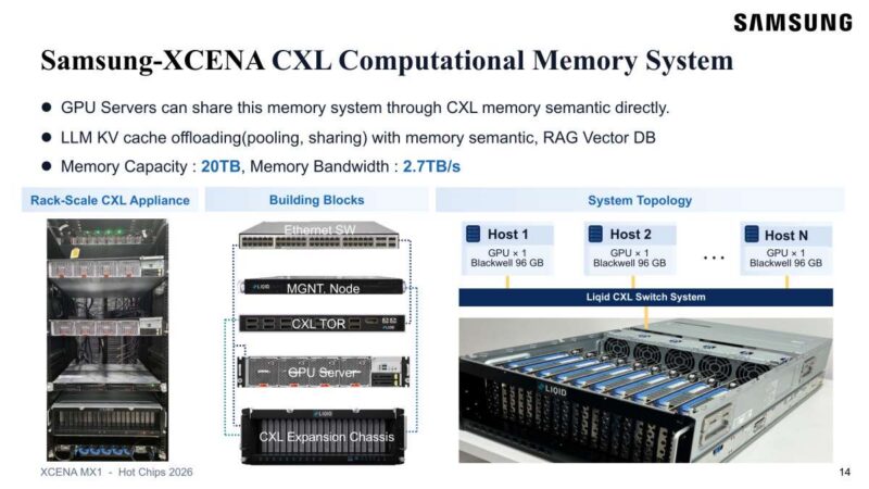 图13|Slide 14: Samsung-XCENA CXL Computational Memory System
Samsung brings the NDC API, a near-data-computing library it describes as vendor-agnostic and open-sourced through OCP FTI DCC. Samsung routes PyTorch integration through OpenXLA and PrivateUse1, so an AI framework can reach the XCENA PXL library without code changes.
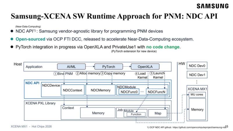 图14|Slide 15: Samsung-XCENA SW Runtime Approach for PNM: NDC API
Samsung’s first AI use case is RAG vector search on CXL-PNM using IVF Flat indexing from FAISS, with the L2 kNN distance computation offloaded because it is memory-bandwidth-bound. Samsung reports 10 PNM devices delivering 64x higher queries per second than a host CPU with a CXL memory pool, and 65x better query-per-energy, built on a 512M-vector FAISS index drawn from Laion 5B.
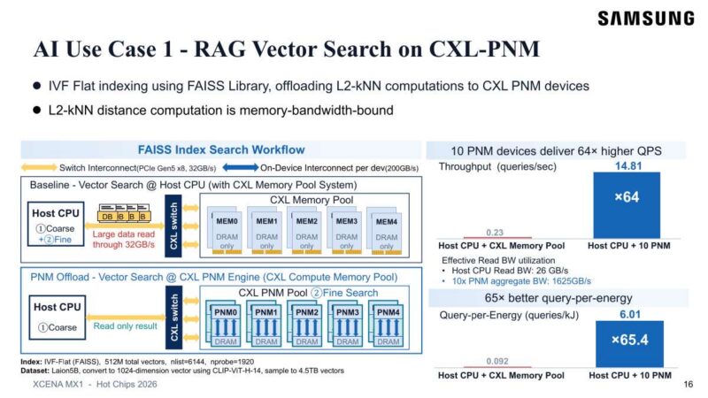 图15|Slide 16: AI Use Case 1 - RAG Vector Search on CXL-PNM
This second use case is LLM decoding with GPU-plus-PNM hybrid attention. Hybrid attention keeps hit pages on the GPU and pushes miss pages to the PNM device, which returns only the computed attention result instead of shipping the KV pages back. Here, the decode timeline compares GPU-only attention, which loads the KV cache from CXL, with the hybrid path that offloads the missed-attention work.
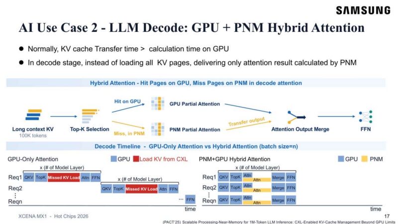 图16|Slide 17: AI Use Case 2 - LLM Decode: GPU + PNM Hybrid Attention
Samsung’s results on the hybrid decode path are the headline numbers. At 100K context, the PNM pool raises throughput by 3.35x and token-per-energy by 3.84x, shown as 17.7 versus 5.50 tokens per second and 4.31 versus 1.12 tokens per kilojoule. For this run, Samsung used LLaMA-3.1-70B INT8 across two servers, each with five MX1 devices and NVIDIA RTX Pro 6000 Blackwell GPUs.
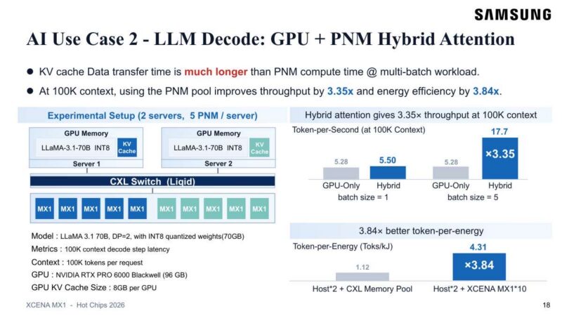 图17|Slide 18: AI Use Case 2 - LLM Decode: GPU + PNM Hybrid Attention
Taken together, XCENA and Samsung are positioning MX1 as real silicon at the heart of the computational memory wave, pairing the device, its PXL runtime, and Infinite Memory with a rack-scale Samsung pooling story.
Final Words
XCENA’s session makes a concrete case that the bottleneck for AI and analytics is memory, and that the fix can reside in a CXL device rather than in a larger host processor or a faster GPU. This combination of near-memory RISC-V compute, SSD-backed byte-addressable memory, and Samsung’s rack-scale pooling points to a memory tier that scales capacity and compute together. It will be interesting to see how this works, but I also think that SSD tiering is really interesting.
第二部分:解析(深度解读)
核心论点摘要
XCENA 与三星在 Hot Chips 2026 上联合给出的核心判断是:AI 与数据分析的瓶颈先卡在内存容量、带宽与功耗,而不是原始算力。MX1 是一颗 Type 3 CXL 器件,把三件事熔进同一个封装:
- CXL 内存扩展:4 条 DDR5-8400 通道,最大 2TB;
- SSD 级字节寻址内存(Infinite Memory):SSD 以 CXL 内存形态整体暴露给主机;
- 近内存计算:3072 个定制 RISC-V 核(MU)在内存旁做计算。
三星则把这套器件延伸到机架级 CXL 内存池,并用 Near-Data Computing(NDC)做 RAG 向量检索与 LLM decode 的混合注意力加速。
关键概念解读
- 为什么是 3072 个简单顺序 RISC-V 核,而不是少量大核? 目标负载是带宽受限、功耗敏感型的;小核让 XCENA 能在单 die 上塞下 3072 个核并把「每字节能耗」压低。开放 ISA 带来成熟工具链,且便于为内存内分析、RAG 检索、内存压缩加入自定义指令。
- 单一共享虚拟地址空间:主机与 MU 看到同一组指针,pointer-rich 结构可安全穿越,既有 malloc 代码几乎零改动即可迁到 CXL 内存;CXL-aware 分配器用每租户页表隔离不同应用的内核。
- PXL 运行时(MapReduce 风格):用 C/C++/Rust 写内核,作业分配一个或多个 subsystem,map API 把工作切到各 MU 核,分配与同步自动处理。
- Infinite Memory 的 KV Cache 故事:pinned 前缀常驻时 TTFT 仅 1.13× DRAM;靠 lookahead 预取利用器件空闲可逼近 DRAM 常驻性能(实测 Llama-3.1-8B + vLLM + LMCache + RTX 6000 Pro)。
性能数字( Intel Xeon 6767P 参考,不含空闲功耗)
| 对比基准 | 吞吐提升 | 功耗 | 能效提升 |
|---|---|---|---|
| vs host-over-CXL | 最高 4.7× | 约 1/4 | 最高 18.7× |
| vs 本地 DRAM | 2× | 约 1/4 | 6.2× |
三星 PNM 用例:10 个 PNM 设备做 RAG 向量检索(IVF Flat / FAISS,L2 kNN 卸载,512M 向量 Laion 5B 索引)相对「主机 CPU + CXL 内存池」达 64× QPS、65× 每焦耳查询数;GPU+PNM 混合注意力的 LLM decode 在 100K 上下文下吞吐 3.35×、每焦耳 token 3.84×(17.7 vs 5.50 tok/s,4.31 vs 1.12 tok/kJ,LLaMA-3.1-70B INT8,2 台服务器各 5 颗 MX1 + RTX Pro 6000 Blackwell)。
技术趋势判断
这是「计算存储/计算内存」路线在 Hot Chips 2026 的集中亮相,与本届 AMD MI400、NVIDIA Rubin 的叙事同根同源——瓶颈正从算力转向内存。CXL 作为内存织物(fabric),配合近内存计算,是三星等内存厂商把 DRAM 带宽「变现」的自然延伸。机架级参考设计(Liqid CXL switch + Blackwell GPU,20TB @ 2.7TB/s)显示 CXL 内存池正在向可落地系统演进。
投资映射:CXL 交换机(Astera Labs、Liqid 等)、内存原厂(Samsung / SK hynix)、RISC-V IP(SiFive 等)是这条路线的确定性受益环节;风险在于 CXL 生态与软件成熟度、以及「主机-over-CXL」基线的真实部署占比。
风险提示
文中倍数为厂商基准(Intel Xeon 6767P 参考,排除空闲功耗),实际收益取决于工作负载是否真正带宽受限;CXL 内存池的端到端延迟与多租户隔离未经第三方大规模验证;SSD 级内存分层的耐用性与掉电一致性需实测。本文不构成投资建议。